FPGA Tutorial: A Beginner's Guide to Programmable Logic Design in 2025
FPGAs represent one of the most versatile and powerful tools in modern digital design, allowing engineers to implement virtually any digital circuit in reconfigurable hardware. According to recent industry reports, the global FPGA market is projected to reach $13.2 billion by 2026, growing at a CAGR of 8.5% from 2021, highlighting the increasing importance of this technology across various sectors.
In this comprehensive tutorial, we'll demystify FPGAs for beginners, walking you through everything from basic concepts to your first working project. Whether you're an electronics enthusiast, a computer engineering student, or a professional looking to expand your skill set, this guide will help you navigate the exciting world of programmable logic.
FPGA Basics: What Is an FPGA and Why Should You Learn It?
Definition and Core Concepts
An FPGA (Field-Programmable Gate Array) is an integrated circuit designed to be configured by a customer or designer after manufacturing—hence the term "field-programmable." Unlike microprocessors that execute software instructions sequentially, FPGAs implement logic functions using configurable hardware blocks that operate in parallel.
Pro Tip: Think of an FPGA as a blank canvas of digital logic that you can program to become almost any digital circuit you can imagine. Unlike a microcontroller that runs ce, an FPGA becomes the hardware you design.
The key difference between FPGAs and other computing devices lies in their architecture:
Microcontrollers/CPUs: Execute instructions sequentially, even when multithreaded
ASICs: Custom-designed circuits that cannot be modified after manufacturing
FPGAs: Reconfigurable hardware that can implement custom digital circuits with true parallelism
Why Learn FPGA Design?
Learning FPGA design offers numerous benefits that make it worth the initial learning curve:
Hardware Acceleration: FPGAs can perform certain operations orders of magnitude faster than CPUs by leveraging massive parallelism
Versatility: The same FPGA can be reprogrammed for entirely different applications
Low Latency: Direct hardware implementation enables deterministic, real-time processing
Career Opportunities: According to a LinkedIn job analysis, FPGA skills command premium salaries in the job market
Cross-Disciplinary Skills: Learning FPGAs strengthens understanding of digital logic, computer architecture, and hardware/software interfaces
As one industry veteran put it:
"Learning FPGA design changes how you think about computing forever. Once you understand how to design at the hardware level, you see opportunities for optimization that software engineers often miss."
Real-World FPGA Applications
FPGAs have found their way into numerous cutting-edge applications:
Data Centers: Custom accelerators for AI/ML workloads and networking
Telecommunications: Software-defined radio and 5G infrastructure
Aerospace and Defense: Radar systems and secure communications
Automotive: Advanced driver assistance systems (ADAS)
Finance: High-frequency trading platforms requiring nanosecond precision
Consumer Electronics: Video processing in high-end displays
This video provides an excellent visual overview of FPGA applications:
FPGA Architecture: Understanding the Building Blocks
Logic Elements and Configurable Logic Blocks (CLBs)
At the heart of every FPGA are its Configurable Logic Blocks (CLBs), sometimes called Logic Elements (LEs) or Logic Cells (LCs). These are the fundamental building blocks that implement the digital logic functions you design.
Each CLB typically contains:
Look-Up Tables (LUTs): Small memory elements that can implement any logical function with a limited number of inputs (typically 4-6)
Flip-Flops: Storage elements that hold state information
Multiplexers: Allow selection between different signals
Carry Logic: Specialized circuitry for efficient arithmetic operations
Interconnect Structure
The programmable interconnect is what makes FPGAs truly flexible. This network of routing resources:
Connects CLBs to each other
Links CLBs to specialized blocks and I/O pins
Can be configured to create any desired signal path
Modern FPGAs employ hierarchical routing structures to balance flexibility with performance:
Local Interconnect: Connects adjacent CLBs with minimal delay
Regional Interconnect: Spans larger distances across the chip
Global Interconnect: Distributes clock and other critical signals with controlled skew
Specialized Blocks
Beyond the basic logic fabric, modern FPGAs include specialized hardware blocks:
Block RAM (BRAM): Dedicated memory blocks for storing data
Digital Signal Processing (DSP) Slices: Optimized for multiply-accumulate operations
Clock Management Tiles: PLLs and DCMs for clock synthesis and distribution
High-Speed Transceivers: For SerDes and other high-speed I/O
Hard Processors: Some FPGAs include embedded ARM or RISC-V cores
FPGA Resource | Function | Advantage | Common Uses |
Look-Up Tables (LUTs) | Implement combinatorial logic | Flexibility to create any logic function | State machines, decoders, arithmetic |
Block RAM | On-chip memory | High-bandwidth, low-latency storage | FIFOs, buffers, lookup tables |
DSP Slices | Math operations | High-performance multiply-accumulate | Signal processing, ML acceleration |
PLLs/DCMs | Clock management | Precise timing control | Clock multiplication, phase shifting |
I/O Blocks | Interface with external devices | Support for multiple I/O standards | Memory interfaces, peripheral connections |
FPGA Families and Vendors
The major FPGA vendors each offer different product families optimized for various applications:
Xilinx (AMD): Artix, Kintex, Virtex, Spartan, and Versal series
Intel (formerly Altera): Cyclone, Arria, and Stratix series
Lattice Semiconductor: iCE40, ECP, and Nexus series
Microchip (formerly Microsemi): PolarFire and IGLOO series
Each family targets different performance, power, and cost points. For beginners, the entry-level families (Xilinx Artix/Spartan, Intel Cyclone, Lattice iCE40) offer the best balance of capability and affordability.
FPGA Development Flow: From Design to Implementation
Overview of the Design Flow
The FPGA development process follows a structured flow from concept to working hardware:
Design Entry: Creating your design using HDL or schematic tools
Functional Simulation: Verifying logical correctness
Synthesis: Converting HDL to a netlist of FPGA primitives
Implementation: Placing and routing the design on the FPGA fabric
Timing Analysis: Ensuring the design meets timing requirements
Bitstream Generation: Creating the configuration file
Programming: Loading the bitstream onto the FPGA
Hardware Verification: Testing the design in the actual hardware
Design Entry Methods
You have several options for creating your FPGA design:
Hardware Description Languages (HDLs)
The most common approach is coding in an HDL:
Verilog: C-like syntax, popular in industry and academia
VHDL: Ada-inspired, strongly typed language with verbose syntax
SystemVerilog: Extended Verilog with verification features
// Simple Verilog example: A 2-to-1 multiplexer
module mux_2to1 (
input wire sel,
input wire a,
input wire b,
output wire out
);
assign out = sel ? b : a;
endmodule
High-Level Synthesis (HLS)
For higher productivity, especially for algorithm-intensive designs:
C/C++ based: Xilinx Vitis HLS, Intel HLS Compiler
OpenCL: For parallel computing applications
Domain-specific languages: Like Chisel (Scala-based HDL)
Block Diagram and IP Integration
Most vendor tools also support graphical design methods:
Block diagrams: Connecting pre-built IP cores visually
Schematic entry: Drawing the circuit using graphical symbols
Simulation
Simulation is crucial at multiple stages of the design flow:
Behavioral simulation: Tests the functional correctness of your HDL code
Post-synthesis simulation: Verifies the logic after synthesis
Timing simulation: Accounts for actual delays in the implemented design
Popular simulators include:
Vendor tools: Xilinx Vivado Simulator, Intel ModelSim-Intel FPGA Edition
Third-party: ModelSim/QuestaSim, Aldec Active-HDL, Verilator (open-source)
Important Note: Never skip simulation! While it may be tempting to go straight to hardware testing, simulation can catch many bugs earlier in the development process, saving significant debugging time.
Synthesis and Implementation
Once your design simulates correctly, the next steps involve:
Synthesis: Converting HDL to optimized gate-level representation
Technology mapping: Mapping generic gates to FPGA-specific resources
Placement: Determining the physical location of logic elements on the chip
Routing: Connecting the placed elements using the FPGA's routing resources
Timing analysis: Ensuring signals meet setup and hold time requirements
Modern FPGA tools automate much of this process but often require designer guidance through constraints.
Constraints and Timing Closure
Design constraints provide essential guidance to the implementation tools:
Timing constraints: Specify clock frequencies and relationships
Pin assignments: Map logical signals to physical FPGA pins
Area constraints: Control placement for critical components
Power constraints: Guide tools to optimize for power consumption
Here's a simple example of an XDC timing constraint for Xilinx FPGAs:
# Define a 100 MHz clock
create_clock -period 10.000 -name sys_clk -waveform {0.000 5.000} [get_ports clk]
FPGA Programming
The final step is programming the FPGA with your design:
Volatile programming: Configuration is lost when power is removed (SRAM-based FPGAs)
Non-volatile programming: Configuration persists through power cycles (Flash-based FPGAs)
Programming methods: JTAG, SPI, USB, SD card, etc.
Most development boards provide multiple programming options for convenience.
For a visual walkthrough of the development flow, watch this helpful tutorial:
HDL Programming: Verilog and VHDL Fundamentals
Choosing Between Verilog and VHDL
One of the first decisions you'll face is which Hardware Description Language (HDL) to use. Both Verilog and VHDL are industry standards with robust support.
Verilog Advantages:
More concise, C-like syntax
Slightly easier learning curve for programmers
Popular in ASIC design and certain industries (especially in the US and Asia)
VHDL Advantages:
Strongly typed with extensive checking
Better for large, team-based projects
Popular in defense, aerospace, and European industries
Many engineers learn both languages eventually, but I recommend starting with Verilog for beginners due to its simpler syntax. This tutorial will use Verilog for examples.
HDL vs. Traditional Programming Languages
HDLs differ fundamentally from software programming languages:
Parallelism: In HDLs, operations described in different blocks can execute simultaneously
Hardware inference: Code describes actual hardware structures, not sequential instructions
Time concept: HDLs have built-in timing concepts (clocks, delays)
Signal vs. variable: Signals represent physical wires with electrical properties
Consider this Verilog example:
// These two assignments happen simultaneously, not sequentially
assign a = b + c;
assign x = y * z;
In software, these would execute in sequence. In HDL, they represent separate hardware that operates in parallel.
Essential Verilog Concepts
Module Structure
Every Verilog design centers around modules - the building blocks of your design:
module counter_example(
input wire clk,
input wire reset,
output reg [7:0] count
);
// Module implementation goes here
endmodule
Data Types and Signals
Verilog has several important data types:
wire: Represents physical connections between components (combinational)
reg: Can store values (used for sequential logic)
integer, real: General-purpose variables for test benches and calculations
parameter: Constants used for customization
wire [7:0] data_bus; // 8-bit wire (combinational)
reg [15:0] register_value; // 16-bit register (sequential)
parameter COUNTER_WIDTH = 8; // Constant parameter
Operators
Verilog provides a rich set of operators similar to C:
Arithmetic: +, -, *, /, %
Logical: &&, ||, !
Bitwise: &, |, ^, ~
Relational: ==, !=, <, >, <=, >=
Reduction: &a (AND all bits of a), |b (OR all bits of b)
Shift: <<, >>
Procedural Blocks
Verilog uses procedural blocks to describe sequential behavior:
always @(posedge clk): Triggered on rising clock edge (sequential logic)
always @(*): Triggered whenever any input changes (combinational logic)
initial: Executes once at the beginning (for simulation only)
Here's a simple counter example using an always block:
// 8-bit counter with synchronous reset
always @(posedge clk) begin
if (reset)
count <= 8'b0; // Reset to zero
else
count <= count + 1; // Increment
end
Behavioral vs. Structural Modeling
Verilog supports multiple modeling styles:
Behavioral: Describes what the circuit does (functionality)
Structural: Describes how the circuit is built (connections)
Dataflow: Uses continuous assignments (assign statements)
Most designs use a mix of these styles for different parts of the circuit.
Common HDL Patterns and Best Practices
Synchronous Design
Most FPGA designs follow synchronous design principles, where all state changes occur on clock edges:
// Good synchronous design pattern
always @(posedge clk) begin
if (reset)
state <= IDLE;
else
state <= next_state;
end
State Machines
Finite State Machines (FSMs) are a common FPGA design pattern, typically implemented using a two-process model:
// State register (sequential logic)
always @(posedge clk) begin
if (reset)
current_state <= IDLE;
else
current_state <= next_state;
end// Next state logic (combinational)
always @(*) begin
case (current_state)
IDLE: next_state = data_valid ? READ : IDLE;
READ: next_state = data_end ? IDLE : PROCESS;
PROCESS: next_state = WRITE;
WRITE: next_state = IDLE;
default: next_state = IDLE;
endcase
end
Avoiding Common Mistakes
Here are some common HDL pitfalls to avoid:
Latches: Incomplete conditional statements can create unintended latches
Combinational loops: Feedback paths without registers cause instability
Multiple drivers: Multiple sources driving the same signal
Race conditions: Dependent sequential logic that relies on evaluation order
For more on Verilog programming, you can explore these resources from UTMEL's integrated circuits blog, which offers practical examples and tips.
FPGA Development Boards for Beginners
What to Look for in Your First FPGA Board
Choosing the right development board is crucial for a positive learning experience. Consider these factors:
FPGA Size and Family: Newer families offer better tools and features, but older ones may have more community support
Onboard Peripherals: LEDs, switches, displays, and connectors provide immediate feedback
Programming Interface: USB programming is most convenient for beginners
Documentation and Tutorials: Good documentation accelerates learning
Community Support: Active forums help solve inevitable issues
Price Point: Balance features with budget (typically $50-300 for beginner boards)
Recommended Beginner-Friendly Boards
Here are some excellent starter FPGA boards with their key features:
| Board | FPGA Model | Key Features | Price | Best For |
|---|---|---|---|---|
| Xilinx (AMD) | ||||
| Digilent Basys 3 | Artix-7 | • USB programming• Plenty of switches, LEDs, 7-segment displays• Excellent documentation | ~$149 | Students and beginners |
| Digilent Arty A7 | Artix-7 | • More I/O options than Basys 3• Arduino-compatible headers• Good for embedded systems | ~$129-$249<br>(depending on FPGA size) | Embedded systems developers |
| Intel (Altera) | ||||
| Terasic DE10-Lite | MAX 10 | • Built-in ADC• Many switches and LEDs• Accelerometer and VGA output | ~$130 | University education |
| Terasic DE0-Nano | Cyclone IV | • Small form factor• Accelerometer and ADC<br>• GPIO expansion | ~$90 | Budget-conscious developers |
| Lattice | ||||
| iCEBreaker | iCE40 | • Open-source toolchain support• PMOD connectors for expansion• Very affordable | ~$69 | Open-source enthusiasts |
| TinyFPGA BX | iCE40 | • Tiny USB stick forma | ~$38 | Minimal, space-constrained projects |
Frequently Asked Questions About FPGAs
General FPGA Questions
What's the difference between an FPGA and a microcontroller?
An FPGA is a reconfigurable hardware device that performs operations in parallel through custom digital circuits you design. A microcontroller is a fixed-architecture device that executes software instructions sequentially. FPGAs offer higher performance for parallel tasks but typically require more power and are more complex to program.
How long does it take to learn FPGA design?
The basic concepts can be learned in a few weeks, but becoming proficient typically takes 3-6 months of regular practice. Mastering advanced FPGA design can take years, similar to other specialized engineering fields. The learning curve depends on your background in digital logic, programming experience, and the complexity of projects you tackle.
Can FPGAs replace CPUs or GPUs?
FPGAs excel at specific types of workloads, particularly those requiring custom datapaths, precise timing, or highly parallel operations. They generally don't replace CPUs for general-purpose computing but often complement them as accelerators. For certain machine learning and data processing tasks, FPGAs can outperform both CPUs and GPUs in performance-per-watt, but they require specialized design skills to program effectively.
Technical Questions
What size FPGA do I need for my project?
Consider these factors:
Logic resources: Estimate your design's flip-flop and LUT requirements
Memory needs: Calculate required Block RAM for buffers and storage
Clock frequency: Higher frequencies may require higher-grade FPGAs
I/O requirements: Count the number and types of I/O pins needed
Special resources: DSP blocks, transceivers, hard processors
Add a 30-50% margin to your estimates for future expansion and unexpected requirements.
How do I choose between Verilog and VHDL?
Both languages are capable of designing any digital circuit. Consider:
Your background (C/Java programmers often prefer Verilog)
Industry standards in your region (Europe often uses VHDL, US/Asia often uses Verilog)
Available examples and IP for your project
Team preferences for collaborative projects
Many engineers learn both languages eventually, as existing projects may use either one.
What causes timing failures in FPGA designs?
Timing failures occur when signals cannot propagate through combinational logic within the clock period. Common causes include:
Excessive logic between registers (long paths)
High fan-out signals driving many destinations
Poor placement with related logic spread across the chip
Clock domain crossing issues
Inadequate constraints or unrealistic clock frequencies
Practical Questions
How much does FPGA development cost?
For beginners:
Development board: $50-300
Software tools: Often free for smaller FPGAs
Learning resources: Many free tutorials and books from $30-100
For professional development:
Professional FPGA boards: $500-5,000+
Full-featured software licenses: $2,000-5,000/year
IP cores: From free to tens of thousands per core
Development time: The largest cost is typically engineering time
Can I use open-source tools for FPGA development?
Yes, open-source FPGA tools have advanced significantly:
Yosys + nextpnr: Support for Lattice and limited Xilinx devices
Project IceStorm: Full flow for Lattice iCE40 FPGAs
Project X-Ray/SymbiFlow: Growing support for Xilinx FPGAs
LiteX: SoC builder with various CPU and peripheral options
These tools work best on Linux and currently support a subset of commercial FPGAs, but the ecosystem is growing rapidly.
What industries use FPGAs the most?
FPGAs are widely used in:
Telecommunications: Wireless base stations, networking equipment
Aerospace and Defense: Radar, secure communications, avionics
Data Centers: Accelerated computing, custom networking
Automotive: Advanced driver assistance systems (ADAS)
Industrial: Motion control, real-time monitoring
Medical: Imaging equipment, diagnostic devices
Consumer Electronics: High-end cameras, displays, audio equipment
The demand for FPGA engineers continues to grow across these sectors.
Quick Checklist for FPGA Beginners
Use this checklist to ensure you're on the right track:
Understand basic digital logic (gates, flip-flops, multiplexers)
Learn at least one HDL (Verilog or VHDL) at a basic level
Set up a development environment for your chosen FPGA
Complete a simple LED blinking project
Practice simulation before implementing designs
Join an FPGA community or forum for support
Create increasingly complex projects to build skills
Document your designs for future reference
For answers to more specific questions about FPGA components and applications, visit UTMEL's comprehensive FPGA FAQs.
Conclusion
FPGAs represent a fascinating middle ground between software and hardware, offering incredible flexibility and performance for those willing to master their unique development flow. From the building blocks of configurable logic to the sophisticated tools used to design and debug complex systems, we've covered the essential knowledge you need to begin your FPGA journey.
As you progress from simple projects to more advanced applications, remember that FPGA design is both an art and a science. The ability to think in terms of parallel hardware execution rather than sequential software steps is a valuable skill that will change how you approach problem-solving in digital systems.
Whether you're interested in high-performance computing, embedded systems, signal processing, or any other field where customized digital hardware provides an advantage, FPGAs offer a powerful and accessible platform for innovation. With the growing availability of affordable development boards and improved design tools, there's never been a better time to add FPGA skills to your engineering toolkit.
What's Next?
To continue your FPGA learning journey:
Complete several small projects to build confidence
Join FPGA forums and communities to learn from others
Explore vendor tutorials and reference designs
Consider specialized applications matching your interests
Experiment with more advanced techniques as your skills grow
For a comprehensive collection of FPGA components, development boards, and educational resources, visit UTMEL.com, where you'll find everything you need for your FPGA projects, from beginner to advanced.
Last Updated: April 15th, 2025
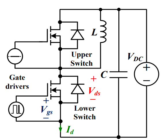 Discovering New and Advanced Methodology for Determining the Dynamic Characterization of Wide Bandgap DevicesSaumitra Jagdale15 March 20242448
For a long era, silicon has stood out as the primary material for fabricating electronic devices due to its affordability, moderate efficiency, and performance capabilities. Despite its widespread use, silicon faces several limitations that render it unsuitable for applications involving high power and elevated temperatures. As technological advancements continue and the industry demands enhanced efficiency from devices, these limitations become increasingly vivid. In the quest for electronic devices that are more potent, efficient, and compact, wide bandgap materials are emerging as a dominant player. Their superiority over silicon in crucial aspects such as efficiency, higher junction temperatures, power density, thinner drift regions, and faster switching speeds positions them as the preferred materials for the future of power electronics.
Read More A Comprehensive Guide to FPGA Development BoardsUTMEL11 September 202513842
This comprehensive guide will take you on a journey through the fascinating world of FPGA development boards. We’ll explore what they are, how they differ from microcontrollers, and most importantly, how to choose the perfect board for your needs. Whether you’re a seasoned engineer or a curious hobbyist, prepare to unlock new possibilities in hardware design and accelerate your projects. We’ll cover everything from budget-friendly options to specialized boards for image processing, delve into popular learning paths, and even provide insights into essential software like Vivado. By the end of this article, you’ll have a clear roadmap to navigate the FPGA landscape and make informed decisions for your next groundbreaking endeavor.
Read More Applications of FPGAs in Artificial Intelligence: A Comprehensive GuideUTMEL29 August 20253426
This comprehensive guide explores FPGAs as powerful AI accelerators that offer distinct advantages over traditional GPUs and CPUs. FPGAs provide reconfigurable hardware that can be customized for specific AI workloads, delivering superior energy efficiency, ultra-low latency, and deterministic performance—particularly valuable for edge AI applications. While GPUs excel at parallel processing for training, FPGAs shine in inference tasks through their adaptability and power optimization. The document covers practical implementation challenges, including development complexity and resource constraints, while highlighting solutions like High-Level Synthesis tools and vendor-specific AI development suites from Intel and AMD/Xilinx. Real-world applications span telecommunications, healthcare, autonomous vehicles, and financial services, demonstrating FPGAs' versatility in mission-critical systems requiring real-time processing and minimal power consumption.
Read More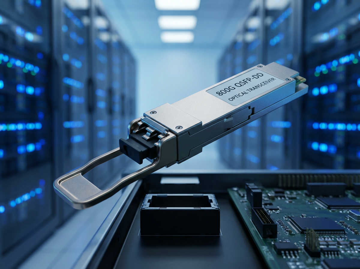 800G Optical Transceivers: The Guide for AI Data CentersUTMEL24 December 20253388
The complete guide to 800G Optical Transceiver standards (QSFP-DD vs. OSFP). Overcome supply shortages and scale your AI data center with Utmel Electronic.
Read More Xilinx FPGAs: From Getting Started to Advanced Application DevelopmentUTMEL09 September 20254172
This guide is your comprehensive roadmap to understanding and mastering the world of Xilinx FPGA technology. From selecting your first board to deploying advanced AI applications, we'll cover everything you need to know to unlock the potential of these remarkable devices. The global FPGA market is on a significant growth trajectory, expected to expand from USD 8.37 billion in 2025 to USD 17.53 billion by 2035. This surge is fueled by the relentless demand for high-performance, adaptable computing in everything from 5G networks and data centers to autonomous vehicles and the Internet of Things (IoT). This guide will walk you through the key concepts, tools, and products in the Xilinx ecosystem, ensuring you're well-equipped to be a part of this technological revolution.
Read More
Subscribe to Utmel !
![FM31L276-GTR]() FM31L276-GTR
FM31L276-GTRCypress Semiconductor Corp
![TLP5832(D4,E]() TLP5832(D4,E
TLP5832(D4,EToshiba Semiconductor and Storage
![ATSHA204A-XHCZ-T]() ATSHA204A-XHCZ-T
ATSHA204A-XHCZ-TMicrochip Technology
![AT88SC0104CA-MJTG]() AT88SC0104CA-MJTG
AT88SC0104CA-MJTGMicrochip Technology
![APT1211S]() APT1211S
APT1211SPanasonic Electric Works
![FOD410SDV]() FOD410SDV
FOD410SDVON Semiconductor
![FLC21-135A]() FLC21-135A
FLC21-135ASTMicroelectronics
![CS8190EDWF20G]() CS8190EDWF20G
CS8190EDWF20GON Semiconductor
![TLP5752(D4-LF4,E]() TLP5752(D4-LF4,E
TLP5752(D4-LF4,EToshiba Semiconductor and Storage
![TLP5751(D4-LF4,E]() TLP5751(D4-LF4,E
TLP5751(D4-LF4,EToshiba Semiconductor and Storage


 Product
 Brand
Brand Articles
 Tools
Tools


