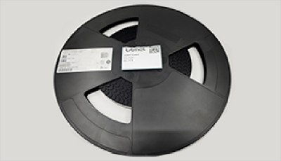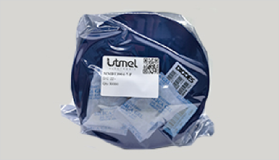

Taiwan Semiconductor TSM085NB03DCR
Manufacturer No:
TSM085NB03DCR
Tiny WHSLManufacturer:
Utmel No:
2436-TSM085NB03DCR
Package:
-
Description:
30V 51A Dual N-Channel Power MOSFET
Quantity:
Unit Price: $1.158008
Ext Price: $1.16
Delivery:


Payment:


In Stock : 36
Minimum: 1 Multiples: 1
Qty
Unit Price
Ext Price
1
$1.158008
$1.16
10
$1.092461
$10.92
100
$1.030623
$103.06
500
$0.972286
$486.14
1000
$0.917251
$917.25
Want a lower wholesale price? Please send RFQ, we will respond immediately.
RFQ Now
Add to RFQ list
You may place an order without registering to Utmel.
We strongly suggest you sign in before purchasing as you can track your order in real time.
For your convenience, we accept multiple payment methods in USD, including PayPal, Credit Card, and wire transfer.
RFQ (Request for Quotations)It is recommended to request for quotations to get the latest prices and inventories about the part.
Our sales will reply to your request by email within 24 hours.
1. You'll receive an order information email in your inbox. (Please remember to check the spam folder if you didn't hear from us).
2. Since inventories and prices may fluctuate to some extent, the sales manager is going to reconfirm the order and let you know if there are any updates.
- TypeParameter
- Lifecycle Status
Lifecycle Status refers to the current stage of an electronic component in its product life cycle, indicating whether it is active, obsolete, or transitioning between these states. An active status means the component is in production and available for purchase. An obsolete status indicates that the component is no longer being manufactured or supported, and manufacturers typically provide a limited time frame for support. Understanding the lifecycle status is crucial for design engineers to ensure continuity and reliability in their projects.
Production (Last Updated: 3 years ago) - Breakdown Voltage / V51 V
- Manufacturer Lifecycle StatusACTIVE (Last Updated: 3 years ago)
- Reverse Stand-off Voltage24 V
- Number of Channels2
- Power Dissipation
the process by which an electronic or electrical device produces heat (energy loss or waste) as an undesirable derivative of its primary action.
200 mW - Max Reverse Leakage Current
Max Reverse Leakage Current refers to the maximum amount of current that can flow through a semiconductor device, such as a diode or transistor, when it is reverse biased. This current is an important parameter as it indicates the level of unintended current that can flow when the device is not conducting in the forward direction. High values of reverse leakage current can lead to power loss, reduced efficiency, and may affect the performance and reliability of electronic circuits. It is particularly critical in applications where precise current control and low power consumption are necessary.
1 µA - Clamping Voltage
Clamping voltage is a term used in electronic components, particularly in devices like diodes and transient voltage suppressors. It refers to the maximum voltage level at which the component can effectively limit or clamp the voltage across its terminals. When the voltage across the component exceeds the clamping voltage, the component conducts and effectively limits the voltage to that level, protecting the circuit from overvoltage conditions. Clamping voltage is an important parameter to consider when selecting components for applications where voltage spikes or surges may occur, as it determines the level at which the component will start to protect the circuit.
70.1 V - Peak Pulse Current
The peak pulse power rating of a TVS diode is defined as the instantaneous power dissipated by a device for a given pulse condition, and is a measure of the power that is dissipated in the TVS junction during a given transient event.
21.4 A - Peak Pulse Power
Peak Pulse Power is a parameter used to specify the maximum amount of power that an electronic component can handle during a transient event, such as a surge or spike in voltage or current. It indicates the maximum power dissipation capability of the component for a short duration. This parameter is important for protecting electronic circuits from damage caused by sudden high-energy events. Peak Pulse Power is typically expressed in watts and is crucial for selecting components that can withstand transient overloads without failing. It helps ensure the reliability and longevity of electronic systems in various applications.
1.5 kW - Test Current
Test Current refers to a specified amount of electrical current applied to an electronic component during testing to evaluate its performance and characteristics. This current is typically defined by manufacturers to ensure that the component operates within its designed parameters. By measuring how the component reacts to this test current, engineers can determine its reliability, efficiency, and suitability for specific applications.
2.5 mA - Drain to Source Voltage (Vdss)
The Drain to Source Voltage (Vdss) is a key parameter in electronic components, particularly in field-effect transistors (FETs) such as MOSFETs. It refers to the maximum voltage that can be applied between the drain and source terminals of the FET without causing damage to the component. Exceeding this voltage limit can lead to breakdown and potentially permanent damage to the device.Vdss is an important specification to consider when designing or selecting components for a circuit, as it determines the operating range and reliability of the FET. It is crucial to ensure that the Vdss rating of the component is higher than the maximum voltage expected in the circuit to prevent failures and ensure proper functionality.In summary, the Drain to Source Voltage (Vdss) is a critical parameter that defines the maximum voltage tolerance of a FET component and plays a significant role in determining the overall performance and reliability of electronic circuits.
30 V - Forward Voltage
the amount of voltage needed to get current to flow across a diode.
1 V - Zener Voltage
The Zener voltage is a crucial parameter in Zener diodes, which are specialized semiconductor devices designed to maintain a constant voltage across their terminals when operated in the reverse-biased mode. The Zener voltage, also known as the breakdown voltage, is the voltage at which the Zener diode starts conducting in the reverse direction. This voltage is carefully controlled during the manufacturing process and is a key characteristic that determines the diode's functionality in voltage regulation and protection circuits. Zener diodes are commonly used in various electronic applications to stabilize voltage levels and protect sensitive components from voltage spikes.
75 V - Reverse Recovery Time
Reverse Recovery Time is a key parameter in semiconductor devices, particularly diodes and transistors. It refers to the time taken for a diode or transistor to switch from conducting in the forward direction to blocking in the reverse direction when the polarity of the voltage across the device is reversed. This parameter is crucial in applications where fast switching speeds are required, as a shorter reverse recovery time allows for quicker response times and improved efficiency. Reverse Recovery Time is typically specified in datasheets for electronic components and is an important consideration in circuit design to ensure optimal performance and reliability.
50 ns - Max Repetitive Reverse Voltage (Vrrm)
The Max Repetitive Reverse Voltage (Vrrm) is a crucial parameter in electronic components, particularly in diodes and transistors. It refers to the maximum voltage that can be applied across the component in the reverse direction without causing damage. This parameter is important for ensuring the proper functioning and longevity of the component in circuits where reverse voltage may be present. Exceeding the Vrrm rating can lead to breakdown and failure of the component, so it is essential to carefully consider this specification when designing or selecting components for a circuit.
250 V - Gate to Source Voltage (Vgs)
The Gate to Source Voltage (Vgs) is a crucial parameter in electronic components, particularly in field-effect transistors (FETs) such as MOSFETs. It refers to the voltage difference between the gate and source terminals of the FET. This voltage determines the conductivity of the FET and controls the flow of current through the device. By varying the Vgs, the FET can be switched on or off, allowing for precise control of electronic circuits. Understanding and properly managing the Vgs is essential for ensuring the reliable and efficient operation of FET-based circuits.
1.8 V - Input Capacitance
The capacitance between the input terminals of an op amp with either input grounded. It is expressed in units of farads.
1.091 nF - Max Breakdown Voltage
The "Max Breakdown Voltage" of an electronic component refers to the maximum voltage that the component can withstand across its terminals before it breaks down and allows current to flow uncontrollably. This parameter is crucial in determining the operating limits and safety margins of the component in a circuit. Exceeding the maximum breakdown voltage can lead to permanent damage or failure of the component. It is typically specified by the manufacturer in datasheets to guide engineers and designers in selecting the appropriate components for their applications.
9.8 V - Max Forward Surge Current (Ifsm)
Max Forward Surge Current (Ifsm) is a parameter used to specify the maximum peak current that a diode or other electronic component can withstand for a short duration during a surge event. Surge currents can occur due to sudden changes in voltage or power supply fluctuations, and the Ifsm rating helps determine the component's ability to handle such transient overloads without being damaged. It is important to consider the Ifsm rating when selecting components for applications where surge currents are expected, such as in power supplies, motor drives, and other high-power circuits. Exceeding the Ifsm rating can lead to overheating, degradation, or failure of the component, so it is crucial to ensure that the chosen component can safely handle the expected surge currents in the circuit.
2.5 A - Max Junction Temperature (Tj)
Max Junction Temperature (Tj) refers to the maximum allowable temperature at the junction of a semiconductor device, such as a transistor or integrated circuit. It is a critical parameter that influences the performance, reliability, and lifespan of the component. Exceeding this temperature can lead to thermal runaway, breakdown, or permanent damage to the device. Proper thermal management is essential to ensure the junction temperature remains within safe operating limits during device operation.
150 °C - Min Breakdown Voltage
Min Breakdown Voltage is the minimum voltage at which an electronic component, typically a diode or transistor, begins to conduct electricity in the reverse direction. When the applied voltage exceeds this threshold, the component can undergo breakdown, leading to a significant increase in reverse current. This parameter is crucial for ensuring that components operate safely within their designed voltage limits to prevent damage or malfunction.
25.4 V


