Advanced CMOS Devices with Wide Bandgap and Ultrawide Bandgap Technologies
The choice for the design based on complementary metal–oxide semiconductors arise from its numerous advantages in logic family applications. CMOS offers straightforward driving facilitated by the gate oxide, a robust fan-out capability, and high input impedance. Its benefits extend to near rail-to-rail swing due to the complementary pair structure and low static power consumption.
CMOS design offers compatibility with memory devices and high device density. Beyond digital design, complementary devices enhance various circuits, such as those employing active-load architectures or exploiting flexibility to switch on either the low side or the high side. When faced with limitations, circuit designers adapt, as seen in the adoption of direct-coupled FET logic in instances where pMOS is unavailable but both depletion-mode and enhancement nMOS devices are integrated, as observed in various Gallium Nitride processes.
It is also important to know the scope of the device based on its configuration and how it is placed. Traditionally, vertical devices have subdued the high density and power silicon market as they could have contact with both the bottom and upper layers of the epitaxial layers.
On the other hand, when achieving close integration of power devices and controls it is of utmost importance to minimize connection parasitic for high operating frequencies, therefore lateral devices emerge as the preferred choice, particularly within the control circuitry. This preference arises due to their seamless compatibility with standard integrated circuit layouts. On-chip interconnects prove to be superior in terms of performance and reliability compared to configurations involving bumps, traces, wire bonds, fusing material, and other elements that would otherwise compose a complete system from standalone parts. This on-chip integration not only enhances reliability but also boosts performance, enabling operation at higher frequencies. Consequently, it facilitates the reduction in the size of large reactive elements.
Exploring new and Improved Wide Bandgap and Ultrawide Bandgap Materials for CMOS Devices
The selection of materials in the manufacturing of CMOS devices significantly influences their performance and capabilities. Silicon has long been the foundation of CMOS devices, offering scalability and reliability, but the integration of wide bandgap materials like Silicon Carbide and Gallium Nitride has escorted in improvements in breakdown voltages and switching speeds. Lateral devices, particularly in power and control integration, present advantages in compatibility and reduced parasitic at high frequencies.
The quest for innovation and discovery of new and improved materials extends to ultrawide bandgap materials like diamond, holding promise for advanced CMOS devices with exceptional thermal conductivity. Understanding the impact of diverse materials is crucial in exploiting the dynamic landscape of CMOS manufacturing, paving the way for more efficient and high-performance electronic devices. The most suited and talked about material for CMOS devices is Silicon Carbide as it already has an established platform with extreme condition studies and complex digital circuit designs.
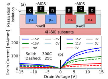
One of the most striking features of Silicon Carbide is its extensive temperature operating range, which is between 200◦C to 300◦C for high-temperature silicon-on-insulator, that is used in NASA’s JFET circuits, and it is capable of handling extremely harsh space conditions. On the other hand, SiC MOS devices are facing significantly tougher barriers like high interface trap density and low inversion-channel mobility. In order to tackle this issue, the state-of-the-art 1.2-μm HiTSiC process designed by Raytheon as shown in Figure 1 is the Industrial standard that employs two separate doped p and n wells in order to seamlessly work at 15 V.

Figure 1: Raytheon’s 1.2-μm State of the Art HiTSiC process Which Involves the Integration of Doped P and N wells
On the other hand, currently, there is no production of GaN CMOS as there is much research required in manufacturing and analysis, therefore it is vital to understand the barriers of GaN HEMTS. One of the obstacles faced by these structures relates directly to ohmic contacts. Although many research and studies do not clearly document their findings on contacts, the Schottky nature often becomes apparent in the output characteristics.
Among the most promising approaches to date, achieving contacts on the scale of a few millimeters involves heavily doped InGaN layers positioned on top of the high-density hole gases of GaN/AlN. This p-contact technique, presently incorporating less than 10% Indium, holds potential for further exploration, especially in the context of LEDs. However, distinguishing structures for contact, access, and/or gate regions remains a challenging process due to the complexities associated with ion implantation in GaN. While n-type regrowth is well-advanced for HEMT ohmic contacts, p-type regrowth faces the additional constraint of recreating or preserving the delicate hole gas, risking a reduction in local conductivity.
It is pretty evident the scale of devices is reducing with time, and materials like Silicon are becoming obsolete, therefore the need for better materials using Wide bandgap technology is of utmost importance. The choice of complementary metal–oxide semiconductors in electronic design brings forth a variety of advantages, particularly in logic family applications. The unique characteristics of CMOS, including straightforward driving, robust fan-out capability, high input impedance, near rail-to-rail swing, and low static power consumption, make it a preferred choice.
Beyond digital design, the adaptability of complementary devices enhances various circuits, showcasing their versatility. Meanwhile, the configuration and placement of devices, whether vertical or lateral, play a crucial role in optimizing performance based on specific application requirements. On-chip integration proves superior in terms of performance and reliability, paving the way for more efficient and high-performance electronic devices. Additionally, the choice of materials, with a focus on Silicon Carbide and other wide bandgap materials, continues to shape the dynamic landscape of CMOS manufacturing, providing scalability, reliability, and improved capabilities for future electronic devices.
As we delve into specific material considerations, Silicon Carbide emerges as a notable player due to its extensive temperature operating range and established platform. Despite facing challenges like high interface trap density and low inversion-channel mobility, advanced processes like the 1.2-μm HiTSiC demonstrate the ongoing efforts to overcome these obstacles. Conversely, the field of Gallium Nitride CMOS is still in the research stage, with significant hurdles in manufacturing and analysis. The discussion on GaN High Electron Mobility Transistors highlights the difficulties related to ohmic contacts, especially in the context of ion implantation challenges and the delicate balance required for p-type regrowth. The pursuit of innovative materials and manufacturing techniques remains crucial for advancing both Silicon Carbide and GaN technologies, offering the promise of more efficient and reliable electronic devices in the future.
 Discovering New and Advanced Methodology for Determining the Dynamic Characterization of Wide Bandgap DevicesSaumitra Jagdale15 March 20242498
For a long era, silicon has stood out as the primary material for fabricating electronic devices due to its affordability, moderate efficiency, and performance capabilities. Despite its widespread use, silicon faces several limitations that render it unsuitable for applications involving high power and elevated temperatures. As technological advancements continue and the industry demands enhanced efficiency from devices, these limitations become increasingly vivid. In the quest for electronic devices that are more potent, efficient, and compact, wide bandgap materials are emerging as a dominant player. Their superiority over silicon in crucial aspects such as efficiency, higher junction temperatures, power density, thinner drift regions, and faster switching speeds positions them as the preferred materials for the future of power electronics.
Read More A Comprehensive Guide to FPGA Development BoardsUTMEL11 September 202515589
This comprehensive guide will take you on a journey through the fascinating world of FPGA development boards. We’ll explore what they are, how they differ from microcontrollers, and most importantly, how to choose the perfect board for your needs. Whether you’re a seasoned engineer or a curious hobbyist, prepare to unlock new possibilities in hardware design and accelerate your projects. We’ll cover everything from budget-friendly options to specialized boards for image processing, delve into popular learning paths, and even provide insights into essential software like Vivado. By the end of this article, you’ll have a clear roadmap to navigate the FPGA landscape and make informed decisions for your next groundbreaking endeavor.
Read More Applications of FPGAs in Artificial Intelligence: A Comprehensive GuideUTMEL29 August 20253813
This comprehensive guide explores FPGAs as powerful AI accelerators that offer distinct advantages over traditional GPUs and CPUs. FPGAs provide reconfigurable hardware that can be customized for specific AI workloads, delivering superior energy efficiency, ultra-low latency, and deterministic performance—particularly valuable for edge AI applications. While GPUs excel at parallel processing for training, FPGAs shine in inference tasks through their adaptability and power optimization. The document covers practical implementation challenges, including development complexity and resource constraints, while highlighting solutions like High-Level Synthesis tools and vendor-specific AI development suites from Intel and AMD/Xilinx. Real-world applications span telecommunications, healthcare, autonomous vehicles, and financial services, demonstrating FPGAs' versatility in mission-critical systems requiring real-time processing and minimal power consumption.
Read More 800G Optical Transceivers: The Guide for AI Data CentersUTMEL24 December 20254490
The complete guide to 800G Optical Transceiver standards (QSFP-DD vs. OSFP). Overcome supply shortages and scale your AI data center with Utmel Electronic.
Read More Xilinx FPGAs: From Getting Started to Advanced Application DevelopmentUTMEL09 September 20254414
This guide is your comprehensive roadmap to understanding and mastering the world of Xilinx FPGA technology. From selecting your first board to deploying advanced AI applications, we'll cover everything you need to know to unlock the potential of these remarkable devices. The global FPGA market is on a significant growth trajectory, expected to expand from USD 8.37 billion in 2025 to USD 17.53 billion by 2035. This surge is fueled by the relentless demand for high-performance, adaptable computing in everything from 5G networks and data centers to autonomous vehicles and the Internet of Things (IoT). This guide will walk you through the key concepts, tools, and products in the Xilinx ecosystem, ensuring you're well-equipped to be a part of this technological revolution.
Read More
Subscribe to Utmel !
![MOC3020VM]() MOC3020VM
MOC3020VMON Semiconductor
![HCS201T/SN]() HCS201T/SN
HCS201T/SNMicrochip Technology
![DLP6500BFYE]() DLP6500BFYE
DLP6500BFYETexas Instruments
![80HCPS1432CHMGI]() 80HCPS1432CHMGI
80HCPS1432CHMGIRenesas Electronics America Inc.
![MOC3082SVM]() MOC3082SVM
MOC3082SVMON Semiconductor
![DLP9500BFLN]() DLP9500BFLN
DLP9500BFLNTexas Instruments
![LTC3725EMSE#TRPBF]() LTC3725EMSE#TRPBF
LTC3725EMSE#TRPBFLinear Technology/Analog Devices
![MC68882RC50A]() MC68882RC50A
MC68882RC50ANXP USA Inc.
![LTC4213IDDB#TRMPBF]() LTC4213IDDB#TRMPBF
LTC4213IDDB#TRMPBFLinear Technology/Analog Devices
![FM31276-GTR]() FM31276-GTR
FM31276-GTRCypress Semiconductor Corp


 Product
 Brand
Brand Articles
 Tools
Tools


