Meta-Vision for CMOS Image Sensors: Beyond the Human Eye

0:01 / 4:23 Why CMOS image sensors? – Vision Campus
| Topics covered in this article: |
| Ⅰ. Simulated human eye |
| Ⅱ. How long will the battle between pixel size and resolution last? |
| Ⅲ. Beyond the human eye |
Looking back on history, the oldest creature on earth appeared 3.4 billion years ago. Since then, the evolution of life has been slow. About 540 million years ago, the evolution of life suddenly accelerated due to the diversification of species. This period is the so-called Cambrian life explosion.
One of the many reasons for the sudden diversification of species is the evolution of biological senses. In this process, the appearance of the eyes is the most important part. Scholars explain that species have diversified and evolved rapidly because of the emergence of new information in the chaotic dark world. A part of the brain protrudes into an eye and begins to observe the world. As a result, organisms increase their demand for energy and expand the scope of adaptation and movement because of various new information.
A similar phenomenon has occurred on the electronic devices we use. With the deepening of the digitalization process, the camera on mobile devices plays the same role as the human eye. The CMOS image sensor on the camera (hereinafter referred to as CIS ) has the function of capturing images like the human eye retina.
With CIS technology, we can easily process, copy and store massive image information. Therefore, mobile devices must have the ability to process a large amount of data, which once again strongly promotes the development of the performance or memory capacity of the application processor (AP) that plays the role of the brain. In addition, from the user's point of view, the function of the camera is particularly important, which in turn promotes the diversification of mobile devices.
Like the changes in Cambrian, electronic devices are changing rapidly in our daily life. The outbreak of COVID-19 has opened up an era of "contactless". While accelerating the diversification of electronic devices, it has also promoted the rapid growth of user demand. Although the epidemic will end soon, this trend will continue.
Ⅰ. Simulated human eye
The biggest function of CIS is to accurately reproduce the world we see. We hope it has a resolution similar to that of the human eye. It must clearly distinguish all kinds of light and shade environments, and also recognize high-speed moving objects.
The figure below shows the basic pixel structure and imaging operation characteristics of CIS, The light reflected by an object enters the photodiode through the optical system. When the photon energy in the light exceeds the energy of the semiconductor band gap, an electron-hole pair (e-/h+) will be generated. According to the intensity of light, accumulating and reading the signal can form a 2D image. The band gap energy of silicon is 1.1eV (electron volt), which can cover the spectral range visible to the whole human eye. As we all know, silicon is a common semiconductor material. This can be said to be a coincidence.
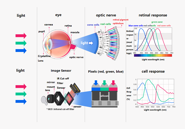
Figure. 1 Comparison between Human Eyes and CIS Response System
For images to be clearly visible in dark conditions, it is necessary to amplify signals from weak light while suppressing non-light signals (noise) as much as possible. In addition, to see clearly in a bright environment, a large amount of strong light needs to be received and distinguished. These features can be quantified by light intensity and DR (dynamic range: full trap capacity noise ratio) using the so-called SNR (comic-to-noise ratio).
In terms of dark light signal-to-noise ratio control, people have made a lot of efforts to amplify the signal while reducing unnecessary noise. Today, we are gradually raising these characteristics to the level of lux, which is a rather dark environment. In terms of dynamic range, the dynamic ranges within and between scenes of the human eye are usually 120 dB and 180 dB respectively. In the evolving state, the dynamic ranges in and between scenes of smartphones are currently 70 dB and 120 dB respectively.
The most important factor affecting the above characteristics is the size and resolution of the pixels. In order for CIS to achieve higher resolution, it is necessary to reduce the pixel size (pixel size). If CIS is to be placed on a smaller chip area at the same resolution, the pixel size must also be smaller. Keeping the above characteristics unchanged while reducing the pixel size is the most critical factor.
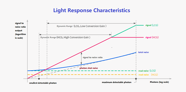
Figure. 2 Light Response Characteristics and Dynamic Range Extension
Ⅱ. How long will the battle between pixel size and resolution last?
The resolution of the human eye to the center of the still image is about 576 million pixels, and the resolution of the moving image is about 8 million pixels. CIS technology has been constantly improving to catch up with the human eye level. After reducing the pixel size to about 1.12μm and increasing the resolution to 13 million pixels, the development speed of CIS technology began to slow down, but the introduction of Quad technology (combining 2×2 pixels using the same color filter) once again accelerated the development of pixel size reduction. Recently, this level has reached the range of 0.7μm, and the resolution has also risen to 64 million pixels.
Today, with the development of NONA (3×3) and QxQ (4×4) technologies, the pixel size has reached the level in the range of 0.6Xμm. In turn, pixel size reduction technology has spawned the recently launched 108 million pixel resolution image sensors. With this development, people are increasingly looking forward to the launch of the 200-megapixel resolution camera in the near future.
Now we have caught up with many new developments. The reason why the above pixel binding technology is actively used is that we do not require high resolution when shooting videos. However, with the support of this new technology (pixel binding technology), camera s can now support uninterrupted recording of 4K (4000 x 2000: 8 megapixels) video at a speed of 60 frames per second. Pixel binding technology enables camera s to maintain the characteristics of large pixels in videos and provide excellent low-light sensitivity and dynamic range. In order to provide value-added services for customers, in the future, ultra-low light, dynamic range expansion technology, fast autofocus and other functions are expected to be added to video shooting.
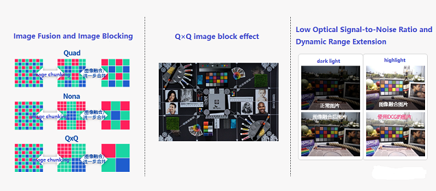
Figure. 3 Low Light SNR and Dynamic Range Extension Techniques
Reducing the size of image sensors (including reducing pixel sizes) is a common challenge for all semiconductor companies. In order to maintain the same functional characteristics on smaller sizes, these companies have carried out a lot of technical development work in equipment and manufacturing processes. Such technologies include doping optimization and vertical transfer gate - to improve full-well capacity (FWC) while maintaining charge transfer efficiency; source tracking engineering (source) Follower engineering and various noise reduction technologies; color filter isolation and deep trench isolation technology - between adjacent pixels Minimize interference; use a thick epitaxial layer (epi layer) to improve pixel sensitivity or apply various filter-related technologies, etc.
In terms of viewing images. today's semiconductors have achieved almost the same performance as the eyes of organisms that have evolved over millions of years through the above technologies. However, there is still the possibility of improvement in effectiveness. We are now witnessing the development of low-power technology: in standby mode, run with the lowest power consumption (so-called normally open mode) or optimize power consumption through compression sensing.
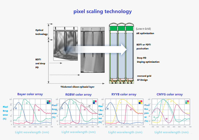
Figure. 4 Pixel Scaling Technique
Ⅲ. Beyond the human eye
In the process of expanding the application field of CIS. the most representative is deep sensing technology. Early CIS used two camera s to imitate the parallax of the human eye to sense the distance. However, people still need to work hard to break through the limitations of accuracy, distance scalability and minimum distance between the two cameras.
The method of measuring distance based on the time difference returned by light reflection from objects is called "Time of Flight" (ToF). ToF is divided into two types, direct flight time (dToF) and indirect flight time (iToF).
From the perspective of operation principle, each of these two methods has its own advantages and disadvantages. Indirect flight time sensing is based on the working principle of analog charge accumulation. Due to the long-distance attenuation of the signal, its measurable distance range is limited. Direct flight time is limited in resolution, because it is very difficult to detect the size of each single photon (SPAD: single photon avalanche diode) unit, and it also needs to be stacked in each unit to read out the circuit. In summary, these two methods can implement and take advantage of their own advantages in their respective applications, or strive to improve them to overcome their shortcomings.
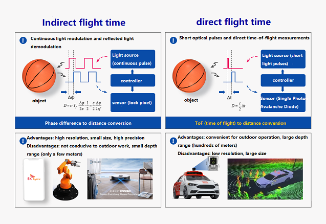
Figure. 5 Working Principle and Application Field of ToF Sensor
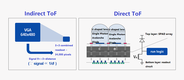
Figure. 6 Evolution of iToF and dToF
Based on broad-spectrum light, CIS uses visible light, ultraviolet light, near-infrared light, short-wave infrared light, etc. to expand its application field and make contributions to enriching human life. Ultraviolet and infrared wavelengths provide an opportunity to use alternative materials (such as Ge (Germanium), InGaAs (Indium Gallium Arsenic) and InP (Indium Phosphorus)) to solve the shortcomings of silicon. In addition, multispectral and hyperspectral imaging, or polarization sensors, have also begun to play a role.
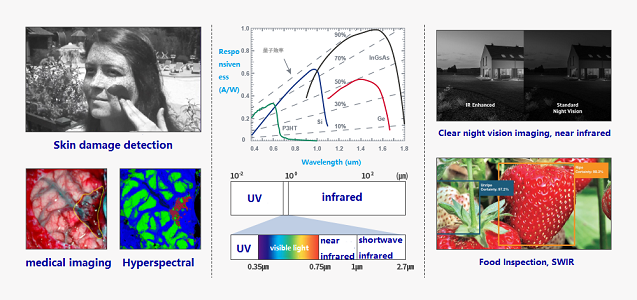
Figure 7 Expansion of image sensor application field
The widespread adoption of artificial intelligence (AI) in all walks of life has also brought benefits to the CIS industry. In the early stage, the technology mainly focused on noise reduction or resolution enhancement to improve the image itself, and is currently expanding to the field of object recognition and security. The widespread installation of cameras has raised concerns about privacy. While ensuring that the data needed for security is transmitted to the server, it is also necessary to prevent other data from being leaked. Therefore, AI functions will be migrated to edge devices, enabling us to reduce data transmission between Internet of Things devices while achieving energy saving. The use of infrared data and the emergence of event-driven sensors are also in line with this direction.
With the emergence of these sensors, a series of related technologies have also been further developed - new wearable devices such as over-ear monitors (HMD), AR/VR glasses, automated applications such as self-driving cars, robots and drones, and the integration and integration of different devices.
By providing image technology and sensing information about various lights, CIS will continue to make our lives more convenient and safe. SK Hynix is committed to continuously developing and following this trend, developing various products and creating more opportunities to add social value.
1. How many kinds are there in CMOS image sensors?
CMOS Passive Pixel Sensor(CMOS-PPS), CMOS active Pixel Sensor(CMOS- APS) and CMOS digital Pixel Sensor(CMOS- DPS). On this basis, CMOS vision sensor and CMOS Stress came out Sensor, log-polar CMOS Sensor, CMOS Retina Sensor, CMOS concave Sensor, log-transform CMOS image Sensor, track-to-track CMOS active pixel Sensor, single-slope mode CMOS image Sensor and CMOS fingerprint image Sensor, FoveonX3 panchromatic CMOS image Sensor, VMIS CMOS image sensor.
2. What is the output signal format of cmos image sensor
CMOS image sensor output RAW image format, some CMOS sensor also has JPEG image compression, can directly output JPEG image format. Image processing software can open RAW files and convert them to JPEG and other image files.
3. How do CMOS image sensors distinguish colors
CMOS image sensors distinguish colors through color filters on the sensor.
 The Key Role of Electronic Components in IoT DevicesUTMEL01 September 20235210
The article discusses the pivotal role of electronic components in Internet of Things (IoT) devices. IoT devices work by capturing real-world data using sensors, processing it through a microcontroller, and then sending it to the cloud for further analysis.
Read More How to Identify the Perfect Proximity Sensor for Your ApplicationUTMEL19 July 20251129
Find the best proximity sensors for your project by evaluating material, sensing range, environment, and system needs to ensure optimal performance and reliability.
Read More Trusted Vibration Sensors for Homeowners and Industry ProfessionalsUTMEL17 July 2025833
Compare top vibration sensors for home and industrial use. Find trusted options for security, predictive maintenance, and equipment protection.
Read More Wiring and Mounting Photoelectric Sensors in 2025UTMEL15 July 20251044
Wire and mount photoelectric sensors in 2025 with step-by-step safety, wiring, and alignment tips for reliable installation and optimal sensor performance.
Read More Essential Tips for Picking the Best Gas SensorUTMEL15 July 20252262
Find out how to select gas sensors by matching target gases, environment, and compliance needs for reliable and accurate gas detection in any setting.
Read More
Subscribe to Utmel !


 Product
 Brand
Brand Articles
 Tools
Tools


