

 Product
 Brand
Brand Articles
 Tools
Tools
The Future of Semiconductors: Chiplets and Super NoCs
The world of semiconductor implementation technology is on the brink of a major transformation. The advent of chiplets, multiple silicon dice mounted on a common substrate, is gaining traction among big players, with proprietary in-house implementations already in use. This shift promises to democratize chiplet technology, allowing everyone to participate in the future. Integrated circuits (ICs), circuits formed from a collection of components implemented on a small flat piece of semiconductor material, are commonly referred to as 'silicon chips.' These can be analog, digital, or mixed-signal in nature. The terms ASIC, ASSP, and SoC often cause confusion among the uninitiated. In simple terms, an ASIC is designed by and/or used by a single company in a specific system, an ASSP is a more general-purpose device created using ASIC tools and technologies for use by multiple system design houses, and an SoC is an ASIC or ASSP that acts as an entire subsystem. As semiconductor process technologies evolved, it became possible to squeeze more transistors into the same area and create larger chips. For instance, the Apple A16 Bionic, manufactured at the 4-nm process node, boasts over 15 billion transistors. However, we are reaching the limits of what can be achieved with current technologies. The solution lies in chiplets, multiple dice mounted on a common substrate, forming a multi-die system. Synopsys, a leading provider of high-quality, silicon-proven IP solutions for SoC designs, has identified four primary chiplet use cases. These include mounting multiple copies of the same die onto the substrate, splitting a design into two or more chiplets due to size and yield considerations, implementing main digital device functionality at the latest process node while using proven solutions for some input/output functions, and disaggregating the device functionality into multiple heterogeneous dice, each implemented at the optimal node for its function. However, the challenge lies in enabling chiplets to 'communicate' with each other using die-to-die (D2D) interconnect. Synopsys is partnering with Network-on-Chip (NoC) companies to develop 'Super NoCs' that offer the highest possible bandwidths with the lowest possible latency. NoCs are used to connect large IP blocks in a chip, allowing multiple packets passing between multiple IPs to be in flight at the same time. Arteris IP, a leading provider of network-on-chip interconnect IP solutions, has developed solutions for D2D implementations, considering factors such as cache coherency, protocol layer, link layer, and physical layer. The chiplet-based technology is still in its infancy, with research groups and industry partners working on design methodologies, communication interfaces, and tools to accelerate time to market. As the semiconductor industry continues to evolve, the future of IC design and implementation seems to be firmly rooted in chiplets and Super NoCs.
 UTMEL
UTMEL
We are the professional distributor of electronic components, providing a large variety of products to save you a lot of time, effort, and cost with our efficient self-customized service. careful order preparation fast delivery service
 Power Semiconductor Procurement After the Nexperia Shake-Up—NXP for Stability, ON for Technology, or Nexperia for Value?UTMEL04 November 20254828
The recent supply chain turmoil surrounding Netherlands-based Nexperia has sent shockwaves through the global semiconductor industry, forcing procurement professionals to re-evaluate their sourcing strategies.
Read More AI Computing Power Gap: How Token Consumption is Reshaping Server Component SourcingUTMEL23 June 2026898
As global token consumption drives the transition to high-density 100kW+ AI data centers, power delivery networks require advanced Wide-Bandgap semiconductors (SiC/GaN) and high-capacitance MLCCs. This shift has triggered a component procurement crisis with lead times exceeding 24 weeks. To bypass shortages, hardware buyers must abandon just-in-time manufacturing and leverage independent global distributor networks to secure critical power and passive components.
Read More The BSPDN Revolution: Overcoming IR Drop in Sub-2nm GAAFET Nodes with Backside Power DeliveryUTMEL25 June 2026818
As semiconductor manufacturing enters the sub-2nm era, Backside Power Delivery Networks (BSPDN) are replacing traditional front-side routing to overcome critical IR drop bottlenecks. By separating power and signal delivery, chipmakers like Intel and TSMC drastically improve performance and density in GAAFET designs. However, this radical shift introduces manufacturing complexities, thermal challenges, and demands advanced packaging and power management solutions.
Read More Power Management ICs Trends 2026: AI Demand, Supply Risks, and Sourcing StrategiesUTMEL06 July 20261300
As AI server racks surpass 100kW by 2026, data centers are shifting toward wide-bandgap semiconductors like SiC and GaN. However, this demand has triggered a critical shortage of mature-node Power Management ICs (PMICs). To prevent production halts, sourcing teams must abandon 'just-in-time' models, implement proactive 'just-in-case' strategies, and rapidly qualify pin-to-pin alternative components to secure their supply chains.
Read More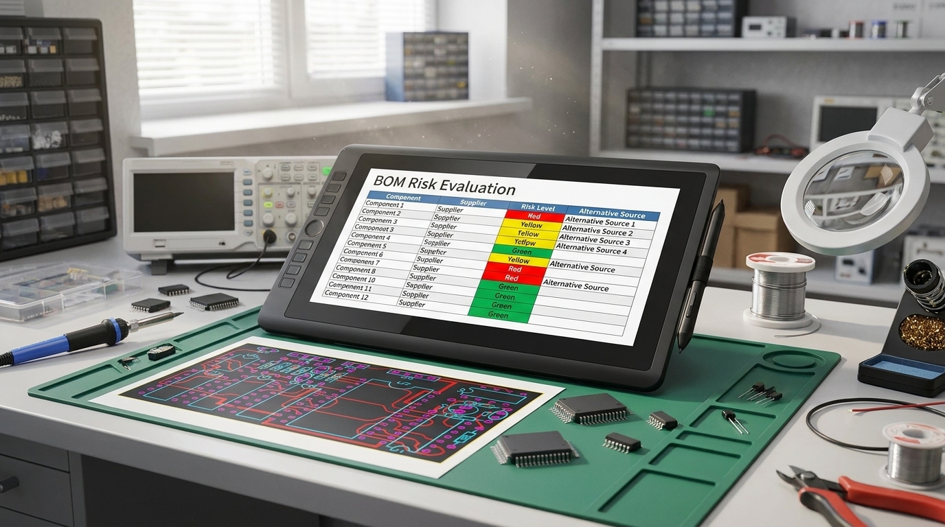 onsemi Synaptics Acquisition Impact: BOM Risk Checklist and Second-Source Strategy for Edge AI DesignsUTMEL27 July 2026296
The onsemi acquisition of Synaptics provides hardware program managers a 12-to-18-month window before potential product cancellations occur in mid-2027. This guide outlines how to audit BOM exposure across overlap and non-core product lines, calculate Last-Time-Buy volumes including hidden storage costs, establish proactive second-sourcing triggers, and implement supply chain monitoring to prevent line-down events.
Read More
Subscribe to Utmel !
![BLM18HE601SN1D]() BLM18HE601SN1D
BLM18HE601SN1DMurata Electronics
![CC1310F128RGZT]() CC1310F128RGZT
CC1310F128RGZTTexas Instruments
![NFM15PC435R0E3D]() NFM15PC435R0E3D
NFM15PC435R0E3DMurata Electronics
![NFM18PC104R1C3D]() NFM18PC104R1C3D
NFM18PC104R1C3DMurata Electronics
![PWT75]() PWT75
PWT75Panduit Corp
![PEC12R-2225F-N0024]() PEC12R-2225F-N0024
PEC12R-2225F-N0024Bourns Inc.
![BLM03BD471SN1D]() BLM03BD471SN1D
BLM03BD471SN1DMurata Electronics
![03453LS1HX020]() 03453LS1HX020
03453LS1HX020Littelfuse Inc.
![NFM21PC105B1C3D]() NFM21PC105B1C3D
NFM21PC105B1C3DMurata Electronics
![WC-620]() WC-620
WC-620JST Sales America Inc.


