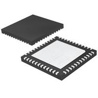

Linear Technology/Analog Devices LTC2222CUK-11#PBF
ADC 0.5mm Analog to Digital Converter
Manufacturer No:
LTC2222CUK-11#PBF
Tiny WHSLManufacturer:
Utmel No:
153-LTC2222CUK-11#PBF
Package:
48-WFQFN Exposed Pad
Datasheet:
Description:
12 Bit 0.5mm ADC LTC2222 3.3V 48-WFQFN Exposed Pad
Quantity:
Unit Price: $34.652070
Ext Price: $34.65
Delivery:


Payment:


In Stock : 12
Minimum: 1 Multiples: 1
Qty
Unit Price
Ext Price
1
$34.652070
$34.65
10
$32.690632
$326.91
100
$30.840219
$3,084.02
500
$29.094546
$14,547.27
1000
$27.447685
$27,447.68
Want a lower wholesale price? Please send RFQ, we will respond immediately.
RFQ Now
Add to RFQ list
You may place an order without registering to Utmel.
We strongly suggest you sign in before purchasing as you can track your order in real time.
For your convenience, we accept multiple payment methods in USD, including PayPal, Credit Card, and wire transfer.
RFQ (Request for Quotations)It is recommended to request for quotations to get the latest prices and inventories about the part.
Our sales will reply to your request by email within 24 hours.
1. You'll receive an order information email in your inbox. (Please remember to check the spam folder if you didn't hear from us).
2. Since inventories and prices may fluctuate to some extent, the sales manager is going to reconfirm the order and let you know if there are any updates.
- TypeParameter
- Factory Lead Time18 Weeks
- Mounting Type
The "Mounting Type" in electronic components refers to the method used to attach or connect a component to a circuit board or other substrate, such as through-hole, surface-mount, or panel mount.
Surface Mount - Package / Case
refers to the protective housing that encases an electronic component, providing mechanical support, electrical connections, and thermal management.
48-WFQFN Exposed Pad - Surface Mount
having leads that are designed to be soldered on the side of a circuit board that the body of the component is mounted on.
YES - Operating Temperature
The operating temperature is the range of ambient temperature within which a power supply, or any other electrical equipment, operate in. This ranges from a minimum operating temperature, to a peak or maximum operating temperature, outside which, the power supply may fail.
0°C~70°C - Packaging
Semiconductor package is a carrier / shell used to contain and cover one or more semiconductor components or integrated circuits. The material of the shell can be metal, plastic, glass or ceramic.
Tube - Published2005
- JESD-609 Code
The "JESD-609 Code" in electronic components refers to a standardized marking code that indicates the lead-free solder composition and finish of electronic components for compliance with environmental regulations.
e3 - Part Status
Parts can have many statuses as they progress through the configuration, analysis, review, and approval stages.
Active - Moisture Sensitivity Level (MSL)
Moisture Sensitivity Level (MSL) is a standardized rating that indicates the susceptibility of electronic components, particularly semiconductors, to moisture-induced damage during storage and the soldering process, defining the allowable exposure time to ambient conditions before they require special handling or baking to prevent failures
1 (Unlimited) - Number of Terminations48
- Terminal Finish
Terminal Finish refers to the surface treatment applied to the terminals or leads of electronic components to enhance their performance and longevity. It can improve solderability, corrosion resistance, and overall reliability of the connection in electronic assemblies. Common finishes include nickel, gold, and tin, each possessing distinct properties suitable for various applications. The choice of terminal finish can significantly impact the durability and effectiveness of electronic devices.
Matte Tin (Sn) - Terminal Position
In electronic components, the term "Terminal Position" refers to the physical location of the connection points on the component where external electrical connections can be made. These connection points, known as terminals, are typically used to attach wires, leads, or other components to the main body of the electronic component. The terminal position is important for ensuring proper connectivity and functionality of the component within a circuit. It is often specified in technical datasheets or component specifications to help designers and engineers understand how to properly integrate the component into their circuit designs.
QUAD - Terminal Form
Occurring at or forming the end of a series, succession, or the like; closing; concluding.
NO LEAD - Peak Reflow Temperature (Cel)
Peak Reflow Temperature (Cel) is a parameter that specifies the maximum temperature at which an electronic component can be exposed during the reflow soldering process. Reflow soldering is a common method used to attach electronic components to a circuit board. The Peak Reflow Temperature is crucial because it ensures that the component is not damaged or degraded during the soldering process. Exceeding the specified Peak Reflow Temperature can lead to issues such as component failure, reduced performance, or even permanent damage to the component. It is important for manufacturers and assemblers to adhere to the recommended Peak Reflow Temperature to ensure the reliability and functionality of the electronic components.
260 - Number of Functions1
- Supply Voltage
Supply voltage refers to the electrical potential difference provided to an electronic component or circuit. It is crucial for the proper operation of devices, as it powers their functions and determines performance characteristics. The supply voltage must be within specified limits to ensure reliability and prevent damage to components. Different electronic devices have specific supply voltage requirements, which can vary widely depending on their design and intended application.
3.3V - Terminal Pitch
The center distance from one pole to the next.
0.5mm - Time@Peak Reflow Temperature-Max (s)
Time@Peak Reflow Temperature-Max (s) refers to the maximum duration that an electronic component can be exposed to the peak reflow temperature during the soldering process, which is crucial for ensuring reliable solder joint formation without damaging the component.
30 - Base Part Number
The "Base Part Number" (BPN) in electronic components serves a similar purpose to the "Base Product Number." It refers to the primary identifier for a component that captures the essential characteristics shared by a group of similar components. The BPN provides a fundamental way to reference a family or series of components without specifying all the variations and specific details.
LTC2222 - Pin Count
a count of all of the component leads (or pins)
48 - JESD-30 Code
JESD-30 Code refers to a standardized descriptive designation system established by JEDEC for semiconductor-device packages. This system provides a systematic method for generating designators that convey essential information about the package's physical characteristics, such as size and shape, which aids in component identification and selection. By using JESD-30 codes, manufacturers and engineers can ensure consistency and clarity in the specification of semiconductor packages across various applications and industries.
S-PQCC-N48 - Qualification Status
An indicator of formal certification of qualifications.
Not Qualified - Power Supplies
an electronic circuit that converts the voltage of an alternating current (AC) into a direct current (DC) voltage.?
3.3V - Configuration
The parameter "Configuration" in electronic components refers to the specific arrangement or setup of the components within a circuit or system. It encompasses how individual elements are interconnected and their physical layout. Configuration can affect the functionality, performance, and efficiency of the electronic system, and may influence factors such as signal flow, impedance, and power distribution. Understanding the configuration is essential for design, troubleshooting, and optimizing electronic devices.
S/H-ADC - Number of Bits12
- Input Type
Input type in electronic components refers to the classification of the signal or data that a component can accept for processing or conversion. It indicates whether the input is analog, digital, or a specific format such as TTL or CMOS. Understanding input type is crucial for ensuring compatibility between different electronic devices and circuits, as it determines how signals are interpreted and interacted with.
Differential, Single Ended - Architecture
In electronic components, the parameter "Architecture" refers to the overall design and structure of the component. It encompasses the arrangement of internal components, the layout of circuitry, and the physical form of the component. The architecture of an electronic component plays a crucial role in determining its functionality, performance, and compatibility with other components in a system. Different architectures can result in variations in power consumption, speed, size, and other key characteristics of the component. Designers often consider the architecture of electronic components carefully to ensure optimal performance and integration within a larger system.
Pipelined - Number of Inputs1
- Converter Type
The parameter "Converter Type" in electronic components refers to the classification of devices that convert one form of energy or signal to another. This includes devices such as analog-to-digital converters (ADCs), digital-to-analog converters (DACs), and various types of signal converters used in communication, power management, and measurement systems. Each converter type is designed to facilitate the manipulation or transformation of signals to meet specific application requirements. The choice of converter type typically depends on factors such as the signal characteristics, required accuracy, and conversion speed.
ADC, PROPRIETARY METHOD - Reference Type
a code object that is not stored directly where it is created, but that acts as a kind of pointer to a value stored elsewhere.
External, Internal - Data Interface
A Data Interface in EDQ is a template of a set of attributes representing a given entity, used to create processes that read from, or write to, interfaces rather than directly from or to sources or targets of data.
LVDS - Parallel, Parallel - Voltage - Supply, Analog
Voltage - Supply, Analog is a parameter in electronic components that specifies the range of voltage levels required to power the analog circuitry within the component. This parameter indicates the minimum and maximum voltage levels that the component can accept for proper operation of its analog functions. It is crucial to ensure that the voltage supplied to the component falls within this specified range to prevent damage and ensure optimal performance. Understanding and adhering to the "Voltage - Supply, Analog" parameter is essential for the proper functioning of analog circuits in electronic components.
3.1V~3.5V - Voltage - Supply, Digital
Voltage - Supply, Digital is a parameter that specifies the voltage level required to power the digital circuitry within an electronic component, such as an integrated circuit or a microcontroller. This parameter is crucial for ensuring proper operation of the digital components, as supplying the correct voltage level is essential for reliable performance. The specified voltage range typically includes both minimum and maximum values within which the component can operate safely and efficiently. It is important to adhere to the recommended voltage supply range to prevent damage to the component and to maintain the integrity of the digital signals being processed.
3.1V~3.5V - Number of Analog In Channels1
- Sampling Rate (Per Second)
The sampling rate (per second) in electronic components refers to the frequency at which an analog signal is measured or sampled to convert it into a digital signal. It is typically expressed in Hertz (Hz) and indicates how many times per second the analog signal is sampled. A higher sampling rate allows for better representation of the original signal, capturing more detail and reducing distortion during the conversion process. In audio applications, for example, common sampling rates include 44.1 kHz for CD-quality audio and 48 kHz for video production.
105M - Output Bit Code
Output Bit Code refers to the digital representation of the output signal of an electronic component, typically in binary form. It indicates the specific combination of bits that represent the output value of the component. The output bit code is crucial for interpreting and processing the output data accurately in digital systems. By understanding the output bit code, engineers can design appropriate circuits and algorithms to manipulate and utilize the output information effectively.
OFFSET BINARY, 2'S COMPLEMENT BINARY - Linearity Error-Max (EL)
Linearity Error-Max (EL) is a parameter used to quantify the deviation of a device's output from a straight line response over its specified input range. It measures the maximum difference between the ideal output and the actual output of the component when subjected to varying input levels. A smaller linearity error indicates better performance, as it signifies more accurate and consistent output behavior across the input spectrum. This parameter is critical in applications requiring precision, such as analog-to-digital converters and other signal processing components.
0.049% - Sample and Hold / Track and Hold
"Sample and Hold" and "Track and Hold" are two related functions commonly found in electronic components such as analog-to-digital converters (ADCs) and signal processing circuits. In a Sample and Hold circuit, the input signal is sampled at specific intervals and held constant until the next sampling period. This allows the circuit to capture and store the input signal's value for further processing or conversion.On the other hand, a Track and Hold circuit continuously tracks the input signal's value and holds it steady when required, typically during the conversion process. This ensures that the input signal remains constant and accurate during the conversion process.Both functions are essential in maintaining the integrity and accuracy of analog signals in digital systems, allowing for precise measurements and processing of signals in various electronic applications.
SAMPLE - Ratio - S/H:ADC
The parameter "Ratio - S/H:ADC" in electronic components refers to the ratio between the sample and hold (S/H) circuit and the analog-to-digital converter (ADC) in a system. The sample and hold circuit is responsible for capturing and holding the input signal at a specific moment in time, while the ADC converts this analog signal into a digital format for processing. The ratio between the S/H and ADC components is important as it determines the accuracy and speed of the analog-to-digital conversion process. A higher ratio typically indicates a more precise and efficient conversion process, leading to better overall performance of the electronic system. Engineers often consider this parameter when designing and optimizing electronic circuits to ensure reliable and high-quality signal processing.
1:1 - Analog Input Voltage-Max
Analog Input Voltage-Max refers to the maximum voltage level that can be safely applied to the input of an electronic component, such as an integrated circuit or sensor, without causing damage. This parameter is crucial for ensuring the proper functioning and longevity of the component. Exceeding the specified maximum input voltage can lead to overloading, overheating, or even permanent damage to the component. It is important for designers and engineers to carefully consider and adhere to this parameter when designing circuits or systems to prevent potential failures and ensure reliable operation.
1V - Output Format
Output formats are used to determine which data is exported and how data is displayed in many areas of OLIB.
PARALLEL, WORD - Length7mm
- Height Seated (Max)
Height Seated (Max) is a parameter in electronic components that refers to the maximum allowable height of the component when it is properly seated or installed on a circuit board or within an enclosure. This specification is crucial for ensuring proper fit and alignment within the overall system design. Exceeding the maximum seated height can lead to mechanical interference, electrical shorts, or other issues that may impact the performance and reliability of the electronic device. Manufacturers provide this information to help designers and engineers select components that will fit within the designated space and function correctly in the intended application.
0.8mm - Width7mm
- RoHS Status
RoHS means “Restriction of Certain Hazardous Substances” in the “Hazardous Substances Directive” in electrical and electronic equipment.
ROHS3 Compliant


