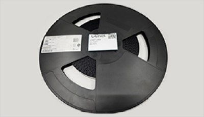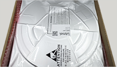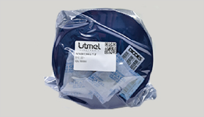

Maxim Integrated MAX319CSA T
Multiplexers ICs 15V SPDT 175ns, 145ns Analog Switches 8 Pins
Manufacturer No:
MAX319CSA T
Tiny WHSLManufacturer:
Utmel No:
1551-MAX319CSA T
Package:
8-SOIC (0.154, 3.90mm Width)
Description:
175ns, 145ns SPDT 35Ohm Analog Switches BREAK-BEFORE-MAKE MAX319 8 Pins 250pA 15V 8-SOIC (0.154, 3.90mm Width)
Quantity:
Unit Price: $12.285575
Ext Price: $12.29
Delivery:


Payment:


In Stock : 6800
Minimum: 1 Multiples: 1
Qty
Unit Price
Ext Price
1
$12.285575
$12.29
10
$11.590165
$115.90
100
$10.934118
$1,093.41
500
$10.315206
$5,157.60
1000
$9.731326
$9,731.33
Want a lower wholesale price? Please send RFQ, we will respond immediately.
RFQ Now
Add to RFQ list
You may place an order without registering to Utmel.
We strongly suggest you sign in before purchasing as you can track your order in real time.
For your convenience, we accept multiple payment methods in USD, including PayPal, Credit Card, and wire transfer.
RFQ (Request for Quotations)It is recommended to request for quotations to get the latest prices and inventories about the part.
Our sales will reply to your request by email within 24 hours.
1. You'll receive an order information email in your inbox. (Please remember to check the spam folder if you didn't hear from us).
2. Since inventories and prices may fluctuate to some extent, the sales manager is going to reconfirm the order and let you know if there are any updates.
- TypeParameter
- Factory Lead Time6 Weeks
- Mount
In electronic components, the term "Mount" typically refers to the method or process of physically attaching or fixing a component onto a circuit board or other electronic device. This can involve soldering, adhesive bonding, or other techniques to secure the component in place. The mounting process is crucial for ensuring proper electrical connections and mechanical stability within the electronic system. Different components may have specific mounting requirements based on their size, shape, and function, and manufacturers provide guidelines for proper mounting procedures to ensure optimal performance and reliability of the electronic device.
Surface Mount - Mounting Type
The "Mounting Type" in electronic components refers to the method used to attach or connect a component to a circuit board or other substrate, such as through-hole, surface-mount, or panel mount.
Surface Mount - Package / Case
refers to the protective housing that encases an electronic component, providing mechanical support, electrical connections, and thermal management.
8-SOIC (0.154, 3.90mm Width) - Number of Pins8
- Turn Off Delay Time
It is the time from when Vgs drops below 90% of the gate drive voltage to when the drain current drops below 90% of the load current. It is the delay before current starts to transition in the load, and depends on Rg. Ciss.
145 ns - Published1995
- Packaging
Semiconductor package is a carrier / shell used to contain and cover one or more semiconductor components or integrated circuits. The material of the shell can be metal, plastic, glass or ceramic.
Tape & Reel (TR) - Operating Temperature
The operating temperature is the range of ambient temperature within which a power supply, or any other electrical equipment, operate in. This ranges from a minimum operating temperature, to a peak or maximum operating temperature, outside which, the power supply may fail.
0°C~70°C TA - JESD-609 Code
The "JESD-609 Code" in electronic components refers to a standardized marking code that indicates the lead-free solder composition and finish of electronic components for compliance with environmental regulations.
e3 - Pbfree Code
The "Pbfree Code" parameter in electronic components refers to the code or marking used to indicate that the component is lead-free. Lead (Pb) is a toxic substance that has been widely used in electronic components for many years, but due to environmental concerns, there has been a shift towards lead-free alternatives. The Pbfree Code helps manufacturers and users easily identify components that do not contain lead, ensuring compliance with regulations and promoting environmentally friendly practices. It is important to pay attention to the Pbfree Code when selecting electronic components to ensure they meet the necessary requirements for lead-free applications.
yes - Part Status
Parts can have many statuses as they progress through the configuration, analysis, review, and approval stages.
Active - Moisture Sensitivity Level (MSL)
Moisture Sensitivity Level (MSL) is a standardized rating that indicates the susceptibility of electronic components, particularly semiconductors, to moisture-induced damage during storage and the soldering process, defining the allowable exposure time to ambient conditions before they require special handling or baking to prevent failures
1 (Unlimited) - Number of Terminations8
- ECCN Code
An ECCN (Export Control Classification Number) is an alphanumeric code used by the U.S. Bureau of Industry and Security to identify and categorize electronic components and other dual-use items that may require an export license based on their technical characteristics and potential for military use.
EAR99 - Resistance
Resistance is a fundamental property of electronic components that measures their opposition to the flow of electric current. It is denoted by the symbol "R" and is measured in ohms (Ω). Resistance is caused by the collisions of electrons with atoms in a material, which generates heat and reduces the flow of current. Components with higher resistance will impede the flow of current more than those with lower resistance. Resistance plays a crucial role in determining the behavior and functionality of electronic circuits, such as limiting current flow, voltage division, and controlling power dissipation.
35Ohm - Terminal Finish
Terminal Finish refers to the surface treatment applied to the terminals or leads of electronic components to enhance their performance and longevity. It can improve solderability, corrosion resistance, and overall reliability of the connection in electronic assemblies. Common finishes include nickel, gold, and tin, each possessing distinct properties suitable for various applications. The choice of terminal finish can significantly impact the durability and effectiveness of electronic devices.
Matte Tin (Sn) - Max Power Dissipation
The maximum power that the MOSFET can dissipate continuously under the specified thermal conditions.
471mW - Terminal Form
Occurring at or forming the end of a series, succession, or the like; closing; concluding.
GULL WING - Peak Reflow Temperature (Cel)
Peak Reflow Temperature (Cel) is a parameter that specifies the maximum temperature at which an electronic component can be exposed during the reflow soldering process. Reflow soldering is a common method used to attach electronic components to a circuit board. The Peak Reflow Temperature is crucial because it ensures that the component is not damaged or degraded during the soldering process. Exceeding the specified Peak Reflow Temperature can lead to issues such as component failure, reduced performance, or even permanent damage to the component. It is important for manufacturers and assemblers to adhere to the recommended Peak Reflow Temperature to ensure the reliability and functionality of the electronic components.
260 - Number of Functions1
- Supply Voltage
Supply voltage refers to the electrical potential difference provided to an electronic component or circuit. It is crucial for the proper operation of devices, as it powers their functions and determines performance characteristics. The supply voltage must be within specified limits to ensure reliability and prevent damage to components. Different electronic devices have specific supply voltage requirements, which can vary widely depending on their design and intended application.
15V - Base Part Number
The "Base Part Number" (BPN) in electronic components serves a similar purpose to the "Base Product Number." It refers to the primary identifier for a component that captures the essential characteristics shared by a group of similar components. The BPN provides a fundamental way to reference a family or series of components without specifying all the variations and specific details.
MAX319 - Pin Count
a count of all of the component leads (or pins)
8 - Operating Supply Voltage
The voltage level by which an electrical system is designated and to which certain operating characteristics of the system are related.
20V - Number of Channels1
- Number of Circuits1
- Max Supply Voltage
In general, the absolute maximum common-mode voltage is VEE-0.3V and VCC+0.3V, but for products without a protection element at the VCC side, voltages up to the absolute maximum rated supply voltage (i.e. VEE+36V) can be supplied, regardless of supply voltage.
30V - Min Supply Voltage
The minimum supply voltage (V min ) is explored for sequential logic circuits by statistically simulating the impact of within-die process variations and gate-dielectric soft breakdown on data retention and hold time.
10V - Operating Supply Current
Operating Supply Current, also known as supply current or quiescent current, is a crucial parameter in electronic components that indicates the amount of current required for the device to operate under normal conditions. It represents the current drawn by the component from the power supply while it is functioning. This parameter is important for determining the power consumption of the component and is typically specified in datasheets to help designers calculate the overall power requirements of their circuits. Understanding the operating supply current is essential for ensuring proper functionality and efficiency of electronic systems.
1μA - Nominal Supply Current
Nominal current is the same as the rated current. It is the current drawn by the motor while delivering rated mechanical output at its shaft.
100pA - Max Supply Current
Max Supply Current refers to the maximum amount of electrical current that a component can draw from its power supply under normal operating conditions. It is a critical parameter that ensures the component operates reliably without exceeding its thermal limits or damaging internal circuitry. Exceeding this current can lead to overheating, performance degradation, or failure of the component. Understanding this parameter is essential for designing circuits that provide adequate power while avoiding overload situations.
100pA - Turn On Delay Time
Turn-on delay, td(on), is the time taken to charge the input capacitance of the device before drain current conduction can start.
175 ns - Voltage - Supply, Single/Dual (±)
The parameter "Voltage - Supply, Single/Dual (±)" in electronic components refers to the power supply voltage required for the proper operation of the component. This parameter indicates whether the component requires a single power supply voltage (e.g., 5V) or a dual power supply voltage (e.g., ±15V). For components that require a single power supply voltage, only one voltage level is needed for operation. On the other hand, components that require a dual power supply voltage need both positive and negative voltage levels to function correctly.Understanding the voltage supply requirements of electronic components is crucial for designing and integrating them into circuits to ensure proper functionality and prevent damage due to incorrect voltage levels.
10V~30V ±4.5V~20V - Supply Type
Supply Type in electronic components refers to the classification of power sources used to operate the component. It indicates whether the component requires DC or AC power, and if DC, specifies the voltage levels such as low, medium, or high. Different supply types can affect the performance, compatibility, and application of the component in electronic circuits. Understanding the supply type is crucial for proper component selection and integration into electronic designs.
Dual, Single - Neg Supply Voltage-Nom (Vsup)
The parameter "Neg Supply Voltage-Nom (Vsup)" in electronic components refers to the nominal negative supply voltage that the component requires to operate within its specified performance characteristics. This parameter indicates the minimum voltage level that must be provided to the component's negative supply pin for proper functionality. It is important to ensure that the negative supply voltage provided to the component does not exceed the maximum specified value to prevent damage or malfunction. Understanding and adhering to the specified negative supply voltage requirements is crucial for the reliable operation of the electronic component in a circuit.
-15V - Max Dual Supply Voltage
A Dual power supply is a regular direct current power supply. It can provide a positive as well as negative voltage. It ensures stable power supply to the device as well as it helps to prevent system damage.
20V - On-State Resistance (Max)
The "On-State Resistance (Max)" parameter in electronic components refers to the maximum resistance exhibited by the component when it is in the fully conducting state. This resistance is typically measured when the component is carrying the maximum specified current. A lower on-state resistance indicates better conductivity and efficiency of the component when it is in the on-state. It is an important parameter to consider when selecting components for applications where low power dissipation and high efficiency are critical factors.
35Ohm - Min Dual Supply Voltage
The parameter "Min Dual Supply Voltage" in electronic components refers to the minimum voltage required for the proper operation of a device that uses dual power supplies. Dual power supplies typically consist of a positive and a negative voltage source. The "Min Dual Supply Voltage" specification ensures that both the positive and negative supply voltages are within a certain range to guarantee the device functions correctly. It is important to adhere to this parameter to prevent damage to the component and ensure reliable performance.
4.5V - Multiplexer/Demultiplexer Circuit
A Multiplexer/Demultiplexer Circuit is an electronic component used in digital circuits to select one of several input signals and route it to a single output. A multiplexer, also known as a "mux," is used to combine multiple input signals into a single output, while a demultiplexer, also known as a "demux," is used to take a single input and route it to one of several possible outputs. These circuits are commonly used in data transmission, communication systems, and digital signal processing applications to efficiently manage and control the flow of data. Multiplexers and demultiplexers play a crucial role in optimizing the use of resources and improving the overall performance of electronic systems.
2:1 - Off-state Isolation-Nom
Off-state Isolation-Nom is a parameter used to measure the level of isolation between two electronic components or circuits when one of them is in the off state. It indicates the ability of the component to prevent unwanted signals or interference from passing through when it is not actively conducting. The parameter is typically expressed in decibels (dB) and is an important consideration in designing and selecting components for applications where isolation between different parts of a circuit is critical to prevent crosstalk or interference. Higher values of Off-state Isolation-Nom indicate better isolation performance, leading to improved overall system reliability and performance.
68 dB - Current - Leakage (IS(off)) (Max)
Current - Leakage (IS(off)) (Max) refers to the maximum amount of current that flows through a device when it is in its off state, meaning it is not conducting or not intended to be active. This parameter is crucial in determining the efficiency of electronic components, especially in battery-operated devices, as higher leakage currents can lead to increased power consumption and reduced battery life. It is typically measured in microamperes (µA) or milliamperes (mA) and helps engineers assess the suitability of a component for low-power applications.
250pA - Channel Capacitance (CS(off), CD(off))
Channel capacitance (CS(off), CD(off)) in electronic components refers to the capacitance associated with the channel of a field-effect transistor (FET) when it is turned off. CS(off) represents the capacitance between the source and the gate of the FET, while CD(off) represents the capacitance between the drain and the gate. These capacitances play a crucial role in determining the high-frequency performance and switching characteristics of the FET. Understanding and controlling these capacitances is essential for optimizing the performance of electronic circuits, especially in high-speed applications where minimizing parasitic capacitances is critical for achieving desired signal integrity and efficiency.
8pF 8pF - On-state Resistance Match-Nom
On-state Resistance Match-Nom refers to the nominal or standard value of the on-state resistance for a specific electronic component, such as a transistor or a MOSFET, when it is in its "on" state. This parameter indicates how much resistance the component presents to current flow during its conducting phase, which affects power dissipation and efficiency. Matching this value across multiple devices is crucial for ensuring consistent performance in applications where several components operate together.
2Ohm - Switch Circuit
establishes connections between links, on demand and as available, in order to establish an end-to-end circuit between devices.
SPDT - Switch Time (Ton, Toff) (Max)
The parameter "Switch Time (Ton, Toff) (Max)" in electronic components refers to the maximum time it takes for a device to transition between its on and off states. Ton represents the turn-on time, which is the time taken for the device to switch from the off state to the on state, while Toff represents the turn-off time, which is the time taken for the device to switch from the on state to the off state. This parameter is crucial in determining the speed and efficiency of the device's switching operation. A shorter switch time generally indicates faster switching speeds and better performance of the electronic component.
175ns, 145ns - Charge Injection
A Charge injection in analog switches and multiplexers is a level change caused by stray capacitance associated with the NMOS and PMOS transistors that make up the analog switch.
3pC - Channel-to-Channel Matching (ΔRon)
Channel-to-Channel Matching (ΔRon) refers to the variation in the on-resistance of multiple channels within a multi-channel electronic component, such as a multiplexer or a switch. It is a measure of how closely the on-resistance values of different channels match each other. The lower the ΔRon value, the better the matching between channels, which is important for ensuring consistent performance across all channels in a system. Channel-to-Channel Matching is critical in applications where precise and uniform signal processing is required, such as in instrumentation, audio equipment, and communication systems. Manufacturers provide specifications for ΔRon to help designers select components that meet their performance requirements.
2 Ω (Max) - Switching
In electronic components, "Switching" refers to the process of turning a device on or off, or changing its state from one condition to another. This parameter is crucial in determining the speed and efficiency of a component's operation. It is often measured in terms of switching time, which is the time taken for a device to transition from one state to another. The switching characteristics of a component play a significant role in its overall performance and reliability in electronic circuits.
BREAK-BEFORE-MAKE - Length4.9mm
- Width3.9mm
- RoHS Status
RoHS means “Restriction of Certain Hazardous Substances” in the “Hazardous Substances Directive” in electrical and electronic equipment.
ROHS3 Compliant - Radiation Hardening
Radiation hardening is the process of making electronic components and circuits resistant to damage or malfunction caused by high levels of ionizing radiation, especially for environments in outer space (especially beyond the low Earth orbit), around nuclear reactors and particle accelerators, or during nuclear accidents or nuclear warfare.
No - REACH SVHC
The parameter "REACH SVHC" in electronic components refers to the compliance with the Registration, Evaluation, Authorization, and Restriction of Chemicals (REACH) regulation regarding Substances of Very High Concern (SVHC). SVHCs are substances that may have serious effects on human health or the environment, and their use is regulated under REACH to ensure their safe handling and minimize their impact.Manufacturers of electronic components need to declare if their products contain any SVHCs above a certain threshold concentration and provide information on the safe use of these substances. This information allows customers to make informed decisions about the potential risks associated with using the components and take appropriate measures to mitigate any hazards.Ensuring compliance with REACH SVHC requirements is essential for electronics manufacturers to meet regulatory standards, protect human health and the environment, and maintain transparency in their supply chain. It also demonstrates a commitment to sustainability and responsible manufacturing practices in the electronics industry.
Unknown - Lead Free
Lead Free is a term used to describe electronic components that do not contain lead as part of their composition. Lead is a toxic material that can have harmful effects on human health and the environment, so the electronics industry has been moving towards lead-free components to reduce these risks. Lead-free components are typically made using alternative materials such as silver, copper, and tin. Manufacturers must comply with regulations such as the Restriction of Hazardous Substances (RoHS) directive to ensure that their products are lead-free and environmentally friendly.
Lead Free
![LTC2634CUD-LMX12#PBF]()
LTC2634CUD-LMX12#PBF
Analog Devices![LTC2637IDE-HMI8#PBF]()
LTC2637IDE-HMI8#PBF
Analog Devices![LT3094IDD#TRPBF]()
LT3094IDD#TRPBF
Analog Devices![LTC6993CS6-3#TRPBF]()
LTC6993CS6-3#TRPBF
Analog Devices![LTC3838IFE#TRPBF]()
LTC3838IFE#TRPBF
Analog Devices![LTC4162IUFD-SST#TRPBF]()
LTC4162IUFD-SST#TRPBF
Analog Devices![LTC3374AIFE#PBF]()
LTC3374AIFE#PBF
Analog Devices![LT8606BEDC#TRPBF]()
LT8606BEDC#TRPBF
Analog Devices![LTC4121EUD#PBF]()
LTC4121EUD#PBF
Analog Devices![LT3066EDE-3.3#TRPBF]()
LT3066EDE-3.3#TRPBF
Analog Devices


