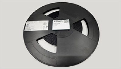
ON Semiconductor H11F3SR2VM
Manufacturer No:
H11F3SR2VM
Tiny WHSLManufacturer:
Utmel No:
1807-H11F3SR2VM
Package:
6-SMD, Gull Wing
Datasheet:
Description:
OPTOISOLTR 7.5KV PHOTO FET 6-SMD
Quantity:
Unit Price: $3.324995
Ext Price: $3.32
Delivery:


Payment:


In Stock : 20000
Minimum: 1 Multiples: 1
Qty
Unit Price
Ext Price
1
$3.324995
$3.32
10
$3.136788
$31.37
100
$2.959234
$295.92
500
$2.791730
$1,395.86
1000
$2.633707
$2,633.71
Want a lower wholesale price? Please send RFQ, we will respond immediately.
RFQ Now
Add to RFQ list
You may place an order without registering to Utmel.
We strongly suggest you sign in before purchasing as you can track your order in real time.
For your convenience, we accept multiple payment methods in USD, including PayPal, Credit Card, and wire transfer.
RFQ (Request for Quotations)It is recommended to request for quotations to get the latest prices and inventories about the part.
Our sales will reply to your request by email within 24 hours.
1. You'll receive an order information email in your inbox. (Please remember to check the spam folder if you didn't hear from us).
2. Since inventories and prices may fluctuate to some extent, the sales manager is going to reconfirm the order and let you know if there are any updates.
- TypeParameter
- Lifecycle Status
Lifecycle Status refers to the current stage of an electronic component in its product life cycle, indicating whether it is active, obsolete, or transitioning between these states. An active status means the component is in production and available for purchase. An obsolete status indicates that the component is no longer being manufactured or supported, and manufacturers typically provide a limited time frame for support. Understanding the lifecycle status is crucial for design engineers to ensure continuity and reliability in their projects.
ACTIVE (Last Updated: 2 weeks ago) - Factory Lead Time7 Weeks
- Mount
In electronic components, the term "Mount" typically refers to the method or process of physically attaching or fixing a component onto a circuit board or other electronic device. This can involve soldering, adhesive bonding, or other techniques to secure the component in place. The mounting process is crucial for ensuring proper electrical connections and mechanical stability within the electronic system. Different components may have specific mounting requirements based on their size, shape, and function, and manufacturers provide guidelines for proper mounting procedures to ensure optimal performance and reliability of the electronic device.
Surface Mount - Mounting Type
The "Mounting Type" in electronic components refers to the method used to attach or connect a component to a circuit board or other substrate, such as through-hole, surface-mount, or panel mount.
Surface Mount - Package / Case
refers to the protective housing that encases an electronic component, providing mechanical support, electrical connections, and thermal management.
6-SMD, Gull Wing - Number of Pins6
- Weight810mg
- Number of Elements1
- Operating Temperature
The operating temperature is the range of ambient temperature within which a power supply, or any other electrical equipment, operate in. This ranges from a minimum operating temperature, to a peak or maximum operating temperature, outside which, the power supply may fail.
-40°C~100°C - Packaging
Semiconductor package is a carrier / shell used to contain and cover one or more semiconductor components or integrated circuits. The material of the shell can be metal, plastic, glass or ceramic.
Tape & Reel (TR) - Published2008
- JESD-609 Code
The "JESD-609 Code" in electronic components refers to a standardized marking code that indicates the lead-free solder composition and finish of electronic components for compliance with environmental regulations.
e3 - Pbfree Code
The "Pbfree Code" parameter in electronic components refers to the code or marking used to indicate that the component is lead-free. Lead (Pb) is a toxic substance that has been widely used in electronic components for many years, but due to environmental concerns, there has been a shift towards lead-free alternatives. The Pbfree Code helps manufacturers and users easily identify components that do not contain lead, ensuring compliance with regulations and promoting environmentally friendly practices. It is important to pay attention to the Pbfree Code when selecting electronic components to ensure they meet the necessary requirements for lead-free applications.
yes - Part Status
Parts can have many statuses as they progress through the configuration, analysis, review, and approval stages.
Active - Moisture Sensitivity Level (MSL)
Moisture Sensitivity Level (MSL) is a standardized rating that indicates the susceptibility of electronic components, particularly semiconductors, to moisture-induced damage during storage and the soldering process, defining the allowable exposure time to ambient conditions before they require special handling or baking to prevent failures
1 (Unlimited) - ECCN Code
An ECCN (Export Control Classification Number) is an alphanumeric code used by the U.S. Bureau of Industry and Security to identify and categorize electronic components and other dual-use items that may require an export license based on their technical characteristics and potential for military use.
EAR99 - Terminal Finish
Terminal Finish refers to the surface treatment applied to the terminals or leads of electronic components to enhance their performance and longevity. It can improve solderability, corrosion resistance, and overall reliability of the connection in electronic assemblies. Common finishes include nickel, gold, and tin, each possessing distinct properties suitable for various applications. The choice of terminal finish can significantly impact the durability and effectiveness of electronic devices.
Tin (Sn) - Additional Feature
Any Feature, including a modified Existing Feature, that is not an Existing Feature.
UL RECOGNIZED, VDE APPROVED - Max Power Dissipation
The maximum power that the MOSFET can dissipate continuously under the specified thermal conditions.
300mW - Voltage - Isolation
Voltage - Isolation is a parameter in electronic components that refers to the maximum voltage that can be safely applied between two isolated points without causing electrical breakdown or leakage. It is a crucial specification for components such as transformers, optocouplers, and capacitors that require isolation to prevent electrical interference or safety hazards. The voltage isolation rating ensures that the component can withstand the specified voltage without compromising its performance or safety. It is typically measured in volts and is an important consideration when designing circuits that require isolation between different parts of the system.
7500Vpk - Output Type
The "Output Type" parameter in electronic components refers to the type of signal or data that is produced by the component as an output. This parameter specifies the nature of the output signal, such as analog or digital, and can also include details about the voltage levels, current levels, frequency, and other characteristics of the output signal. Understanding the output type of a component is crucial for ensuring compatibility with other components in a circuit or system, as well as for determining how the output signal can be utilized or processed further. In summary, the output type parameter provides essential information about the nature of the signal that is generated by the electronic component as its output.
MOSFET - Configuration
The parameter "Configuration" in electronic components refers to the specific arrangement or setup of the components within a circuit or system. It encompasses how individual elements are interconnected and their physical layout. Configuration can affect the functionality, performance, and efficiency of the electronic system, and may influence factors such as signal flow, impedance, and power distribution. Understanding the configuration is essential for design, troubleshooting, and optimizing electronic devices.
SINGLE - Number of Channels1
- Power Dissipation
the process by which an electronic or electrical device produces heat (energy loss or waste) as an undesirable derivative of its primary action.
300mW - Voltage - Forward (Vf) (Typ)
The parameter "Voltage - Forward (Vf) (Typ)" in electronic components refers to the typical forward voltage drop across the component when it is conducting current in the forward direction. It is a crucial characteristic of components like diodes and LEDs, indicating the minimum voltage required for the component to start conducting current. The forward voltage drop is typically specified as a typical value because it can vary slightly based on factors such as temperature and manufacturing tolerances. Designers use this parameter to ensure that the component operates within its specified voltage range and to calculate power dissipation in the component.
1.3V - Input Type
Input type in electronic components refers to the classification of the signal or data that a component can accept for processing or conversion. It indicates whether the input is analog, digital, or a specific format such as TTL or CMOS. Understanding input type is crucial for ensuring compatibility between different electronic devices and circuits, as it determines how signals are interpreted and interacted with.
DC - Optoelectronic Device Type
Optoelectronic Device Type refers to the classification of electronic components that can both detect and emit light. These devices convert electrical signals into light or vice versa, making them essential for applications such as optical communication, sensing, and display technologies. Common types of optoelectronic devices include light-emitting diodes (LEDs), photodiodes, phototransistors, and laser diodes. Understanding the optoelectronic device type is crucial for selecting the appropriate component for a specific application based on factors such as wavelength, power output, and sensitivity.
FET OUTPUT OPTOCOUPLER - Forward Current
Current which flows upon application of forward voltage.
16mA - Max Output Voltage
The maximum output voltage refers to the dynamic area beyond which the output is saturated in the positive or negative direction, and is limited according to the load resistance value.
15V - Reverse Breakdown Voltage
Reverse Breakdown Voltage is the maximum reverse voltage a semiconductor device can withstand before it starts to conduct heavily in the reverse direction. It is a critical parameter in diodes and other components, indicating the threshold at which the material's insulating properties fail. Beyond this voltage, the device may enter a breakdown region, leading to potential damage if not properly managed. This parameter is essential for ensuring safe operation and reliability in electronic circuits.
5V - Max Input Current
Max Input Current is a parameter that specifies the maximum amount of electrical current that can safely flow into an electronic component without causing damage. It is an important consideration when designing or using electronic circuits to ensure that the component operates within its specified limits. Exceeding the maximum input current can lead to overheating, component failure, or even pose safety risks. Manufacturers provide this parameter in datasheets to help engineers and users understand the limitations of the component and ensure proper operation within the specified parameters.
60mA - On-State Current-Max
The parameter "On-State Current-Max" in electronic components refers to the maximum current that can flow through the component when it is in the fully conducting state, also known as the "on-state." This parameter is crucial for determining the maximum load that the component can handle without getting damaged. It is typically specified in the component's datasheet and is important for ensuring the safe and reliable operation of the component within its specified limits. Designers and engineers use this parameter to select components that can handle the required current levels in their circuits without exceeding the maximum ratings.
1A - Turn On / Turn Off Time (Typ)
Turn On / Turn Off Time (Typ) in electronic components refers to the time it takes for a device to switch from a non-conducting state to a conducting state (Turn On) and vice versa (Turn Off). This parameter is crucial for understanding the speed and responsiveness of the component in switching applications. It typically indicates the average time under specified conditions and is essential for optimizing the performance in circuits where rapid switching is required, such as in power electronics and digital logic devices.
45μs, 45μs (Max) - Reverse Voltage (DC)
Reverse Voltage (DC) refers to the maximum voltage that an electronic component, typically a semiconductor device like a diode, can withstand in the reverse direction without undergoing breakdown or failure. It indicates the threshold at which the device will start to conduct in reverse, potentially damaging the component. This parameter is crucial for ensuring the reliability and safety of circuits that may experience reverse polarity or unexpected voltage conditions. Exceeding the specified reverse voltage can lead to permanent damage or catastrophic failure of the component.
5V - Min Breakdown Voltage
Min Breakdown Voltage is the minimum voltage at which an electronic component, typically a diode or transistor, begins to conduct electricity in the reverse direction. When the applied voltage exceeds this threshold, the component can undergo breakdown, leading to a significant increase in reverse current. This parameter is crucial for ensuring that components operate safely within their designed voltage limits to prevent damage or malfunction.
15V - Response Time-Max
Response Time-Max refers to the maximum time it takes for an electronic component to respond to an input signal. This parameter is critical in determining the speed at which a device can switch states or produce an output. A lower Response Time-Max indicates a faster device, suitable for high-speed applications. This metric is essential in assessing the performance of components like transistors, operational amplifiers, and digital circuits.
0.000025s - RoHS Status
RoHS means “Restriction of Certain Hazardous Substances” in the “Hazardous Substances Directive” in electrical and electronic equipment.
ROHS3 Compliant


