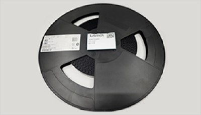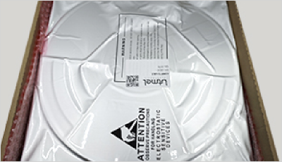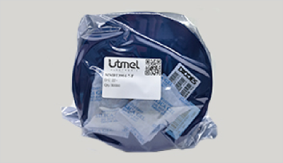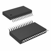

Texas Instruments TLV320AIC12KIDBTG4
30 Termination 0.5mm CODEC TLV320AIC12 30 Pin 1.8V 30-TFSOP (0.173, 4.40mm Width)
Manufacturer No:
TLV320AIC12KIDBTG4
Tiny WHSLManufacturer:
Utmel No:
2502-TLV320AIC12KIDBTG4
Package:
30-TFSOP (0.173, 4.40mm Width)
Description:
30 Termination 0.5mm CODEC TLV320AIC12 30 Pin 1.8V 30-TFSOP (0.173, 4.40mm Width)
Quantity:
Unit Price: $4.626816
Ext Price: $4.63
Delivery:


Payment:


In Stock : 200
Minimum: 1 Multiples: 1
Qty
Unit Price
Ext Price
1
$4.626816
$4.63
10
$4.364921
$43.65
100
$4.117850
$411.78
500
$3.884764
$1,942.38
1000
$3.664872
$3,664.87
Want a lower wholesale price? Please send RFQ, we will respond immediately.
RFQ Now
Add to RFQ list
You may place an order without registering to Utmel.
We strongly suggest you sign in before purchasing as you can track your order in real time.
For your convenience, we accept multiple payment methods in USD, including PayPal, Credit Card, and wire transfer.
RFQ (Request for Quotations)It is recommended to request for quotations to get the latest prices and inventories about the part.
Our sales will reply to your request by email within 24 hours.
1. You'll receive an order information email in your inbox. (Please remember to check the spam folder if you didn't hear from us).
2. Since inventories and prices may fluctuate to some extent, the sales manager is going to reconfirm the order and let you know if there are any updates.
- TypeParameter
- Lifecycle Status
Lifecycle Status refers to the current stage of an electronic component in its product life cycle, indicating whether it is active, obsolete, or transitioning between these states. An active status means the component is in production and available for purchase. An obsolete status indicates that the component is no longer being manufactured or supported, and manufacturers typically provide a limited time frame for support. Understanding the lifecycle status is crucial for design engineers to ensure continuity and reliability in their projects.
ACTIVE (Last Updated: 2 days ago) - Factory Lead Time6 Weeks
- Mounting Type
The "Mounting Type" in electronic components refers to the method used to attach or connect a component to a circuit board or other substrate, such as through-hole, surface-mount, or panel mount.
Surface Mount - Package / Case
refers to the protective housing that encases an electronic component, providing mechanical support, electrical connections, and thermal management.
30-TFSOP (0.173, 4.40mm Width) - Surface Mount
having leads that are designed to be soldered on the side of a circuit board that the body of the component is mounted on.
YES - Number of Pins30
- Weight97.49401mg
- Operating Temperature
The operating temperature is the range of ambient temperature within which a power supply, or any other electrical equipment, operate in. This ranges from a minimum operating temperature, to a peak or maximum operating temperature, outside which, the power supply may fail.
-40°C~85°C - Packaging
Semiconductor package is a carrier / shell used to contain and cover one or more semiconductor components or integrated circuits. The material of the shell can be metal, plastic, glass or ceramic.
Tube - JESD-609 Code
The "JESD-609 Code" in electronic components refers to a standardized marking code that indicates the lead-free solder composition and finish of electronic components for compliance with environmental regulations.
e4 - Pbfree Code
The "Pbfree Code" parameter in electronic components refers to the code or marking used to indicate that the component is lead-free. Lead (Pb) is a toxic substance that has been widely used in electronic components for many years, but due to environmental concerns, there has been a shift towards lead-free alternatives. The Pbfree Code helps manufacturers and users easily identify components that do not contain lead, ensuring compliance with regulations and promoting environmentally friendly practices. It is important to pay attention to the Pbfree Code when selecting electronic components to ensure they meet the necessary requirements for lead-free applications.
yes - Part Status
Parts can have many statuses as they progress through the configuration, analysis, review, and approval stages.
Active - Moisture Sensitivity Level (MSL)
Moisture Sensitivity Level (MSL) is a standardized rating that indicates the susceptibility of electronic components, particularly semiconductors, to moisture-induced damage during storage and the soldering process, defining the allowable exposure time to ambient conditions before they require special handling or baking to prevent failures
2 (1 Year) - Number of Terminations30
- ECCN Code
An ECCN (Export Control Classification Number) is an alphanumeric code used by the U.S. Bureau of Industry and Security to identify and categorize electronic components and other dual-use items that may require an export license based on their technical characteristics and potential for military use.
EAR99 - TypeVoice-Band
- Terminal Finish
Terminal Finish refers to the surface treatment applied to the terminals or leads of electronic components to enhance their performance and longevity. It can improve solderability, corrosion resistance, and overall reliability of the connection in electronic assemblies. Common finishes include nickel, gold, and tin, each possessing distinct properties suitable for various applications. The choice of terminal finish can significantly impact the durability and effectiveness of electronic devices.
Nickel/Palladium/Gold (Ni/Pd/Au) - Terminal Position
In electronic components, the term "Terminal Position" refers to the physical location of the connection points on the component where external electrical connections can be made. These connection points, known as terminals, are typically used to attach wires, leads, or other components to the main body of the electronic component. The terminal position is important for ensuring proper connectivity and functionality of the component within a circuit. It is often specified in technical datasheets or component specifications to help designers and engineers understand how to properly integrate the component into their circuit designs.
DUAL - Terminal Form
Occurring at or forming the end of a series, succession, or the like; closing; concluding.
GULL WING - Peak Reflow Temperature (Cel)
Peak Reflow Temperature (Cel) is a parameter that specifies the maximum temperature at which an electronic component can be exposed during the reflow soldering process. Reflow soldering is a common method used to attach electronic components to a circuit board. The Peak Reflow Temperature is crucial because it ensures that the component is not damaged or degraded during the soldering process. Exceeding the specified Peak Reflow Temperature can lead to issues such as component failure, reduced performance, or even permanent damage to the component. It is important for manufacturers and assemblers to adhere to the recommended Peak Reflow Temperature to ensure the reliability and functionality of the electronic components.
260 - Number of Functions1
- Supply Voltage
Supply voltage refers to the electrical potential difference provided to an electronic component or circuit. It is crucial for the proper operation of devices, as it powers their functions and determines performance characteristics. The supply voltage must be within specified limits to ensure reliability and prevent damage to components. Different electronic devices have specific supply voltage requirements, which can vary widely depending on their design and intended application.
1.8V - Terminal Pitch
The center distance from one pole to the next.
0.5mm - Base Part Number
The "Base Part Number" (BPN) in electronic components serves a similar purpose to the "Base Product Number." It refers to the primary identifier for a component that captures the essential characteristics shared by a group of similar components. The BPN provides a fundamental way to reference a family or series of components without specifying all the variations and specific details.
TLV320AIC12 - Pin Count
a count of all of the component leads (or pins)
30 - Interface
In electronic components, the term "Interface" refers to the point at which two different systems, devices, or components connect and interact with each other. It can involve physical connections such as ports, connectors, or cables, as well as communication protocols and standards that facilitate the exchange of data or signals between the connected entities. The interface serves as a bridge that enables seamless communication and interoperability between different parts of a system or between different systems altogether. Designing a reliable and efficient interface is crucial in ensuring proper functionality and performance of electronic components and systems.
2-Wire, I2C, Serial - Max Supply Voltage
In general, the absolute maximum common-mode voltage is VEE-0.3V and VCC+0.3V, but for products without a protection element at the VCC side, voltages up to the absolute maximum rated supply voltage (i.e. VEE+36V) can be supplied, regardless of supply voltage.
3.6V - Min Supply Voltage
The minimum supply voltage (V min ) is explored for sequential logic circuits by statistically simulating the impact of within-die process variations and gate-dielectric soft breakdown on data retention and hold time.
1.1V - Supply Current-Max
Supply Current-Max refers to the maximum amount of current that an electronic component or circuit can draw from its power supply under specified operating conditions. It is a critical parameter that determines the power consumption and thermal performance of the device. Exceeding this limit can lead to overheating, potential damage, or failure of the component. Knowing the Supply Current-Max helps in designing circuits that ensure proper operation and reliability.
2mA - Data Interface
A Data Interface in EDQ is a template of a set of attributes representing a given entity, used to create processes that read from, or write to, interfaces rather than directly from or to sources or targets of data.
Serial - Sampling Rate
often described in the context of signal processing as the number of samples per time.
104 ksps - Voltage - Supply, Analog
Voltage - Supply, Analog is a parameter in electronic components that specifies the range of voltage levels required to power the analog circuitry within the component. This parameter indicates the minimum and maximum voltage levels that the component can accept for proper operation of its analog functions. It is crucial to ensure that the voltage supplied to the component falls within this specified range to prevent damage and ensure optimal performance. Understanding and adhering to the "Voltage - Supply, Analog" parameter is essential for the proper functioning of analog circuits in electronic components.
2.7V~3.6V - Voltage - Supply, Digital
Voltage - Supply, Digital is a parameter that specifies the voltage level required to power the digital circuitry within an electronic component, such as an integrated circuit or a microcontroller. This parameter is crucial for ensuring proper operation of the digital components, as supplying the correct voltage level is essential for reliable performance. The specified voltage range typically includes both minimum and maximum values within which the component can operate safely and efficiently. It is important to adhere to the recommended voltage supply range to prevent damage to the component and to maintain the integrity of the digital signals being processed.
1.65V~1.95V - Power Consumption
Power consumption is the amount of input energy (measured in watts) required for an electrical appliance to function. This is opposed to power output which is a measure of the level of performance, of a heat pump for example.
11.2mW - Max Output Power
The maximum output power = the maximum output current × the rated output voltage
190mW - Analog Input Voltage-Max
Analog Input Voltage-Max refers to the maximum voltage level that can be safely applied to the input of an electronic component, such as an integrated circuit or sensor, without causing damage. This parameter is crucial for ensuring the proper functioning and longevity of the component. Exceeding the specified maximum input voltage can lead to overloading, overheating, or even permanent damage to the component. It is important for designers and engineers to carefully consider and adhere to this parameter when designing circuits or systems to prevent potential failures and ensure reliable operation.
2V - Signal to Noise Ratio (SNR)
Signal to Noise Ratio (SNR) is a measure used in electronics to quantify the ratio of the strength of a desired signal to the strength of background noise. It is commonly expressed in decibels (dB) and is used to evaluate the quality of a signal transmission or processing system. A higher SNR indicates a stronger, clearer signal relative to the background noise, resulting in better performance and accuracy in electronic components such as amplifiers, receivers, and communication systems. SNR is crucial in ensuring reliable and efficient operation of electronic devices by minimizing the impact of unwanted noise on the signal quality.
84 dB - Resolution (Bits)
Resolution (Bits) in electronic components refers to the number of bits used to represent the analog signal in digital form. It indicates the level of detail or precision with which the analog signal can be converted into digital data. A higher resolution means more bits are used, allowing for finer distinctions to be made between different signal levels. For example, an 8-bit resolution can represent 256 different levels, while a 16-bit resolution can represent 65,536 levels. In general, a higher resolution leads to better accuracy and fidelity in the digital representation of the original analog signal.
16 b - Number of DAC Channels
A DAC is a device that converts a digital, typically binary, code to an analog signal, such as a current, voltage, or electric charge. One DAC converter can have several channels. Each channel can sample an analog output from numerical values that are converted to output voltages.
1 - Number of Analog Inputs3
- Sigma Delta
In electronic components, "Sigma Delta" refers to a type of analog-to-digital converter (ADC) architecture commonly used in applications requiring high resolution and low noise. The Sigma Delta ADC works by oversampling the input signal at a much higher frequency than the desired output rate, and then using a digital filter to reduce the noise and quantization errors. This approach allows for achieving high resolution with relatively simple analog circuitry. The name "Sigma Delta" comes from the use of sigma (Σ) for the oversampling and delta (Δ) for the quantization error feedback mechanism. Overall, Sigma Delta ADCs are known for their ability to provide high-resolution conversion with low noise and are commonly used in audio, instrumentation, and sensor applications.
Yes - Number of ADCs / DACs1 / 1
- Filter
In electronic components, the parameter "Filter" refers to a device or circuit that is used to selectively allow certain frequencies to pass through while attenuating or blocking others. Filters are commonly used in electronic systems to remove unwanted noise or interference, shape the frequency response of a signal, or separate different signals in a multi-channel system.Filters can be categorized based on their frequency response characteristics, such as low-pass, high-pass, band-pass, and band-stop filters. Each type of filter has a specific cutoff frequency that determines the range of frequencies that are allowed to pass through. Filters can be implemented using various components such as resistors, capacitors, and inductors, or using digital signal processing techniques in software.Overall, filters play a crucial role in signal processing and communication systems by helping to improve signal quality, reduce interference, and enhance the performance of electronic devices.
YES - Dynamic Range, ADCs / DACs (db) Typ
The parameter "Dynamic Range, ADCs / DACs (db) Typ" in electronic components refers to the range of signal amplitudes that can be accurately measured or reproduced by an analog-to-digital converter (ADC) or digital-to-analog converter (DAC). It is typically expressed in decibels (dB) and represents the ratio between the largest and smallest signals that can be effectively processed by the ADC or DAC without distortion or loss of accuracy. A higher dynamic range indicates a greater ability to capture or reproduce a wide range of signal amplitudes, making the component more versatile and suitable for applications requiring precise signal processing. It is an important specification to consider when selecting ADCs or DACs for audio, video, communications, and other high-fidelity applications.
85 / 92 - Output Code
An output code is an integer representation of binary bits.
TWOS COMPLEMENT - S/N Ratio, ADCs / DACs (db) Typ
The parameter "S/N Ratio, ADCs / DACs (db) Typ" in electronic components refers to the Signal-to-Noise Ratio of Analog-to-Digital Converters (ADCs) and Digital-to-Analog Converters (DACs). It represents the ratio of the desired signal level to the background noise level, typically measured in decibels (dB). A higher S/N ratio indicates better performance in terms of signal clarity and accuracy, as it signifies that the signal is stronger relative to any unwanted noise present in the system. This parameter is crucial in determining the quality and fidelity of analog-to-digital and digital-to-analog conversion processes in electronic devices.
84 / 92 - Input Code
Input Code is a parameter used in electronic components to specify the code or signal that is received by the component as input. This code is typically used to control or configure the behavior of the component, such as setting operating modes or selecting specific functions. The input code can be in various forms, such as binary, hexadecimal, or alphanumeric, depending on the component and its application. It is important to correctly provide the input code to ensure proper operation and functionality of the electronic component.
TWOS COMPLEMENT - Height1.2mm
- Length7.8mm
- Width4.4mm
- Thickness
Thickness in electronic components refers to the measurement of how thick a particular material or layer is within the component structure. It can pertain to various aspects, such as the thickness of a substrate, a dielectric layer, or conductive traces. This parameter is crucial as it impacts the electrical, mechanical, and thermal properties of the component, influencing its performance and reliability in electronic circuits.
1mm - Radiation Hardening
Radiation hardening is the process of making electronic components and circuits resistant to damage or malfunction caused by high levels of ionizing radiation, especially for environments in outer space (especially beyond the low Earth orbit), around nuclear reactors and particle accelerators, or during nuclear accidents or nuclear warfare.
No - RoHS Status
RoHS means “Restriction of Certain Hazardous Substances” in the “Hazardous Substances Directive” in electrical and electronic equipment.
ROHS3 Compliant - Lead Free
Lead Free is a term used to describe electronic components that do not contain lead as part of their composition. Lead is a toxic material that can have harmful effects on human health and the environment, so the electronics industry has been moving towards lead-free components to reduce these risks. Lead-free components are typically made using alternative materials such as silver, copper, and tin. Manufacturers must comply with regulations such as the Restriction of Hazardous Substances (RoHS) directive to ensure that their products are lead-free and environmentally friendly.
Lead Free
![TLV320AIC3254IRHBR]()
TLV320AIC3254IRHBR
Texas Instruments![TLV320AIC3204IRHBT]()
TLV320AIC3204IRHBT
Texas Instruments![TLC320AC01CFN]()
TLC320AC01CFN
Texas Instruments![TLV320AIC3204IRHBR]()
TLV320AIC3204IRHBR
Texas Instruments![TLV320AIC3100IRHBR]()
TLV320AIC3100IRHBR
Texas Instruments![TLV320AIC3106IRGZR]()
TLV320AIC3106IRGZR
Texas Instruments![TLV320AIC3104IRHBT]()
TLV320AIC3104IRHBT
Texas Instruments![PCM3001E]()
PCM3001E
Texas Instruments![TLV320AIC10IPFB]()
TLV320AIC10IPFB
Texas Instruments![TLV320AIC3105IRHBR]()
TLV320AIC3105IRHBR
Texas Instruments


