Battery Charger IC Guide

Understanding Battery Charger IC Specifications
Catalog |
I The principle of battery charger IC to identify battery insertion |
III How to solve the power consumption problem of battery charger IC? |
I The principle of battery charger IC to identify battery insertion
Many existing battery charging solutions use charge management ICs, which can realize charge current regulation, charge voltage protection, etc. Among them, identifying whether the battery is inserted or not is also one of the basic functions.
For a removable battery product, it is also an important issue to identify whether the battery is inserted or not, so TI's BQ24125 battery charger IC is used as an example to analyze whether the battery is inserted or not.
The following is the logic diagram for the BQ24125 to detect the battery.

Logic diagram of BQ24125 detecting battery
When the voltage on the pins connected to the battery charger IC drops, the reason for the drop is mainly because the battery is discharged with load or the battery is pulled out. When the battery voltage drops to the voltage point for re-charging, the battery charger IC first detects whether the battery is inserted or not, and enters the battery detection logic, and then re-charges.
Enabling detection current I_DETECT=400uA, enabling duration period t_DETECT=1s, in order to let the battery input current to the internal IC. during the enabling period to detect whether the battery pin voltage is greater than V_SHORT, V_SHORT is defined in BQ24125 as follows.

When identifying V_BAT>V_SHORT, it means that the battery is inserted normally and can enter the charging logic judgment, if V_BAT<V_SHORT, it means that the voltage exceeds the minimum voltage that should exist when the battery is inserted, then it enters the next round of judgment.
When V_BAT<V_SHORT, another wake-up current I_WAKE=2mA is enabled, and the duration period of the enable is t_WAKE=0.5s. The wake-up current is to output the charging current to the battery end. The purpose is to avoid the battery over-discharge protection shutdown output resulting in the voltage drop at the battery end. At this time, if no external battery is identified, the output voltage is V_OVP, and V_OVP is defined as follows.

V_OVP is the charging overvoltage protection voltage at the battery end. When the point is exceeded, it will trigger the battery charger IC to over-voltage protection. Therefore, if the battery is not inserted, the voltage at the battery end during t_WAKE will be V_OVP, and the battery detection will enter the start cycle detection and start the cycle again from ①. If there is a battery, the battery will recover from the over-discharge protection state, and the voltage will drop to the battery voltage, then the battery will be judged to be present and enter the charging logic.
In view of the above analysis, it can be known that when the battery is not inserted, the voltage at the battery detection end will jump between 0 and V_OVP. When the battery is inserted at the time of detection, it will i.e. resume to the battery voltage, as follows.
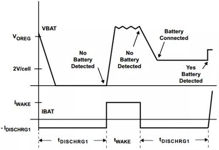
battery voltage graph
II What should a good battery charger IC be like?
Safety. As a power product use safety is still very important, after all, the charger explosion is possible. So choose the 3C certification battery charger IC. There are generally no safety problems.
Power. For battery charger IC power selection, it depends on how much power you need on your side.
Compatibility. The battery charger IC should not only charge fast but also charge widely. Since it is necessary to charge a wide range, it is necessary to take into account the issue of compatibility.
Small size. battery charger IC is still used for charging. Considering its practicality, do not require a lot, but should be easy to carry.
Cost. As a good battery charger IC, the cost performance must also be taken into account. The higher the power, the higher the price of the charger IC.
Recommended battery charger ICs
BQ2057TSN Texas Instruments
MCP73844-820I/MS Microchip Technology
UC3906N Texas Instruments
III How to solve the power consumption problem of battery charger IC?
To form the simplest understanding of battery charger IC in your mind, it is most accurate to think of it as a voltage regulator with an adjustable current limiting function. As a voltage regulator, its output voltage is determined by itself, but whether the voltage at its output can be stabilized at the point determined by itself depends on the balance between its current output and load consumption. When the current output capacity is lower than the load consumption capacity, the actual output voltage is determined by the load, for the battery charger IC. the output voltage at this time is the battery voltage. Only when the battery voltage gradually rises to the output voltage set by the regulator, the battery's ability to draw current gradually decreases, and once the balance between the drawing capacity and output capacity is crossed, the battery draws less and less current, and the output voltage is stabilized at the pre-set point, which is the so-called constant voltage charging state.
In order to comply with the characteristics of Li-ion batteries, the battery charger IC charges the battery at a very low current when the battery voltage is below the pre-charge threshold (approximately 3V). After this threshold is exceeded, charging starts at a high current so that the battery can be fully charged as soon as possible.
The supply voltage into the charging port is usually 5V (nominal). Assuming a charging current of 1A, we can immediately calculate that the maximum power consumption on the linear battery charger IC will be (5V-3V)x1A=2W. Even if the battery voltage has risen to 4.2V, the battery charger IC will consume up to (5V-4.2V)x1A=0.8W. For these reasons The battery charger IC will consume as much as (5V-4.2V)x1A=0.8W. Due to these reasons, plus the limitation of heat dissipation, it is normal to feel hot when charging the phone.
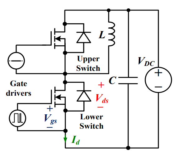
To solve the heat problem of linear battery charger ICs, it is inevitable to introduce battery charger ICs that work in a switching mode. Another newer approach is direct charging. which eliminates the voltage conversion link. Since the vast majority of usage environments are where the input voltage is higher than the battery voltage, the switching mode battery charger IC with Buck architecture has become the mainstream of the market with the circuit architecture shown in the figure below.
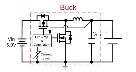
Buck Circuit Architecture
In essence, it is a Buck regulator with an adjustable current limiting function. However, compared with the common Buck converter and linear battery charger IC. the Buck mode battery charger IC is much more complex.
The Buck circuit has the effect of current amplification, and its output current is higher than the input current. This has the advantage of higher efficiency, lower heat generation, and faster charging. but because the input and output currents are not equal, it is not possible to know the input and output currents by measuring only the current at one place on the output, as in the case of a linear battery charger IC. which must measure both the output and input currents. Only after doing so, the battery charger IC can bring down the input current when the input current exceeds a certain limit so that it does not exceed the limit.
Some external power supplies do not have sufficient power supply capacity, and when the load is heavy, the output voltage will drop. If the battery charger IC does not take this into account and only focuses on meeting the output current needs, the external power supply will be dragged down, so the battery charger IC also needs to monitor the input voltage and reduce the input current demand when the input voltage is below a certain threshold to ensure that the system can still work properly.
The ability to limit the input current to a certain maximum value is called dynamic input current regulation or average input current regulation, and the ability to control the minimum input voltage to a certain threshold is called minimum input voltage regulation. Both of these capabilities are used to protect the input power supply, which is not needed by the battery charger IC itself, but ensures that the system does not go wrong, and is therefore a brand new battery charger IC design must be considered. Engineers should look at this as a priority when selecting a model.
As the Buck can be bucked with high efficiency, the input voltage can be higher, which has the advantage that the input current can be smaller at the same input power, which reduces the requirement for the overcurrent capability of the connected devices, making it possible to transfer more power under the same conditions to meet the needs of fast charging systems. To increase the input voltage it is necessary to improve the voltage withstand capability of the device, which requires the use of a new high-voltage process.
The RT9451, for example, has a maximum operating voltage of 12V (withstands 28V shock) and a charging current of up to 4A, which means it can charge batteries at a very high speed. Due to the increasing number of adjustable parameters, such battery charger ICs are designed to be intelligent, allowing the user to adjust all parameters and control the working process via the I2C interface, while the application design is still very simple from the hardware point of view.
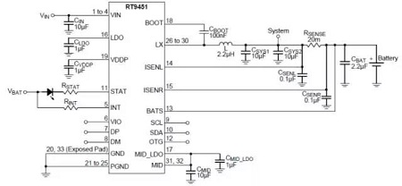
RT9451 application circuit diagram
The RT9451's charging voltage can be adjusted from 3.5V to 4.44V, so it can be used to charge ordinary Li-ion batteries, and it is also feasible to charge Li-iron phosphate ion batteries, so it can be used in a wide range of applications.
Readers who are concerned about the circuit architecture can refocus on the circuit structure of the Buck battery charger IC and you will find that it can be used as a Boost converter, only the direction of its energy transfer has changed.
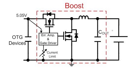
Buck charging IC circuit structure
Now, the original battery becomes the power provider, and the original input becomes the output, which can be powered by simply connecting to the load, and this is exactly how USB OTG applications require it to be. When used in this way, the components in the circuit do not change, only the operating mode of the battery charger IC changes. The minimum current limit of the switching tube is 4A, ensuring a load capacity of 1.6A or more is not a problem, and thus can meet the needs of many applications.
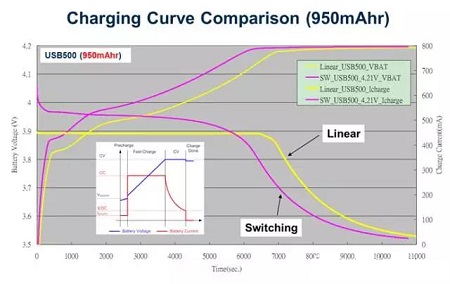
What are the specific benefits of a battery charger IC for Li-ion batteries that operates in a switching mode compared to a linear charging mode? Take a look at the following comparison chart.
charging curve comparison
Also using the linear battery charger IC and switch mode, the battery charger IC charges a 950mAh Li-ion battery in USB 500mA input current limit mode. The switching mode battery charger IC can charge at a maximum of 600mA, and the charging time from the battery voltage of 3.5V to the start of constant voltage mode is much shorter, thus allowing the battery to be filled up faster, and the heat generated during the charging process will, of course, be much less.
1.What is a battery charger IC?
Battery charger ICs are integrated circuits (IC) that are used to charge batteries. Switching chargers use an inductor, transformer, or capacitor to transfer energy from the input to the battery in discrete packets. Some battery charger ICs are designed to charge lithium (Li) ion or lead acid batteries.
2.What is battery charger circuit?
It is a simple method that uses a small constant current to charge the battery during the complete charging process. When the battery reaches its predefined value, CC charging stops. Mostly, this method is used for charging NiCd, NiMH and Li-ion batteries.
3.What is the battery charger IC mainly responsible for?
Converting AC power into DC power to match the devices.
4.What do many existing battery charging solutions use?
Charge management ICs
5.What is one of the basic functions of a battery charging solution?
Identifying whether the battery is inserted or not.
 Discovering New and Advanced Methodology for Determining the Dynamic Characterization of Wide Bandgap DevicesSaumitra Jagdale15 March 20242449
For a long era, silicon has stood out as the primary material for fabricating electronic devices due to its affordability, moderate efficiency, and performance capabilities. Despite its widespread use, silicon faces several limitations that render it unsuitable for applications involving high power and elevated temperatures. As technological advancements continue and the industry demands enhanced efficiency from devices, these limitations become increasingly vivid. In the quest for electronic devices that are more potent, efficient, and compact, wide bandgap materials are emerging as a dominant player. Their superiority over silicon in crucial aspects such as efficiency, higher junction temperatures, power density, thinner drift regions, and faster switching speeds positions them as the preferred materials for the future of power electronics.
Read More A Comprehensive Guide to FPGA Development BoardsUTMEL11 September 202513859
This comprehensive guide will take you on a journey through the fascinating world of FPGA development boards. We’ll explore what they are, how they differ from microcontrollers, and most importantly, how to choose the perfect board for your needs. Whether you’re a seasoned engineer or a curious hobbyist, prepare to unlock new possibilities in hardware design and accelerate your projects. We’ll cover everything from budget-friendly options to specialized boards for image processing, delve into popular learning paths, and even provide insights into essential software like Vivado. By the end of this article, you’ll have a clear roadmap to navigate the FPGA landscape and make informed decisions for your next groundbreaking endeavor.
Read More Applications of FPGAs in Artificial Intelligence: A Comprehensive GuideUTMEL29 August 20253433
This comprehensive guide explores FPGAs as powerful AI accelerators that offer distinct advantages over traditional GPUs and CPUs. FPGAs provide reconfigurable hardware that can be customized for specific AI workloads, delivering superior energy efficiency, ultra-low latency, and deterministic performance—particularly valuable for edge AI applications. While GPUs excel at parallel processing for training, FPGAs shine in inference tasks through their adaptability and power optimization. The document covers practical implementation challenges, including development complexity and resource constraints, while highlighting solutions like High-Level Synthesis tools and vendor-specific AI development suites from Intel and AMD/Xilinx. Real-world applications span telecommunications, healthcare, autonomous vehicles, and financial services, demonstrating FPGAs' versatility in mission-critical systems requiring real-time processing and minimal power consumption.
Read More 800G Optical Transceivers: The Guide for AI Data CentersUTMEL24 December 20253401
The complete guide to 800G Optical Transceiver standards (QSFP-DD vs. OSFP). Overcome supply shortages and scale your AI data center with Utmel Electronic.
Read More Xilinx FPGAs: From Getting Started to Advanced Application DevelopmentUTMEL09 September 20254172
This guide is your comprehensive roadmap to understanding and mastering the world of Xilinx FPGA technology. From selecting your first board to deploying advanced AI applications, we'll cover everything you need to know to unlock the potential of these remarkable devices. The global FPGA market is on a significant growth trajectory, expected to expand from USD 8.37 billion in 2025 to USD 17.53 billion by 2035. This surge is fueled by the relentless demand for high-performance, adaptable computing in everything from 5G networks and data centers to autonomous vehicles and the Internet of Things (IoT). This guide will walk you through the key concepts, tools, and products in the Xilinx ecosystem, ensuring you're well-equipped to be a part of this technological revolution.
Read More
Subscribe to Utmel !
![AT88SC6416C-MJTG]() AT88SC6416C-MJTG
AT88SC6416C-MJTGMicrochip Technology
![HCS512T-I/SO]() HCS512T-I/SO
HCS512T-I/SOMicrochip Technology
![LZ9FC23]() LZ9FC23
LZ9FC23Sharp Microelectronics
![HCS370/ST]() HCS370/ST
HCS370/STMicrochip Technology
![SI8261BCD-C-IS]() SI8261BCD-C-IS
SI8261BCD-C-ISSilicon Labs
![SI8233BB-D-IS]() SI8233BB-D-IS
SI8233BB-D-ISSilicon Labs
![ACNW3190-000E]() ACNW3190-000E
ACNW3190-000EBroadcom Limited
![MCS3142-I/ST]() MCS3142-I/ST
MCS3142-I/STMicrochip Technology
![AT88SC3216C-SU]() AT88SC3216C-SU
AT88SC3216C-SUMicrochip Technology
![FOD8321V]() FOD8321V
FOD8321VON Semiconductor


 Product
 Brand
Brand Articles
 Tools
Tools


