Product
 Brand
Brand Articles
 Tools
ToolsWide Band Differential Amplifier Calculator Overview
The Wide Band Differential Amplifier Calculator helps estimate the main operating values of a wide-band differential amplifier, including differential gain, input and output voltage relationships, bias current, load effects, and frequency-response related terms. It is useful for early-stage circuit design when you need a quick check before selecting devices, resistor values, supply rails, and layout constraints.
A wide-band differential amplifier amplifies the difference between two input signals while rejecting the signal that is common to both inputs. This makes it valuable in high-speed signal chains, ADC driver circuits, communication receivers, balanced audio paths, sensor interfaces, and other applications where noise rejection and bandwidth are both important.
What Is a Wide Band Differential Amplifier?
A differential amplifier has two input terminals and responds mainly to the voltage difference between them. If the same voltage appears on both inputs, an ideal differential amplifier rejects it. In real circuits, the amount of rejection depends on resistor matching, device matching, circuit topology, layout symmetry, and the amplifier's common-mode rejection ratio.
A wide-band amplifier is designed to maintain useful gain over a broad frequency range. In a differential design, bandwidth must be considered together with gain, input capacitance, load capacitance, parasitic inductance, feedback stability, resistor tolerance, and the common-mode input and output ranges.
What This Calculator Can Help You Estimate
| Result | Meaning | Design Use |
|---|---|---|
| Differential input voltage | The voltage difference between the two input nodes. | Checks the signal level that the amplifier actually amplifies. |
| Differential gain | The gain applied to the differential input signal. | Helps determine expected output amplitude and required resistor ratios. |
| Common-mode voltage | The average voltage shared by the two input nodes. | Checks whether the input stays inside the amplifier's common-mode range. |
| Bias or tail current | The current that sets the operating point of a transistor differential pair. | Helps set transconductance, output swing, linearity, and power dissipation. |
| Frequency response | The way gain changes as signal frequency increases. | Helps judge whether the circuit has enough bandwidth for the target signal. |
Common Input Parameters
| Input | What It Represents | Typical Unit |
|---|---|---|
| V1, V2 | The two input voltages applied to the differential amplifier. | V |
| VCC, VEE | The positive and negative supply rails, or the single-supply operating limits. | V |
| R1, R2, R3, R4 | Gain-setting or load resistors, depending on the amplifier topology. | Ω or kΩ |
| Load resistance | The resistance connected to the amplifier output. | Ω or kΩ |
| Bias current | The operating current used by a transistor pair or active load. | mA or µA |
| Bandwidth or frequency | The frequency range where the calculated gain should remain valid. | Hz, kHz, MHz |
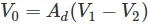
Core Differential Amplifier Formulas
The basic differential input voltage is:
Vdiff = V1 - V2
The common-mode input voltage is:
Vcm = (V1 + V2) / 2
For a voltage-gain model, the ideal output is:
Vout = Ad × (V1 - V2)
where Ad is the differential gain. If the circuit is an op-amp difference amplifier and the resistor ratios are matched, the commonly used relationship is:
Vout = (R2 / R1) × (V2 - V1), when R2 / R1 = R4 / R3.
Common-mode rejection ratio is often written as:
CMRR = Ad / Acm
and in decibels:
CMRR(dB) = 20 log10(Ad / Acm)
Example Calculation
Assume the two input voltages are V1 = 1.20 V and V2 = 1.10 V, and the differential gain is Ad = 20 V/V.
Vdiff = 1.20 V - 1.10 V = 0.10 V
Vout = 20 × 0.10 V = 2.0 V
This simple result assumes the amplifier has enough output swing, the input common-mode voltage is within range, and the target signal frequency is inside the usable bandwidth of the circuit.
Wideband Design Considerations
| Design Factor | Why It Matters |
|---|---|
| Gain-bandwidth tradeoff | Higher gain usually reduces available closed-loop bandwidth unless the selected amplifier has enough speed margin. |
| Resistor matching | Mismatch in resistor ratios reduces common-mode rejection and turns common-mode voltage into output error. |
| Input and output common-mode range | The circuit may calculate correctly but still clip or distort if the common-mode voltage is outside the valid range. |
| Parasitic capacitance | PCB capacitance, probe capacitance, and package capacitance can reduce bandwidth or cause peaking. |
| Layout symmetry | Balanced routing improves phase matching, noise rejection, and high-frequency performance. |
| Termination and load | High-speed differential outputs often need controlled impedance and proper termination. |
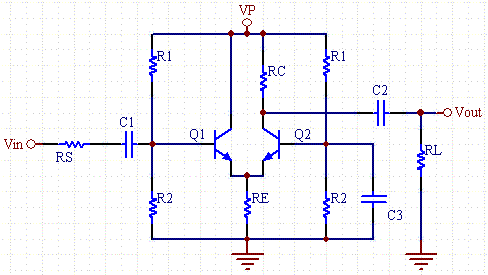
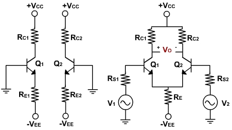
Differential Amplifier Circuit
Differential amplifiers can be built with BJTs, MOSFETs, op amps, or fully differential amplifier ICs. The same core idea applies: the circuit amplifies the difference between two inputs and tries to reject the common signal shared by both inputs.
Types of Differential Amplifiers
BJT Differential Amplifier
A BJT differential pair uses two matched transistors and a shared emitter current source. It is widely used in analog IC input stages because it can provide good gain and predictable small-signal behavior when the devices are well matched.

MOSFET Differential Amplifier
A MOSFET differential pair uses matched field-effect transistors. It is common in CMOS analog design and is useful when high input impedance is required. Its performance depends strongly on bias current, overdrive voltage, device matching, and layout.
Op-Amp Difference Amplifier
An op-amp difference amplifier uses external resistors to set gain. For good common-mode rejection, the resistor ratios must be closely matched. Precision resistor networks or integrated difference-amplifier ICs are often preferred when high CMRR is required.
Fully Differential Amplifier
A fully differential amplifier produces two output signals that move in opposite directions around a defined output common-mode voltage. This topology is often used to drive high-speed ADCs because it can improve noise immunity and dynamic range when designed correctly.
How to Use the Calculator
Enter the input voltages, supply rails, resistor values, load conditions, bias values, and frequency-related parameters required by the calculator. After calculation, compare the output values with the selected amplifier or transistor datasheet. Pay special attention to maximum output swing, input common-mode range, bandwidth, slew rate, power dissipation, and thermal limits.
For wideband circuits, the calculator should be treated as a first-pass design aid. Final designs should be verified with the device datasheet, manufacturer simulation model, PCB layout review, and bench measurement.
How to Read the Results
| Result Check | Good Sign | Warning Sign |
|---|---|---|
| Output voltage | The output is comfortably inside the supply rails. | The output is close to clipping or exceeds the allowed swing. |
| Common-mode voltage | The input and output common-mode levels match the device limits. | The common-mode level is outside the datasheet range. |
| Bandwidth | The usable bandwidth is higher than the highest signal frequency. | The circuit is near the bandwidth limit or shows gain peaking. |
| CMRR | The circuit rejects common-mode noise with enough margin. | Resistor mismatch or layout imbalance creates output error. |
Common Mistakes to Avoid
Do not assume that differential gain alone proves the design is valid. A circuit can have the correct calculated gain but still fail because of insufficient bandwidth, limited slew rate, output swing limits, unstable feedback, poor resistor matching, or unsuitable PCB layout.
Also avoid using loose-tolerance resistors in high-CMRR difference amplifier circuits. Even when all resistor values look close in absolute value, the ratio matching is what determines common-mode rejection.
Applications of Wide Band Differential Amplifiers
| Application | Why Differential Amplification Helps |
|---|---|
| ADC driver circuits | Converts or conditions signals for differential ADC inputs and helps control output common-mode voltage. |
| Communication receivers | Improves rejection of common noise picked up by balanced signal paths. |
| Sensor interfaces | Amplifies small differential sensor signals while reducing shared interference. |
| Balanced audio and video | Preserves signal integrity over cables and rejects external noise. |
| Current sensing | Measures small voltage drops across sense resistors in the presence of larger common-mode voltages. |
FAQ
Is a differential amplifier the same as an instrumentation amplifier?
No. An instrumentation amplifier is a precision amplifier architecture designed for high input impedance and high common-mode rejection. It uses differential amplification internally, but it is not the same as a simple difference amplifier.
Why does resistor matching affect CMRR?
In an op-amp difference amplifier, common-mode rejection depends on matched resistor ratios. If the ratios are not equal, some common-mode voltage appears as an output error.
Why is layout important in a wideband differential circuit?
At high frequency, trace length, parasitic capacitance, return paths, and impedance imbalance can change gain and phase. Symmetrical routing and short feedback paths help preserve bandwidth and noise rejection.
Can this calculator replace simulation?
No. The calculator is useful for quick design estimates, but final wideband designs should be checked with datasheets, SPICE or vendor simulation models, PCB layout review, and real measurements.
Related Online Calculation Tools
Op-Amp Voltage and Gain Calculator - calculates output voltage, inverting gain, and non-inverting gain for operational amplifier circuits.
Inverting Op-Amp Resistor Calculator - helps calculate resistor values for inverting operational amplifier circuits.
Comparator Hysteresis Calculator - calculates comparator threshold and hysteresis values.
Ohm's Law Calculator - calculates voltage, current, resistance, and power.
Voltage Divider Calculator - calculates output voltage and resistor values for voltage divider circuits.
Parallel and Series Resistor Calculator - calculates equivalent resistance for series and parallel resistor networks.