
 Product
 Brand
Brand Articles
 Tools
Tools
FPGA vs ASIC: Comprehensive Comparison Guide
Table of Contents
Introduction: The Hardware Dilemma
In the rapidly evolving world of electronic systems and digital design, choosing the right hardware implementation platform is a critical decision that can significantly impact project success. Engineers and project managers often find themselves at a crossroads between two powerful technologies: Field-Programmable Gate Arrays (FPGAs) and Application-Specific Integrated Circuits (ASICs).
This decision isn't merely a technical one—it affects development timelines, production costs, performance capabilities, and even long-term product viability. According to recent industry reports, the global FPGA market is projected to reach $13.2 billion by 2026, while the ASIC market is expected to grow to $32.12 billion by 2032, highlighting the significant role both technologies play in modern electronics.
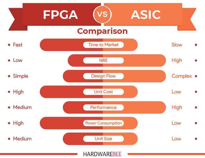
Visual representation of key differences between FPGA and ASIC technologies
"Selecting between FPGA and ASIC is one of the most consequential decisions in hardware development. It's not about which technology is better in absolute terms, but rather which one better suits your specific project requirements, timeline, and budget constraints."
— Dr. James Chen, Senior Hardware Architect at Silicon Innovations
Whether you're designing for telecommunications infrastructure, automotive systems, consumer electronics, industrial automation, or cutting-edge AI applications, this comprehensive guide will help you navigate the FPGA vs ASIC landscape with confidence. We'll examine their fundamental differences, analyze key performance metrics, explore cost considerations, and provide practical guidance to help you make an informed decision for your next project.
Key Question to Consider:
Are you prioritizing development speed and flexibility, or is manufacturing cost at scale your primary concern? Your answer may significantly influence your hardware choice.
Understanding the Basics: FPGA and ASIC Defined
Field-Programmable Gate Array (FPGA)
An FPGA is an integrated circuit designed to be configured by the customer or designer after manufacturing—hence the term "field-programmable." It consists of an array of programmable logic blocks and a hierarchy of reconfigurable interconnects that allow the blocks to be wired together.
FPGAs can implement any logical function that an ASIC could perform, but their ability to update functionality after shipping, partial reconfiguration, and low non-recurring engineering costs (NRE) offer advantages for many applications.
Configurable logic blocks (CLBs)
Programmable interconnects
I/O blocks for external connections
Memory resources (Block RAM)
DSP slices for mathematical operations
Application-Specific Integrated Circuits (ASIC)
An ASIC is an integrated circuit custom-designed for a specific application or purpose. Unlike FPGAs, once manufactured, an ASIC cannot be modified—its function is permanently set during the fabrication process.
ASICs are optimized for particular tasks and typically offer better performance, lower power consumption, and lower per-unit cost in high-volume production compared to FPGAs.
Custom-designed logic circuits
Fixed interconnect architecture
Optimized I/O interfaces
Dedicated memory structures
Custom processing units
Core Architectural Differences
The fundamental difference between FPGAs and ASICs lies in their architecture and design approach:
FPGAs contain pre-fabricated logic blocks and programmable routing resources that can be configured to implement custom logic functions. This programmability comes at the cost of additional circuitry overhead.
ASICs are built from the ground up for specific functions, with custom-designed transistor layouts optimized for their intended application. They lack programmable elements, making them more efficient but inflexible.
Video: Overview of ASIC and FPGA technologies and their advantages
Design and Development: Process Comparison
The development workflows for FPGAs and ASICs differ significantly, with major implications for project timelines, resource requirements, and risk profiles.

FPGA vs ASIC design flow comparison
FPGA Development Process
Design Entry: Create design using Hardware Description Languages (HDL) like VHDL or Verilog, or through schematic capture or high-level synthesis tools.
Functional Simulation: Verify logical correctness of the design through behavioral simulation.
Synthesis: Convert HDL code into a netlist of FPGA primitives.
Implementation: Place and route the design onto the FPGA fabric.
Timing Analysis: Ensure the design meets timing requirements.
Bitstream Generation: Create a configuration file.
Programming: Load the bitstream onto the FPGA.
Hardware Verification: Test functionality in actual hardware.
The FPGA development cycle enables rapid iteration and design changes. Engineers can reprogram devices in minutes, allowing quick debugging and feature updates without additional manufacturing costs.
ASIC Development Process
Specification: Define detailed requirements and specifications.
Architecture Design: Create high-level architecture based on specifications.
RTL Design: Develop hardware description using HDL.
Functional Verification: Verify design correctness through extensive simulation.
Logic Synthesis: Convert HDL to gate-level representation.
Physical Design: Convert logical design to physical layout, including floor planning, placement, and routing.
Verification: Perform physical verification, timing analysis, and power analysis.
Mask Generation: Create photomasks for fabrication.
Fabrication: Manufacture silicon wafers at foundry.
Testing and Packaging: Test fabricated chips and package them.
ASIC development requires significant upfront investment and typically takes 6-18 months from concept to silicon. Any design changes after fabrication necessitate a new production run, making errors extremely costly.
Thought-Provoking Question:
How might the ability to make post-deployment changes to your hardware affect your product's competitive advantage in a rapidly evolving market?
Development Tools and Ecosystem
Both FPGA and ASIC development rely on specialized tools and ecosystems:
| Aspect | FPGA | ASIC |
|---|---|---|
| Primary Tools | Vendor-specific IDEs (Xilinx Vivado, Intel Quartus Prime, Lattice Radiant) | Various EDA tools (Synopsys, Cadence, Mentor Graphics) |
| IP Ecosystem | Rich selection of pre-verified IP cores from vendors and third parties | Extensive IP marketplace, but integration requires more verification |
| Learning Curve | Moderate to steep, but more accessible for beginners | Very steep, requires specialized knowledge |
| Community Support | Active online communities, vendor forums, and resources | More specialized and often company-internal |
| Verification Tools | Integrated simulators, basic verification methodology | Advanced verification methodologies (UVM), formal verification |
The development environment choice has significant implications for team expertise requirements and project management. FPGA projects can often be executed with smaller teams, while ASIC projects typically require specialized expertise in various domains.
Performance Comparison: FPGA vs ASIC
When comparing FPGA and ASIC performance, several key metrics must be considered: processing speed, power consumption, physical size, and reliability.

Performance comparison between FPGA and ASIC across key metrics
Processing Speed and Performance
ASICs generally offer superior performance compared to FPGAs implementing the same function:
Clock Frequency: ASICs can typically operate at 3-4x higher clock frequencies than FPGAs due to optimized signal paths and reduced routing delays.
Latency: ASIC designs typically have lower latency for the same functions compared to FPGAs.
Throughput: ASICs can achieve higher data throughput, making them preferred for high-performance applications like network switches or cryptocurrency mining.
According to industry benchmarks, an ASIC implementation can run approximately 5-10 times faster than an equivalent FPGA design. For example, a 100MHz design on an FPGA might operate at 500MHz on an ASIC in the same process technology.
Power Efficiency
Power consumption is a critical consideration for many applications, particularly in mobile or battery-operated devices:
Static Power: FPGAs consume significant static power due to their programmable interconnects and configuration memory. ASICs optimize away unnecessary circuits, reducing leakage current.
Dynamic Power: ASICs typically require 5-10x less dynamic power than equivalent FPGA implementations due to optimized switching activity and reduced capacitive loads.
Power Management: Modern FPGAs include advanced power management features, but ASICs still maintain a significant efficiency advantage.
"In our datacenter AI acceleration project, replacing FPGA-based accelerators with custom ASICs reduced power consumption by 87% while increasing performance by 3.5x. The energy efficiency improvement was transformative for our operating costs."
— Maria Rodriguez, Chief Technology Officer at DataAI Solutions
Physical Size and Integration
The silicon area required for implementation impacts both cost and integration possibilities:
Silicon Area: ASIC implementations typically require 10-20x less silicon area than equivalent FPGA designs, allowing for smaller package sizes or integration of more functionality.
System-on-Chip Integration: ASICs can more easily integrate analog components, specialized I/O, and other system elements that might require external components with FPGAs.
Packaging: ASICs offer more flexibility in packaging options, potentially enabling smaller form factors.
Reliability and Security
Both technologies have different reliability and security characteristics:
SEU Sensitivity: FPGAs can be more susceptible to Single Event Upsets (SEUs) in high-radiation environments due to configuration memory.
Design Maturity: ASICs undergo more rigorous verification, potentially resulting in fewer functional bugs in production.
Security: FPGAs can be vulnerable to bitstream interception or reverse engineering, while ASICs can implement security features at the hardware level more efficiently.
Obsolescence: FPGAs can be reprogrammed to address security vulnerabilities discovered after deployment.
Thought-Provoking Question:
Given the performance advantages of ASICs, what specific application requirements might still make FPGAs the better choice despite their performance limitations?
Cost Analysis: Breaking Down the Economics
Cost considerations often play a decisive role in choosing between FPGA and ASIC implementations. The economic analysis must account for both non-recurring engineering (NRE) costs and recurring production costs.
Non-Recurring Engineering (NRE) Costs
NRE costs represent the one-time expenses required to design and prepare for production:
| Cost Category | FPGA | ASIC |
|---|---|---|
| Design & Development | $10K - $300K | $500K - $5M+ |
| EDA Tools & Software | $5K - $100K per year | $500K - $2M+ per year |
| IP Licensing | $0 - $100K | $50K - $2M+ |
| Verification | $10K - $200K | $500K - $3M+ |
| Mask Sets & Fabrication Setup | $0 (uses existing FPGA) | $500K - $5M+ (depends on process node) |
| Total NRE | $25K - $600K | $2M - $15M+ |
The dramatic difference in NRE costs creates a significant barrier to entry for ASIC development, especially for startups and smaller companies. Modern advanced-node ASICs (5nm, 3nm) can have NRE costs exceeding $20M.
Per-Unit Production Costs
While ASICs have much higher NRE costs, they typically have much lower per-unit costs in volume production:
FPGA Unit Cost: Typically ranges from $5 to $5,000+ depending on device size, family, and features. High-end FPGAs for data centers or telecommunications can cost even more.
ASIC Unit Cost: Can range from under $1 to $100+ depending on die size, process technology, packaging, and testing requirements. Cost typically decreases with higher volumes due to economies of scale.
Important Consideration:
ASIC development requires significantly higher upfront investment but can result in lower per-unit costs. However, any design changes after fabrication require new masks and additional NRE expenses, while FPGA designs can be updated with minimal cost.
Volume Break-Even Analysis
The crossover point—the production volume at which ASICs become more cost-effective than FPGAs—depends on several factors:
Typical Crossover Point: Historically between 5,000 and 50,000 units, but varies greatly based on specific factors.
Factors Affecting Crossover:
ASIC complexity and size
Process node selected
FPGA pricing and volume discounts
Development team expertise and efficiency
Design lifetime and potential for updates
"Many companies make the mistake of only comparing unit costs when deciding between FPGA and ASIC. The true TCO needs to account for development time, opportunity cost, future revision expenses, and product lifecycle. We chose FPGAs for our industrial controller despite planning to ship 30,000 units—above the theoretical crossover point—because time-to-market and field upgradability were critical business requirements."
— Thomas Weber, Hardware Engineering Director at AutomationTech
Hidden Costs and Considerations
Beyond the direct development and production costs, several other economic factors should influence the decision:
Time-to-Market: FPGA development cycles are typically 3-6 months, while ASIC development can take 12-24 months. The opportunity cost of delayed market entry can exceed the manufacturing cost savings of ASICs.
Field Updates: FPGAs can be updated after deployment, potentially reducing maintenance costs and extending product life.
Inventory Risk: ASICs require volume production to be cost-effective, creating inventory risk if sales forecasts aren't met.
Team Expertise: ASIC development typically requires larger, more specialized teams, increasing ongoing personnel costs.
Thought-Provoking Question:
How might emerging technologies like FPGA-to-ASIC conversion services or structured ASICs change the economic equation for your specific product?
Application Scenarios: When to Choose FPGA vs ASIC
The choice between FPGA and ASIC is highly dependent on the specific application requirements, production volume, and business constraints. Here's a breakdown of scenarios where each technology typically excels.
FPGA-Favorable Scenarios
Prototyping and R&D: Rapid development cycles and iteration
Low to Medium Volume Production: Below the economic crossover point
Evolving Standards: When specifications may change after deployment
Field Upgradability: When post-deployment updates are essential
Time-to-Market Critical: When rapid product introduction is prioritized
Limited Development Budget: When NRE costs must be minimized
Product Customization: When different customers need different configurations
ASIC-Favorable Scenarios
High Volume Production: Above the economic crossover point
Mature, Stable Standards: When specifications are unlikely to change
Performance Critical: When maximum speed or minimum latency is required
Power Constrained: Battery-operated or energy-efficient applications
Size Constrained: When minimum form factor is essential
High Security Requirements: When protection against reverse engineering is critical
Harsh Environments: Radiation-hardened or extreme temperature applications
Industry-Specific Applications
| Industry | FPGA Applications | ASIC Applications |
|---|---|---|
| Telecommunications | 5G prototyping, software-defined radio, protocol adaptation | High-volume base stations, standard network switches, optical transceivers |
| Automotive | ADAS development platforms, reconfigurable dashboards | Production ECUs, airbag controllers, battery management systems |
| Consumer Electronics | Early product prototypes, premium low-volume devices | Smartphones, tablets, smart TVs, game consoles |
| Data Centers | Reconfigurable accelerators, network function virtualization | High-volume AI accelerators, network processors |
| Industrial | Flexible control systems, field-upgradable equipment | High-volume sensors, motor controllers, PLCs |
| Medical | Research equipment, customizable diagnostic devices | High-volume implantable devices, standard monitoring equipment |
Real-World Application Examples
Case Study 1: Telecommunications Equipment
A major telecommunications equipment manufacturer used FPGAs for their early 5G base station deployment to allow for standard evolution. As 5G standards stabilized, they transitioned high-volume components to ASICs, while maintaining FPGA-based modules for customizable features. This hybrid approach allowed them to balance time-to-market, flexibility, and cost optimization.
Case Study 2: Automotive ADAS System
An automotive supplier developed an advanced driver assistance system using FPGAs for initial production, allowing them to refine algorithms based on real-world feedback. For the second generation product, they migrated to a custom ASIC that reduced power consumption by 75% and unit cost by 60%, but maintained some FPGA components for features still under development.
Case Study 3: IoT Sensor Hub
A startup created an IoT sensor hub platform using FPGAs despite projecting volumes that exceeded the traditional ASIC crossover point. This decision was driven by the need to support multiple customer-specific protocols and processing configurations. The field programmability enabled them to sell the same hardware with different feature sets at various price points, maximizing their addressable market.
Video: Detailed analysis of FPGA and ASIC differences for various applications
Thought-Provoking Question:
Could a hybrid approach using both FPGA and ASIC components give your product a competitive advantage in your specific market? What functions would you assign to each technology?
Common Misconceptions About FPGA and ASIC Technology
Several persistent myths and misconceptions influence decision-making when choosing between FPGAs and ASICs. Understanding these can help avoid costly mistakes.
Misconception 1: "ASICs Are Always More Cost-Effective for High-Volume Production"
Reality: While ASICs typically have lower per-unit costs at high volumes, the total cost of ownership includes factors beyond manufacturing costs. When accounting for development time, risk of design changes, and product lifecycle, FPGAs can sometimes be more economical even at volumes exceeding the traditional crossover point. The emergence of lower-cost FPGA families has also shifted this equation for many applications.
Misconception 2: "FPGAs Are Too Slow for High-Performance Applications"
Reality: Modern high-performance FPGAs feature specialized hardware blocks (DSP slices, embedded memory, high-speed transceivers) and can achieve remarkable performance for specific applications, particularly those that benefit from parallelism. While ASICs maintain an absolute performance advantage, the gap has narrowed significantly. Many demanding applications in telecommunications, financial services, and even AI acceleration successfully deploy FPGA-based solutions.
Misconception 3: "ASIC Development Is Only for Large Companies"
Reality: While traditional ASIC development has high barriers to entry, newer options have emerged that make custom silicon more accessible. These include multi-project wafers (MPW), FPGA-to-ASIC conversion services, structured ASICs, and rapidly improving EDA tools. Additionally, semiconductor foundries and design houses now offer services tailored to smaller companies and lower volumes.
Misconception 4: "FPGAs Always Consume More Power Than ASICs"
Reality: While ASICs generally have better power efficiency for equivalent functionality, modern FPGAs incorporate numerous power-saving features and process technology advances. For some applications, particularly those requiring only a fraction of the FPGA's resources or benefiting from specialized hard blocks, the power difference may be less significant than anticipated. Careful design practices can also substantially reduce FPGA power consumption.
Misconception 5: "Either FPGA or ASIC Is the Right Answer"
Reality: Many successful products employ hybrid approaches, using ASICs for stable, performance-critical functions and FPGAs for evolving features or customization. Some products also start with FPGAs and migrate selected functions to ASICs over time as volumes increase and requirements stabilize. The choice isn't always binary.
Purchase Suggestions: Top FPGA Options in 2025
If you've determined that an FPGA is the right choice for your application, here are some recommended options currently available on the market:
Hot-Selling FPGA Part Numbers
The following FPGAs offer excellent performance, broad application support, and reliable availability in 2025:
Xilinx Spartan-6
Model: XC6SLX150T-3FGG676I
A reliable workhorse FPGA suitable for industrial applications with excellent I/O capabilities and moderate power consumption.
Xilinx Artix-7
Model: XC7A35T-1CPG236C
Excellent balance of performance and power efficiency for embedded vision, motor control, and IoT gateway applications.
Intel Cyclone IV
Model: EP4CE22F17C8N
Cost-effective option with good performance and low power consumption, ideal for consumer and educational applications.
Looking for assistance with selecting the right FPGA for your specific application? Our team of hardware experts can help you evaluate options based on your performance requirements, power constraints, and budget considerations.
FPGA Selection Checklist
When choosing an FPGA for your project, consider these key factors:
Logic Resources: Ensure the device has sufficient logic cells, flip-flops, and LUTs for your design.
Memory Requirements: Evaluate on-chip memory (Block RAM) capacity for buffers and local storage.
I/O Requirements: Count the number and types of I/O pins needed for your application.
Special Resources: Consider requirements for DSP blocks, high-speed transceivers, or hard processor cores.
Power Budget: Analyze power constraints, especially for battery-operated or heat-sensitive applications.
Development Ecosystem: Evaluate available tools, IP cores, and community support.
Supply Chain: Check lead times, lifecycle status, and long-term availability.
Cost: Compare both unit cost and development tool expenses.
For more detailed guidance on selecting FPGAs, check out our comprehensive FPGA Tutorial: A Beginner's Guide to Programmable Logic Design in 2025.
Future Trends: The Evolving FPGA and ASIC Landscape
The hardware acceleration market continues to evolve rapidly, with several emerging trends influencing the FPGA vs ASIC decision.
Technology Convergence
The traditional boundaries between FPGAs and ASICs are blurring with the emergence of hybrid and intermediate solutions:
Adaptive Computing Platforms: Modern devices like Xilinx Versal combine FPGA fabric with hardened compute engines and programmable network-on-chip, offering ASIC-like performance with FPGA flexibility.
Structured ASICs: Solutions like Intel eASIC provide an intermediate option with lower NRE costs than full-custom ASICs but better performance than FPGAs.
FPGA-to-ASIC Conversion: Services that can convert validated FPGA designs to ASICs, allowing a progressive approach to hardware development.
Chiplets and Advanced Packaging: Enabling the integration of FPGA fabric with ASIC components in the same package.
Specialized Solutions for Emerging Applications
New application domains are driving innovation in both FPGA and ASIC technologies:
AI Acceleration: Both FPGAs and ASICs are evolving to better support neural network inference and training, with specialized architectures for different AI workloads.
Edge Computing: Low-power FPGAs optimized for edge deployment are enabling more processing at the network edge.
Quantum Computing: FPGAs are finding roles in quantum control systems and as classical co-processors in hybrid quantum-classical systems.
6G and Beyond: Advanced communications are driving development of specialized RF-integrated programmable platforms.
Accessibility and Development Improvements
Tools and methodologies are evolving to lower the barriers to hardware development:
High-Level Synthesis: Advanced tools allow developers to program FPGAs and ASICs using C/C++, Python, or domain-specific languages rather than traditional HDLs.
Open-Source Hardware: RISC-V and other open-source initiatives are creating more accessible paths to custom silicon.
AI-Assisted Design: Machine learning techniques are being applied to EDA tools to improve design quality and reduce development time.
Cloud-Based FPGA: FPGAs as a service in cloud platforms is making reconfigurable hardware more accessible without physical hardware investment.
To stay current with the latest innovations in FPGA technology and industry applications, explore our article on FPGA in Industry and Communication: Key Players, Technologies, and Future Trends.
Conclusion: Making the Right Choice for Your Project
The decision between FPGA and ASIC implementation is multifaceted and depends on careful analysis of your specific requirements, constraints, and business objectives.
Key Decision Factors Recap
Development Resources: Consider your team's expertise, available development budget, and timeframe constraints.
Production Volume: Evaluate expected lifetime volume against the economic crossover point.
Performance Requirements: Assess if your application needs the absolute highest performance or if FPGA capabilities are sufficient.
Power and Size Constraints: Determine how critical power efficiency and form factor are for your application.
Flexibility Needs: Consider the importance of field upgradability and adaptation to evolving standards.
Risk Tolerance: Evaluate your organization's ability to absorb the higher risk of ASIC development.
Hybrid Approaches
Don't overlook the potential for hybrid approaches that combine the strengths of both technologies:
Using ASICs for stable, high-performance functions alongside FPGAs for configurable elements
Starting with FPGAs for market validation before transitioning to ASICs for cost reduction
Utilizing intermediate solutions like structured ASICs or FPGA-to-ASIC conversion paths
"The most successful hardware strategies we've implemented don't view FPGA vs ASIC as a binary choice, but rather as complementary technologies that can be deployed strategically throughout a product's lifecycle and across different components of a system."
— Dr. Sarah Johnson, VP of Hardware Engineering at Quantum Solutions Inc.
Final Thoughts
As the hardware landscape continues to evolve, successful organizations maintain expertise in both FPGA and ASIC development, allowing them to select the optimal approach for each project based on its unique requirements. The key is to thoroughly understand the tradeoffs and make informed decisions aligned with both technical needs and business objectives.
For additional insights into the practical differences between FPGAs and other hardware technologies, check out our comparison of FPGA vs Microcontroller Technology: Similarities and Differences.
Thought-Provoking Question:
How might your hardware selection strategy need to evolve as technologies converge and new hybrid options emerge in the coming years?
Frequently Asked Questions About FPGA vs ASIC
Q1: What is the primary difference between FPGA and ASIC technologies?
The fundamental difference is that FPGAs (Field-Programmable Gate Arrays) can be reconfigured after manufacturing, while ASICs (Application-Specific Integrated Circuits) are custom-designed for specific functions and cannot be modified once fabricated. FPGAs offer flexibility and faster time-to-market but typically have higher per-unit costs and lower performance, while ASICs offer superior performance and lower unit costs but require significant upfront investment and longer development cycles.
Q2: At what production volume does ASIC become more cost-effective than FPGA?
The crossover point typically ranges from 5,000 to 50,000 units, but varies significantly based on specific factors including design complexity, ASIC process node, FPGA pricing, development team expertise, and potential for future design changes. Some high-complexity designs might have crossover points exceeding 100,000 units, while simpler designs using older process nodes might reach crossover at lower volumes.
Q3: How much better is ASIC performance compared to FPGA?
ASICs typically offer 3-10x higher clock frequencies, 5-10x lower power consumption, and require 10-20x less silicon area compared to equivalent FPGA implementations. However, these ratios vary widely depending on the specific application, design optimization efforts, and the generation of technologies being compared. Some specialized functions where FPGAs have dedicated hardened blocks might show smaller performance gaps.
Q4: Can I start with FPGA and later move to ASIC?
Yes, this is a common strategy called the "FPGA-to-ASIC" path. It allows companies to validate designs and enter the market quickly using FPGAs, then transition to ASICs when volumes justify the investment. Several vendors offer services specifically for this migration path, and design practices can be adopted early to facilitate the eventual transition. However, optimal ASIC designs often differ from optimal FPGA designs, so some redesign is typically required for best results.
Q5: What are structured ASICs and how do they compare to FPGAs and standard ASICs?
Structured ASICs (sometimes called "platform ASICs" or "eASICs") represent a middle ground between FPGAs and full-custom ASICs. They use pre-defined logic blocks and partially predefined routing, requiring customization of only a few mask layers during manufacturing. This reduces NRE costs and development time compared to full ASICs while providing better performance and lower unit costs than FPGAs. They typically offer 2-3x performance improvement over FPGAs with 30-50% lower unit costs, but lack the field reprogrammability of FPGAs.
 UTMEL
UTMEL
We are the professional distributor of electronic components, providing a large variety of products to save you a lot of time, effort, and cost with our efficient self-customized service. careful order preparation fast delivery service
 Discovering New and Advanced Methodology for Determining the Dynamic Characterization of Wide Bandgap DevicesSaumitra Jagdale15 March 20242666
For a long era, silicon has stood out as the primary material for fabricating electronic devices due to its affordability, moderate efficiency, and performance capabilities. Despite its widespread use, silicon faces several limitations that render it unsuitable for applications involving high power and elevated temperatures. As technological advancements continue and the industry demands enhanced efficiency from devices, these limitations become increasingly vivid. In the quest for electronic devices that are more potent, efficient, and compact, wide bandgap materials are emerging as a dominant player. Their superiority over silicon in crucial aspects such as efficiency, higher junction temperatures, power density, thinner drift regions, and faster switching speeds positions them as the preferred materials for the future of power electronics.
Read More A Comprehensive Guide to FPGA Development BoardsUTMEL11 September 202520335
This comprehensive guide will take you on a journey through the fascinating world of FPGA development boards. We’ll explore what they are, how they differ from microcontrollers, and most importantly, how to choose the perfect board for your needs. Whether you’re a seasoned engineer or a curious hobbyist, prepare to unlock new possibilities in hardware design and accelerate your projects. We’ll cover everything from budget-friendly options to specialized boards for image processing, delve into popular learning paths, and even provide insights into essential software like Vivado. By the end of this article, you’ll have a clear roadmap to navigate the FPGA landscape and make informed decisions for your next groundbreaking endeavor.
Read More 800G Optical Transceivers: The Guide for AI Data CentersUTMEL24 December 202510560
The complete guide to 800G Optical Transceiver standards (QSFP-DD vs. OSFP). Overcome supply shortages and scale your AI data center with Utmel Electronic.
Read More The 2026 Engineer’s Guide: Choosing the Right MCU for Your Next IoT & New Energy ProjectUTMEL30 April 2026829
A comprehensive comparison of 2026's leading MCUs from ST, NXP, and Microchip across power efficiency, processing performance, connectivity, and ecosystems to help engineers select the optimal chip for next-gen IoT and new energy projects.
Read More AI Server Components: Engineering Next-Gen Data Center Hardware for 100kW RacksUTMEL15 May 2026421
The transition from traditional enterprise IT to AI-driven workloads has rendered legacy data center hardware obsolete, forcing infrastructure planners to re-engineer server components for extreme thermal environments.
Read More
Subscribe to Utmel !
![UCC21225ANPLR]() UCC21225ANPLR
UCC21225ANPLRTexas Instruments
![1EDI60I12AFXUMA1]() 1EDI60I12AFXUMA1
1EDI60I12AFXUMA1Infineon Technologies
![UCC5350MCDR]() UCC5350MCDR
UCC5350MCDRTexas Instruments
![HCS360-I/SN]() HCS360-I/SN
HCS360-I/SNMicrochip Technology
![ISO5500DW]() ISO5500DW
ISO5500DWTexas Instruments
![HCNW3120-300E]() HCNW3120-300E
HCNW3120-300EBroadcom Limited
![AT88SC0204CA-SH]() AT88SC0204CA-SH
AT88SC0204CA-SHMicrochip Technology
![CS8190EDWFR20G]() CS8190EDWFR20G
CS8190EDWFR20GON Semiconductor
![ATECC608A-MAHDA-T]() ATECC608A-MAHDA-T
ATECC608A-MAHDA-TMicrochip Technology
![ATSHA204A-MAHCZ-T]() ATSHA204A-MAHCZ-T
ATSHA204A-MAHCZ-TMicrochip Technology


