What is Field Programmable Gate Array?
What is an FPGA (Field Programmable Gate Array)?
Catalog
| |
Ⅰ Introduction

FPGA
FPGA design is not simple chip research but mainly uses the FPGA model to design products in other industries. Unlike ASIC, FPGA is widely used in the communications industry. Compared with traditional chip design, FPGA chips are not limited to research and design chips but can be optimized for products in many fields with the help of specific chip models. From the perspective of chip devices, FPGA itself constitutes a typical integrated circuit in semi-custom circuits, which contains digital management modules, embedded units, output units, and input units. On this basis, it is necessary for FPGA chips to focus on comprehensive chip optimization design, and to add new chip functions by improving the current chip design, thereby achieving the simplification and performance improvement of the overall chip structure.
Ⅱ Basic structure

FPGA chip
FPGA devices are a kind of semi-custom circuit in the application-specific integrated circuit, which is a programmable logic array. It can effectively solve the problem of fewer gate circuits in the original device. The basic structure of FPGA includes programmable input and output units, configurable logic blocks, digital clock management modules, embedded block RAM, wiring resources, embedded dedicated hard cores, and underlying embedded functional units. Because FPGA has the characteristics of rich wiring resources, repeatable programming, high integration, and low investment, it has been widely used in the field of digital circuit design. The FPGA design process includes algorithm design, code simulation, and design, board debugging, designers and actual needs to establish the algorithm architecture, use EDA to establish a design plan or HD to write design code, through code simulation to ensure that the design plan meets actual requirements, and finally board Level debugging, using the configuration circuit to download the relevant files to the FPGA chip to verify the actual operation effect.
Ⅲ Working principle

FPGA in the circuit
FPGA adopts the concept of logic cell array LCA, which includes configurable logic modules CLB (Configurable Logic Block), input and output module IOB (Input Output Block), and internal wiring (Interconnect) three parts. Field programmable gate array (FPGA) is a programmable device that has a different structure compared with traditional logic circuits and gate arrays (such as PAL, GAL, and CPLD devices). FPGA uses a small look-up table (16×1RAM) to implement combinational logic. Each look-up table is connected to the input of a D flip-flop, and the flip-flop drives other logic circuits or I/O, thus forming the basic logic unit module that can realize the combination logic function and the sequential logic function. These modules are connected to each other or I/O modules by metal wires. FPGA logic is realized by loading programming data into the internal static storage unit. The value stored in the memory unit determines the logic function of the logic unit and the connection between modules or between modules and I/O, and finally determines the function that FPGA can realize. FPGA allows unlimited programming.
Ⅳ Chip design
Compared with other types of chip design, FPGA chips usually need to set a higher threshold and draft a more rigorous basic design process. Specifically, when designing, it should be closely integrated with the relevant schematic diagrams of the FPGA to realize a large-scale specialized chip design. Through the use of Matlab and the special design algorithm of C language, it should be possible to achieve smooth conversion in all directions, so as to ensure that it conforms to the current mainstream chip design ideas. Under this premise, if you choose the above design ideas, you usually need to focus on the orderly integration of various components and corresponding design languages, thereby ensuring the availability and readability of chip programming. The use of FPGA can realize board debugging, code simulation, and other related design operations to ensure that the current code-writing methods and design schemes can meet specific design requirements. In addition, regarding the design algorithm, rationality should be put in the first place, so that the optimized project design effect is realized and the effectiveness of the chip operation is optimized. Therefore, as a designer, the first thing is to build a specific algorithm module to complete the related chip code design. This is because the pre-designed code helps to ensure the reliability of the algorithm, and the overall chip design effect can also be significantly optimized. On the premise of comprehensively completing the board debugging and simulation test, it should be possible to shorten the cycle of designing the entire chip consumption at the root, and at the same time, it is also committed to optimizing the current existing hardware overall structure. For example, when it comes to developing some non-standard hardware interfaces, the above-mentioned new product design patterns are usually used.
The main difficulty in FPGA design is to be familiar with the hardware system and internal resources, to ensure that the language of the design can achieve effective coordination between components, and to improve the readability and utilization of the program. This also puts forward relatively high requirements for designers.
In the algorithm design, it is necessary to focus on rationality, to ensure the final effect of the project, and to propose solutions to the problem based on the actual situation of the project to improve the operating efficiency of the FPGA. After determining the algorithm, the module should be constructed reasonably to facilitate the later code design. In the code design, the pre-designed code can be used to improve work efficiency and enhance reliability. Write a test platform, perform code simulation testing and class debugging, and complete the entire design process. FPGA is different from ASIC because the development cycle is relatively short, and the hardware structure can be changed according to the design requirements. When the communication protocol is immature, it can help enterprises quickly launch new products to meet the needs of non-standard interface development.
Ⅴ Advantages and Disadvantages
1 Advantages
(1) FPGA is composed of hardware resources such as logic unit, RAM, multiplier, etc. By rationally organizing these hardware resources, hardware circuits such as multipliers, registers, and address generators can be realized.
(2) FPGA can be designed by using a block diagram or Verilog HDL, from a simple gate circuit to FIR or FFT circuit.
(3) FPGA can be reprogrammed indefinitely, and it only takes a few hundred milliseconds to load a new design. Reconfiguration can reduce hardware overhead.
(4) The operating frequency of FPGA is determined by the FPGA chip and design, and certain demanding requirements can be met by modifying the design or replacing faster chips (Of course, the operating frequency is not unlimited, but is affected by the current IC technology).
2 Disadvantages
(1) All the functions of FPGA are realized by hardware, and operations such as branch condition jump cannot be realized.
(2) FPGA can only realize fixed-point operations.
Summary: FPGA relies on hardware to implement all functions, and its speed can be compared with dedicated chips, but its design flexibility is far from general-purpose processors.
Ⅵ Industry Application
1 Video segmentation system
In recent years, large-scale master control systems have been increasingly widely used, and the level of related video segmentation technology is gradually improving. This technology uses multi-screen splicing to display a video signal.
With the advancement of technology, video segmentation technology gradually matures to meet people's basic needs for clear video images. FPGA chip hardware structure is relatively special. You can use pre-edited logical structure files to adjust the internal structure, and use constrained files to adjust different connections and locations of the logic unit. When processing video signals, FPGA chips can make full use of their own speed and structural advantages to realize ping-pong technology and pipeline technology. In the process of external connection, the chip adopts a data-parallel connection method to broaden the bit width of image information and use internal logic functions to increase the speed of image processing. Through the cache structure and clock, management to achieve control of image processing and other equipment. In the overall design structure, the FPGA chip is at the core. The interpolation processing, extraction, and storage of complex data also play a role in overall control to ensure the stable operation of the system. In addition, video information processing is different from other data processing and requires the chip to have a special logic unit and a RAM or FIFO unit to ensure sufficient data transmission speed.
2 Data delay and storage design
FPGA has a programmable delay digital unit, which is widely used in communication systems and various electronic devices, such as synchronous communication systems, time digitization systems, etc. The main design methods include numerical control delay line method, memory method, and counter method And so on, the memory method is mainly realized by using FPGA RAM or FIFO.
Using FPGA to read and write relevant data of SD card can carry out programming according to the low demand of specific algorithms and FPGA chip, and realize the continuous update of reading and write operations according to the changes of actual conditions. Under this mode, only the original chip can be used to effectively control the SD card, which significantly reduces the cost of the system.
3 Communications industry
Under normal circumstances, the communication industry comprehensively considers various factors such as cost and operation. In locations where the number of terminal equipment is relatively large, the amount of FPGA is relatively large, and the base station is most suitable for using FPGA. Almost every board of the base station needs to use an FPGA chip. The model is relatively high-end, which can handle complex physical protocols and realize logical control. At the same time, due to the logical link layer of the base station, the protocol part of the physical layer needs to be updated regularly, and FPGA technology is also more suitable. At present, FPGA is mainly used in the initial and mid-term applications of the communication industry, and gradually replaced by ASIC in the later period.
4 Other applications
FPGAs are also widely used in security, industry, and other fields. For example, protocols such as video encoding and decoding in the security field can be processed by FPGA in the process of front-end data acquisition and logic control. The industrial field mainly uses small-scale FPGAs to meet the needs of flexibility. In addition, because FPGAs have relatively high reliability, they are also widely used in military and aerospace fields. In the future, with the continuous improvement of technology, related processes will be upgraded. In many new industries such as big data, FPGA will have a wider application prospect. With the construction of 5G networks, FPGAs will be widely used in the initial stage, and new fields such as artificial intelligence will also use FPGAs more.
1 What are field-programmable gate arrays used for?
A Field-programmable gate array (often shortened to FPGA) is an electronic component used to build reconfigurable digital circuits. That means that an FPGA is different from a logic gate because a logic gate has a fixed function.
2 How is an FPGA programmed?
What language do you use to program FPGA? The designs running on FPGAs are mainly coded using Hardware Description Languages (HDL) such as Verilog, VHDL, or SystemVerilog. The output file that contains the interconnect description (and more) is usually called a bitstream, which is programmed to the FPGA.
3 What fields use FPGA derived systems?
FPGAs provide benefits to designers of many types of electronic equipment, ranging from smart energy grids, aircraft navigation, automotive driver's assistance, medical ultrasounds, and data center search engines – just to name a few.
4 Is FPGA an embedded system?
Yes, an FPGA is an Embedded system.
5 How many times can FPGA be reprogrammed?
Altera guarantees you can reprogram windowed EPROM-based devices at least 25 times. Altera does not specify the number of times you can reprogram or reconfigure FPGA devices because these devices are SRAM-based. An SRAM-based device can be reconfigured as often as the design requires; there is no specific limit.
6 What is the difference between FPGA and CPLD?
The primary differences between CPLD and FPGA are architectural. A CPLD has a restrictive structure which results in less flexibility. The FPGA architecture is dominated by interconnects, which makes them not only far more flexible but also far more complex to design.
7 Is FPGA a microcontroller?
Microcontroller vs FPGA: The structure of a microcontroller is comparable to a simple computer placed in a single chip with all of the necessary components like memory and timers embedded inside. The very basic nature of FPGAs allows it to be more flexible than most microcontrollers.
8 Is Raspberry Pi an FPGA?
No, Raspberry Pi is not an FPGA. Both have nothing in common. FPGA, on the other hand, is a reconfigurable chip that you can use to make any chip(digital) that you want and FPGA gets this power using loads of configurable blocks containing resources like LUTs, MUX, DSPs, RAM, etc. and connecting them together.
9 Is Arduino an FPGA?
Arduino is a microcontroller and will execute all your operations in a sequential fashion whereas an FPGA is a field-programmable gate array that will execute all your operations in a parallel fashion. But as you're asking I'm sure you have read this a million times. Imagine going out to a shop and buying some items.
10 What is a basic unit of an FPGA?
The configurable logic blocks (CLBs) are the basic logic unit of an FPGA. Sometimes referred to as slices or logic cells, CLBs are made up of two basic components: flip-flops and lookup tables (LUTs).
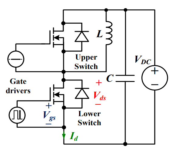 Discovering New and Advanced Methodology for Determining the Dynamic Characterization of Wide Bandgap DevicesSaumitra Jagdale15 March 20242462
For a long era, silicon has stood out as the primary material for fabricating electronic devices due to its affordability, moderate efficiency, and performance capabilities. Despite its widespread use, silicon faces several limitations that render it unsuitable for applications involving high power and elevated temperatures. As technological advancements continue and the industry demands enhanced efficiency from devices, these limitations become increasingly vivid. In the quest for electronic devices that are more potent, efficient, and compact, wide bandgap materials are emerging as a dominant player. Their superiority over silicon in crucial aspects such as efficiency, higher junction temperatures, power density, thinner drift regions, and faster switching speeds positions them as the preferred materials for the future of power electronics.
Read More A Comprehensive Guide to FPGA Development BoardsUTMEL11 September 202514296
This comprehensive guide will take you on a journey through the fascinating world of FPGA development boards. We’ll explore what they are, how they differ from microcontrollers, and most importantly, how to choose the perfect board for your needs. Whether you’re a seasoned engineer or a curious hobbyist, prepare to unlock new possibilities in hardware design and accelerate your projects. We’ll cover everything from budget-friendly options to specialized boards for image processing, delve into popular learning paths, and even provide insights into essential software like Vivado. By the end of this article, you’ll have a clear roadmap to navigate the FPGA landscape and make informed decisions for your next groundbreaking endeavor.
Read More Applications of FPGAs in Artificial Intelligence: A Comprehensive GuideUTMEL29 August 20253560
This comprehensive guide explores FPGAs as powerful AI accelerators that offer distinct advantages over traditional GPUs and CPUs. FPGAs provide reconfigurable hardware that can be customized for specific AI workloads, delivering superior energy efficiency, ultra-low latency, and deterministic performance—particularly valuable for edge AI applications. While GPUs excel at parallel processing for training, FPGAs shine in inference tasks through their adaptability and power optimization. The document covers practical implementation challenges, including development complexity and resource constraints, while highlighting solutions like High-Level Synthesis tools and vendor-specific AI development suites from Intel and AMD/Xilinx. Real-world applications span telecommunications, healthcare, autonomous vehicles, and financial services, demonstrating FPGAs' versatility in mission-critical systems requiring real-time processing and minimal power consumption.
Read More 800G Optical Transceivers: The Guide for AI Data CentersUTMEL24 December 20253641
The complete guide to 800G Optical Transceiver standards (QSFP-DD vs. OSFP). Overcome supply shortages and scale your AI data center with Utmel Electronic.
Read More Xilinx FPGAs: From Getting Started to Advanced Application DevelopmentUTMEL09 September 20254249
This guide is your comprehensive roadmap to understanding and mastering the world of Xilinx FPGA technology. From selecting your first board to deploying advanced AI applications, we'll cover everything you need to know to unlock the potential of these remarkable devices. The global FPGA market is on a significant growth trajectory, expected to expand from USD 8.37 billion in 2025 to USD 17.53 billion by 2035. This surge is fueled by the relentless demand for high-performance, adaptable computing in everything from 5G networks and data centers to autonomous vehicles and the Internet of Things (IoT). This guide will walk you through the key concepts, tools, and products in the Xilinx ecosystem, ensuring you're well-equipped to be a part of this technological revolution.
Read More
Subscribe to Utmel !
![1EDI20I12MFXUMA1]() 1EDI20I12MFXUMA1
1EDI20I12MFXUMA1Infineon Technologies
![UCC5350SBDR]() UCC5350SBDR
UCC5350SBDRTexas Instruments
![SI8261BCC-C-IS]() SI8261BCC-C-IS
SI8261BCC-C-ISSilicon Labs
![ATSHA204A-XHDA-T]() ATSHA204A-XHDA-T
ATSHA204A-XHDA-TMicrochip Technology
![HCS362-I/SN]() HCS362-I/SN
HCS362-I/SNMicrochip Technology
![HCNW3120-000E]() HCNW3120-000E
HCNW3120-000EBroadcom Limited
![FLC01-200B-TR]() FLC01-200B-TR
FLC01-200B-TRSTMicroelectronics
![ISO5451QDWRQ1]() ISO5451QDWRQ1
ISO5451QDWRQ1Texas Instruments
![FM31256-GTR]() FM31256-GTR
FM31256-GTRCypress Semiconductor Corp
![FOD3180]() FOD3180
FOD3180ON Semiconductor


 Product
 Brand
Brand Articles
 Tools
Tools


