7 Common Functions of MOSFET Gate Circuits

Gate drive circuits for MOSFET and IGBT
Overview:
MOSFETs are a type of voltage control device that have a number of benefits, including quick switching speed, high-frequency performance, high input impedance, low noise, low driving power, big dynamic range, and a large safe operating region (SOA). Switching power supplies, motor control, power tools, and other sectors all use it. The gate is the MOSFET's weakest component. It is possible to cause the device or even the system to fail if the circuit is not constructed appropriately. As a result, this article organizes the most popular gate circuits for your reference and discussion, and you are also free to share your own thoughts.
The common functions of MOSFET gate circuits are as follows:
1. Remove the noise coupled into the circuit and improve the reliability of the system;
2. Accelerate the conduction of MOSFET and reduce conduction loss;
3. Accelerate the turn-off of the MOSFET and reduce the turn-off loss;
4. Reduce MOSFET DI/DT, protect MOSFET and suppress EMI interference;
5. Protect the grid to prevent grid breakdown under abnormal high voltage conditions;
6. Increase the driving ability, and can drive the MOSFET under a smaller signal.
The function of the gate circuit that I can conceive of is as follows. You are free to submit your own suggestions. I'll also include the relevant circuit for everyone to debate here.
First, let's discuss the power IC's direct drive. Our most typical direct-drive method is depicted in the diagram below. Because we haven't done any processing on the drive circuit in this technique, we should aim to improve it when we do PCB LAYOUT. To reduce parasitic inductance and eliminate noise, shorten the gate trace from the IC to the MOSFET. increase the trace width, and locate Rg as far away from the MOSFET gate as practicable.
01 Direct drive
First and foremost, let's discuss the power IC's direct drive. The most popular direct drive method is depicted in the diagram below. We haven't done much processing in the drive circuit in this technique, therefore we should strive to optimize it when we do PCB LAYOUT. To reduce parasitic inductance and eliminate noise, shorten the gate trace from the IC to the MOSFET. increase the trace width, and locate Rg as far away from the MOSFET gate as practicable.
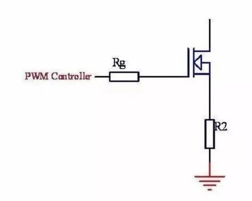
Of course, another factor to consider is the PWM CONTROLLER's driving capacity. The drive will be too sluggish, the switching loss will be too large, or the IC will be impossible to drive when the MOSFET is larger than the IC drive capabilities. This is when we need to pay attention to our designs.
02 When the internal driving capability of the IC is insufficient
Of course, the following solutions can also be used to remedy the problem of insufficient driving capabilities within the IC,
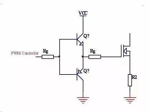
This method of enhancing driving capability not only extends on-time, but also shortens off-time, and has some effect on glitches and power loss control. Naturally, in LAYOUT, we should strive to position these two tubes as close to the MOSFET's gate as possible. The benefit is that the parasitic inductance is reduced and the circuit's anti-interference is improved.
03 Increase the turn-off speed of the MOSFET
If we just want to improve the MOSFET's turn-off speed, we can do so in the following way.
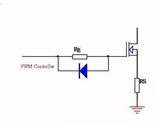
The MOSFET input capacitance can be discharged faster when the turn-off current is relatively high, decreasing turn-off losses. Low output impedance MOSFETs or N-channel negative cut-off voltage devices, such as jerk diodes, can be employed to obtain large discharge currents.
The voltage drop created by the current on the resistor when the gate is switched off is greater than the voltage drop when the diode is turned on. The diode will be turned on at this point, bypassing the resistance. The diode is in the circuit once it is turned on and the current diminishes. The effect of this circuit is shrinking, and the effect of this circuit will considerably lower the MOSFET turn-off delay time.
Of course, this circuit has several flaws, such as the fact that the gate current must still flow through the IC's output drive impedance. What is the answer?
Let's look at the PNP accelerated turn-off driving circuit in more detail.
04 PNP accelerates turn-off drive circuit
Let's take a look at the PNP rapid shutdown circuit below:

Currently, the PNP rapid turn-off circuit is the most popular. An instantaneous gate-source short circuit can be established under the action of the accelerating triode, resulting in the minimum discharge time. The diode is included to protect the triode's base on the one hand and to provide a loop and bias for the conduction current on the other.
The advantage of this circuit is that it may approach the push-pull action, and the acceleration effect is visible; but, because it goes through two PN junctions, the gate cannot truly reach 0 volts.
05 Drive when source output is high voltage
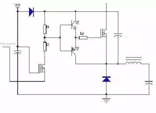
To achieve the circuit's goal when the source output is a high voltage, we must utilize a bias circuit. As illustrated in the diagram below, we utilize the source as a reference point to design a bias circuit, the driving voltage swings between the two voltages, and the driving voltage deviation is determined by the Low voltage supply.
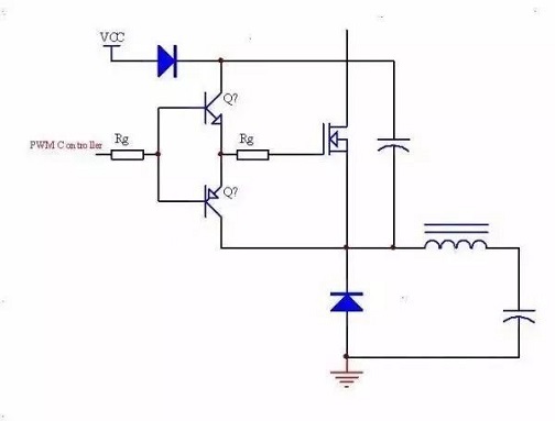
Of course, something is amiss with this image; I'm not sure if anyone can see it. In actuality, the issue is that the "drive power" must be turned off, and the MOS source must be "grounded" (to give everyone a deeper impression).
For your convenience, I've included the right drawing:
06 Drivers that meet isolation requirements
Transformer drives are frequently utilized to offer high-side floating gate drives or to meet safety isolation requirements. As indicated in the diagram, this drive isolates the drive control and MOSFET and can be used in both low-voltage and high-voltage circuits.
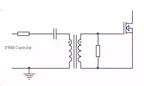
Of course, there are special driver IC s that can fix the problem, but the transformer driver has its own set of qualities that make many people insist on using it.
The coupling capacitor in the illustration serves as a reset voltage for the magnetized core. Magnetic saturation will occur if this capacitor is not there.
The purpose of the resistor in series with the capacitor is to prevent the LC from oscillating due to an abrupt change in duty cycle, hence this resistor is included.
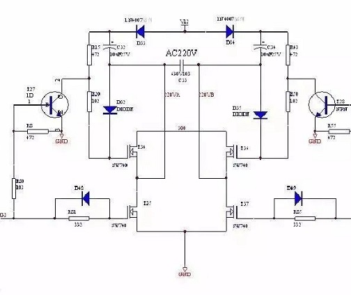
07 Bootstrap Inversion Diagram
Below is an actual bootstrap inversion diagram for reference:
1. What is the role of the MOSFET gate?
Controls the pinch-off and on-resistance of the conduction channel between drain and source.
2. Where does the name: gate, source and drain comes from?
The gate is equivalent to a gate (switch) VG is bigger than the VT tube conduction, the source is the place where the electrons come from, and the drain is the place where the electrons disappear (leak).
3. Why do mos tubes need gate drive circuits?
The MOS tube is driven by voltage, but there is a small "capacitor" between the GS poles of the MOS tube. It takes a certain amount of time to charge this capacitor. In principle, the faster the charging process, the better. The slower the charging process, the better the heat of the MOS tube, which is serious. will burn directly. The function of the gate drive circuit is to make the "capacitor" charge faster and make the MOS transistor turn on or off faster.
 Modeling Wide Band-Gap Semiconductors for Enhanced PerformanceRakesh Kumar, Ph.D.31 January 20243464
The article delves into the challenges faced by silicon-based power electronic devices and highlights the potential of wide band-gap semiconductors. It also emphasizes the importance of modeling power semiconductor devices and provides insights into various models. For electrical energy conversion to be dependable and effective, power electronics and semiconductor device technologies are essential.
Read More Optimizing Energy Management with Non-Isolated DC-DC ConvertersRakesh Kumar, Ph.D.04 February 20243106
The article classifies DC-DC converters and discusses the benefits and limitations of them. It proposes a modified DC-DC converter topology that combines the Cuk and Positive Output Super Lift Luo topologies to achieve a higher voltage gain with fewer components.
Read More ‘6G Networks’ - Pioneering the Next Era of Connectivity And InnovationRakesh Kumar, Ph.D.18 March 20243448
The article provides a comprehensive overview of the evolving landscape of mobile networks, the requirements that will shape the future of mobile communication, and the innovative technologies driving the transition to 6G.
Read More Review of IoT-Based Smart Home Security Systems- Part 1Rakesh Kumar, Ph.D.28 March 20243807
The article discusses the evolution of IoT-based smart home security systems, integrating advanced technologies like Raspberry Pi, PIR sensors, and voice recognition for enhanced user experience and efficiency.
Read More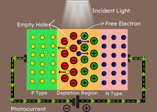 Understanding Photodiodes: Working Principles and Applications - Part 2Rakesh Kumar, Ph.D.24 May 20244816
The article provides a comprehensive overview of photodiodes, focusing on their operational principles, key factors affecting their efficiency, advantages, and disadvantages, and highlights their diverse applications.
Read More
Subscribe to Utmel !
![CR0180-000]() CR0180-000
CR0180-000TE Connectivity
![214355]() 214355
214355TE Connectivity
![072160-230-2EB]() 072160-230-2EB
072160-230-2EBMenda
![16-6040-0062]() 16-6040-0062
16-6040-0062Amphenol
![S200-2-00CS2904]() S200-2-00CS2904
S200-2-00CS2904TE Connectivity
![S-5844A65CB-A4T2U3]() S-5844A65CB-A4T2U3
S-5844A65CB-A4T2U3SII Semiconductor
![B-070-19-10]() B-070-19-10
B-070-19-10TE Connectivity
![42510]() 42510
42510SK Hand Tool
![RMA791]() RMA791
RMA791Chip Quik
![FLS99-4G]() FLS99-4G
FLS99-4GSRA Soldering


 Product
 Brand
Brand Articles
 Tools
Tools


