A Study of the Interelectrode Capacitances of SiC and GaN Power Semiconductor Devices Using Multiple Current Probes
When it comes to high switching speed, low on-state resistance, high operating temperature, etc, a considerable deal of research has been drawn to SiC/GaN-based devices over the past few years. This results in smoother functioning for high-power applications with even lower operating costs as compared to the traditional silicon (Si) based semiconductor devices. As a result, SiC and GaN support applications in reusable energy, HEMTs, high power industrial equipments, etc.
Power Semiconductor devices have voltage-dependant interelectrode capacitances that have a crucial role in the commutation on switching losses as well as electromagnetic compatibility (EMC).

Fig 1a: Normally-on GaN HEMT Fig 1b: Normally-off» SiC JFET
The above figure 1a shows the normally-on condition of GaN HEMT with capacitances Cgd, Cgs, and Cds and figure 1b shows the normally-off condition with capacitances Cgd and Cgs. During the experiment, it was noted that C-VDS curves were always given for one VGS voltage value. It is impossible to get accurate information in linear coordinates in high VDS voltage due to the strong nonlinearity of the interelectrode capacitances. Therefore, researchers and engineers must be able to characterize these capacitances easily, which can be applied to modeling of power devices.
Two-current-probe method Principle
It is essential to devise a new arrangement that can be easily operated by researchers to characterize the capacitances in Sic and GaN power semiconductor devices. Hence, the arrangement to compute an unknown impedance Zx is portrayed in figure 2.
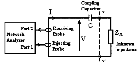
Figure 2- Basic Setup for two current probe measurements
In this figure a vector network analyzer, a current receiving probe, and a current injection probe are used. With the help of an equivalent transformer model for current probes, equation 1 can be formulated as

Equation 1- Impedance Equation
Here, network analyzers probe and measure S-parameters S11 and S21. Whereas K and Zsetup are the two parameters that describe the coupling effect between current probes and the connecting wires, and the impedance of the measurement configuration respectively.
In order to determine the value for these parameters, we replace ZX in equation 1 with two precision standard resistors to obtain two equations. By resolving these equations to find K and Zsetup, this arrangement can be used to find unknown impedance Zx.
Measurement Results
Figure 4 shows the measured capacitances of the JFET using multi-probe method. SiC JFET interelectrode capacitances show a correlation both with VDS and VGS, as shown in the results.
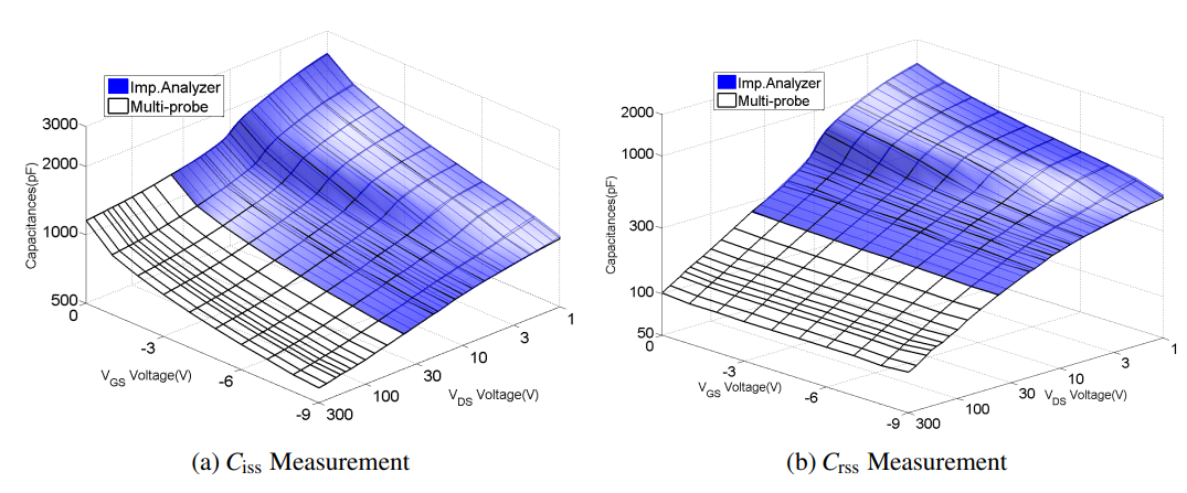
Fig 3: Capacitances measured
Under 40 volts, the surfaces could be seen to almost overlap, implying that low voltages could easily be detected and passed through the probes. Moreover, the multiprobe method allows for a higher VDS voltage than the impedance analyzer with a 40V bias VDS voltage limit.
Three-current-probe method Principle
The main issue with the two-current probe method is the accuracy limitation which is subdued by the new three-current probe method. This uses one additional current probe with one CIP and two CRPs to directly compute inter-electrode capacitances as shown in figure 4a.
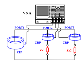
Figure 4a- Preliminary Setup
However for this setup to work, it is essential to form an equivalent circuit of measurement as shown in figure 4b. Here, the signal source of port 1 is V1 whereas Vp1, Vp2, and Vp3 are resultant signal voltages measured at their respective ports.
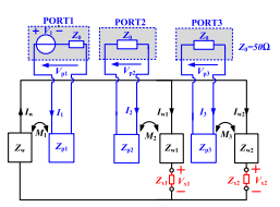
Figure 4b- Equivalent Circuit
Keeping the output and input impedance of all ports at 50, Zp1, Zp2, and Zp3 are input impedances of injection and receiving probes respectively. The mutual inductance between the probe and circuit is represented by M1, M2, and M3, whereas the Zw, Zw1, and Zw2 depict the parasitic impedance of wire connections. According to Ohms's law, voltage V1 induces a current IW in the circuit through the injection probe.
From figure 4b, a matrix(shown in figure 5) can be formulated that uses Kirchoff's voltage law to find unknown impedances Zx1 and Zx2.

Figure 5- Formulated Matrix
The unknown impedances Zx1 and Zx2 can be represented as shown in figure 6.


Figure 6- Impedance Equation
The network analyzer measures the S parameters whereas with the help of six precision standard resistors coupling effects Q1 and Q2 between the probes and measurement configuration can be obtained.
Measurement Results
The below figures 5a and 5b show the Cds impedance and phase measurement results when VDS equals to 0V and 20V respectively.

Fig 5a: Cds measurement result Fig 5b: Cgd measurement result
As demonstrated in the results, both Cds and Cgd are close to noise levels at 1MHz, which makes calculating the capacitance at 1MHz difficult. GaN HEMTs have such small interelectrode capacitances that their measured impedance around 1MHz is quite big, leading to measurement insufficiency.
Conclusion
A technical study on the use of multi-probe method in measuring voltage-dependent inter-electrode capacitances of SiC/GaN semiconductor devices was conducted. During the experiment, a basic setup was done wherein the proposed method has the advantage of isolating the measurement equipments from the DC bias power source. During the «Normally-off» condition of the SiC JFET, the method allows the characterization of the inter-electrode capacitances. This characterization takes place in high bias VDS voltage and the measurement results prove the accuracy of this method. Contrarily, the measurement results for «Normally-on» GaN HEMT may not occur, as the inter-electrode impedance around 1MHz makes the received current by the CRP so small that the results are almost noise. In order to counter these inconveniences, two CRPs are wound with more turns in order to increase their measurement sensitivity. The results obtained proved that this modification greatly enhances the measurement precision for small inter-electrode capacitance values. This application can be successfully used in traditional silicon power devices as well along with their inter-electrode characterization.
 UTMEL 2024 Annual gala: Igniting Passion, Renewing BrillianceUTMEL18 January 20244518
As the year comes to an end and the warm sun rises, Utmel Electronics celebrates its 6th anniversary.
Read More Electronic Components Distributor Utmel to Showcase at 2024 IPC APEX EXPOUTMEL10 April 20245489
Utmel, a leading electronic components distributor, is set to make its appearance at the 2024 IPC APEX EXPO.
Read More Electronic components distributor UTMEL to Showcase at electronica ChinaUTMEL07 June 20244089
The three-day 2024 Electronica China will be held at the Shanghai New International Expo Center from July 8th to 10th, 2024.
Read More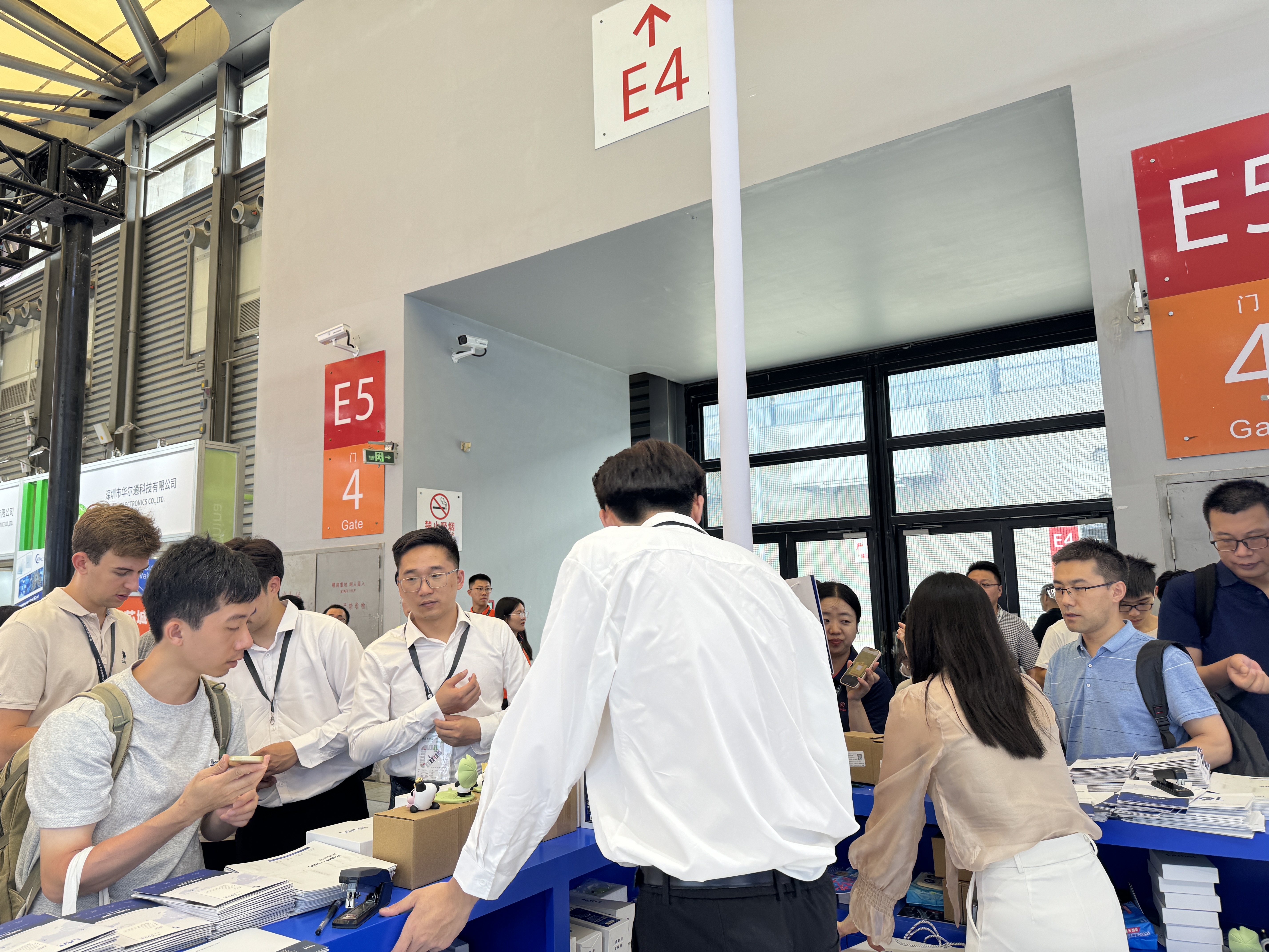 Electronic components distributor UTMEL Stands Out at electronica china 2024UTMEL09 July 20244455
From July 8th to 10th, the three-day electronica china 2024 kicked off grandly at the Shanghai New International Expo Center.
Read More A Combo for Innovation: Open Source and CrowdfundingUTMEL15 November 20195044
Open source is already known as a force multiplier, a factor that makes a company's staff, financing, and resources more effective. However, in the last few years, open source has started pairing with another force multiplier—crowdfunding. Now the results of this combination are starting to emerge: the creation of small, innovative companies run by design engineers turned entrepreneurs. Although the results are just starting to appear, they include a fresh burst of product innovation and further expansion of open source into business.
Read More
Subscribe to Utmel !
![AMEOF15-12SL277NZ]() AMEOF15-12SL277NZ
AMEOF15-12SL277NZaimtec
![AMES15-3S277NZ-Q]() AMES15-3S277NZ-Q
AMES15-3S277NZ-Qaimtec
![AMEM3-15S277HAVZ-ST]() AMEM3-15S277HAVZ-ST
AMEM3-15S277HAVZ-STaimtec
![AMES100-12SNZ-Q]() AMES100-12SNZ-Q
AMES100-12SNZ-Qaimtec
![AMEL15-12S277UNZ-B]() AMEL15-12S277UNZ-B
AMEL15-12S277UNZ-Baimtec
![AME15-12S277VZ]() AME15-12S277VZ
AME15-12S277VZaimtec
![AMES50-15SNZ]() AMES50-15SNZ
AMES50-15SNZaimtec
![AME25-5S277VZ-60]() AME25-5S277VZ-60
AME25-5S277VZ-60aimtec
![AME15-15SMAZ-100]() AME15-15SMAZ-100
AME15-15SMAZ-100aimtec
![AME15-9SVZ-STD]() AME15-9SVZ-STD
AME15-9SVZ-STDaimtec


 Product
 Brand
Brand Articles
 Tools
Tools


