Product
 Brand
Brand Articles
 Tools
Tools
Introduction to Semiconductor Devices

What Is A Semiconductor?
Catalog
I Introduction
The semiconductor materials of semiconductor devices are silicon, germanium, or gallium arsenide, which can be used as rectifiers, oscillators, light emitters, amplifiers, photometers, and other equipment. To distinguish them from integrated circuits, they are sometimes called discrete devices. The basic structure of most two-terminal devices (i.e., crystal diodes) is a PN junction.
Semiconductor devices usually use different semiconductor materials, different processes, and geometries. A wide variety of crystal diodes with different functions have been developed. The frequency coverage of crystal diodes can range from low and high frequency, microwave, millimeter-wave, and infrared to lightwave. Three-terminal devices are generally active devices, which are typically represented by various transistors (also known as crystal transistors). Transistors can be divided into two types: bipolar transistors and field-effect transistors. According to different uses, transistors can be divided into power transistors, microwave transistors, and low-noise transistors. In addition to general transistors for amplification, oscillation, and switching, there are also some special-purpose transistors, such as phototransistors, magneto-sensitive transistors, and field-effect sensors. These devices can not only convert the information of some environmental factors into electrical signals but also have the amplification effect of ordinary transistors to obtain larger output signals. Besides, there are some special devices, such as single-junction transistors that can be used to generate sawtooth waves. Thyristors can be used in various large current control circuits, and charge-coupled devices can be used as signal processing devices or information storage devices.
In military equipment such as communications and radar, weak signals are primarily received by semiconductor receivers with high sensitivity and low noise. With the rapid development of microwave communication technology, low-noise devices for microwave semiconductors have developed rapidly. The operating frequency has been continuously increased, and the noise figure has been continuously reduced. Microwave semiconductor devices have been widely used in air defense and anti-missile, electronic warfare and other systems due to their excellent performance, small size, lightweight, and low power consumption.
II Classification
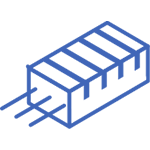
1. Crystal diode
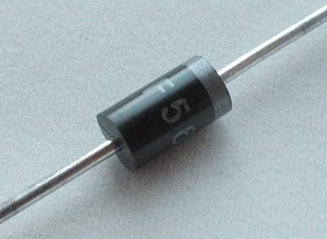
Figure 1. Crystal diode
The basic structure of a crystal diode is a combination of a P-type semiconductor and an N-type semiconductor that form a PN junction. At the interface of the PN junction, since the holes in the P-type semiconductor and the electrons in the N-type semiconductor tend to diffuse to each other, a dipole layer with space charge is formed. This dipole layer prevents the continued diffusion of holes and electrons and brings the PN junction to an equilibrium state. When the P terminal (P-type semiconductor side) of the PN junction is connected to the positive electrode of the power supply and the other end is connected to the negative electrode, holes and electrons flow to the dipole layer, which will make the dipole layer thinner, and the current rises quickly. If the direction of the power supply is reversed, holes and electrons flow away from the dipole layer and then make the dipole layer thicker. At the same time, the current is limited to a small saturation value (called the reverse saturation current). Therefore, the PN junction has unidirectional conductivity. Also, the dipole layer of the PN junction functions as a capacitor, which changes with the applied voltage. The electric field is strong inside the dipole layer. When the applied reverse voltage reaches a certain threshold, avalanche breakdown occurs inside the dipole layer and the current suddenly increases by several orders of magnitude.
Diodes that use the characteristics of PN junctions in various applications are rectifier diodes, detection diodes, frequency conversion diodes, varactor diodes, switching diodes, Zener diodes, and breakdown diodes (collision avalanche transition diodes) and capture diodes (capturing plasma avalanche transit-time diodes). Besides, there are tunnel diodes that take advantage of the special effects of PN junctions, Schottky diodes and Gunn diodes without PN junctions.
2. Bipolar transistor
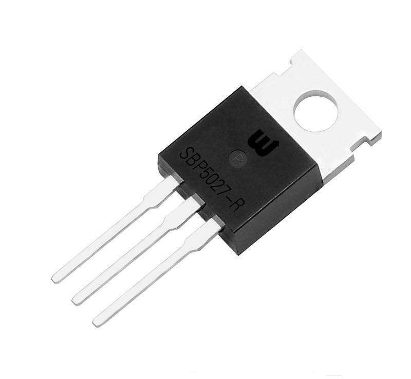
Figure 2. Bipolar transistor
It is composed of two PN structures, one of which is called an emitting junction and the other is called a collector junction. A thin layer of semiconductor material between the two junctions is called the base region. The two electrodes connected to one end of the emitter junction and one end of the collector junction are called the emitter and collector, respectively. The electrode connected to the base region is called the base. In application, the emitter junction is forward biased and the collector is reverse biased. A large number of minority carriers are injected into the base region by the current at the emitting junction. These minority carriers diffuse to the collector junction to form a collector current. Only a small number of minority carriers recombine in the base region and form a base current. The ratio of the collector current to the base current is called the common-emitter current amplification factor. In the common-emitter circuit, a small change in the base current can control a large change in the collector current, which is the current amplification effect of a bipolar transistor. Bipolar transistors can be divided into two types, NPN and PNP.
3. Field-effect transistor
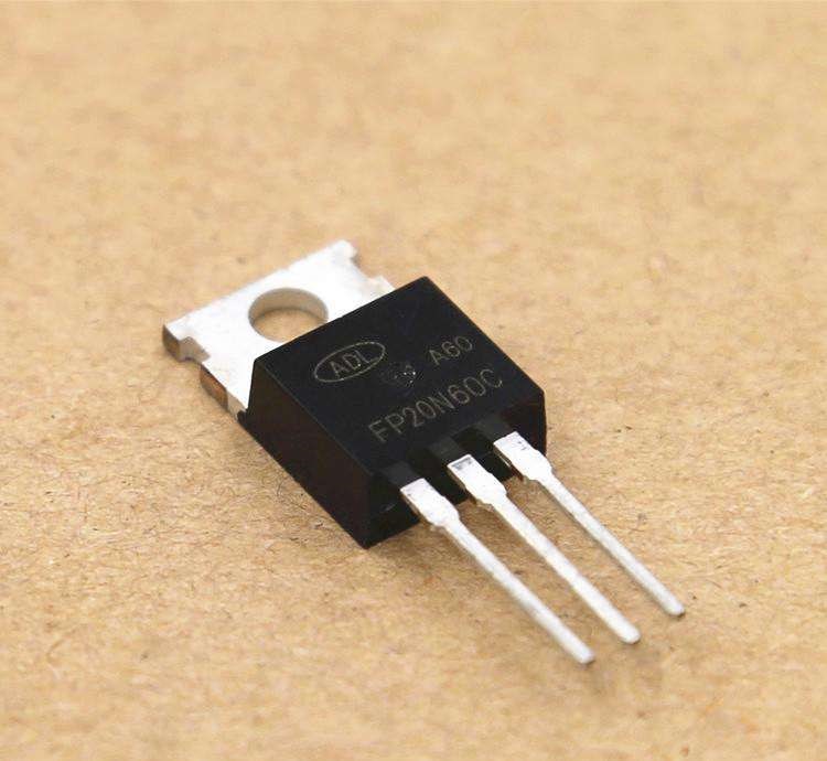
Figure 3. Field-effect transistor
The field-effect transistor relies on a thin layer of semiconductor being affected by the lateral electric field to change its resistance (field effect for short) so that it has the function of amplifying signals. This thin layer of semiconductor is connected to two electrodes at both ends called source and drain. The electrode that controls the lateral electric field is called the gate.
According to the structure of the gate, field-effect transistors can be divided into three types:
① Junction field effect transistor (uses PN structure as a gate);
② MOS field-effect transistor (metal-oxide-semiconductor gate);
③ MES FET (Metal and semiconductor contact to form the gate);
MOS FET is the most widely used. Especially in the development of large-scale integrated circuits, MOS large-scale integrated circuits have special advantages. MES field-effect transistors are commonly used in GaAs microwave transistors.
Based on MOS devices, a charge-coupled device (CCD) has been developed. It uses the charge stored near the semiconductor surface as information and controls the potential well near the surface to transfer the charge in a certain direction near the surface. This kind of device can usually be used as a delay line and a memory, etc.; it can also be used as an image sensor with a photodiode array.
III Nomenclature of semiconductor device
1. Chinese semiconductor device model nomenclature
The semiconductor device model consists of five parts (field-effect devices, special semiconductor devices, composite tubes, PIN tubes, and laser devices only consist of three parts, which are the third, fourth, and fifth parts). The five sections are as follows:
Part 1: The number of effective electrodes of a semiconductor device is represented by a number. 2-diode, 3-triode
Part 2: Use the Chinese phonetic alphabet to indicate the material and polarity of semiconductor devices. When the diode is displayed: A-N type germanium material, B-P type germanium material, C-N type silicon material, D-P type silicon material. When the triode is shown: A-PNP type germanium material, B-NPN type germanium material, C-PNP type silicon material, D-NPN type silicon material.
Part 3: Use Chinese pinyin to indicate the type of semiconductor device. P-common tube, V-microwave tube, W-regulator tube, C-parameter tube, Z-rectifier tube, L-rectifier stack, S-tunnel tube, N-damping tube, U-photoelectric device, K-switch tube, X-low frequency low power tube (f<3MHz, Pc<1W), G-high frequency low power tube (f>3MHz, Pc<1W), D-low frequency high power tube (f<3MHz, Pc>1W), A-high frequency high power tube (f>3MHz, Pc>1W), T-semiconductor thyristor (Controllable Rectifier), Y-body effect device, B-avalanche tube, J-step recovery tube, CS-field effect tube, BT-semiconductor special device, FH-composite tube, PIN-PIN tube, JG-laser device.
Part 4: Use the number to represent the serial number
Part 5: Use Chinese Pinyin to indicate the specification number
For example, 3DG18 means NPN silicon material high-frequency transistor
2. Japanese semiconductor discrete device model nomenclature
Semiconductor discrete devices produced in Japan, consisting of five to seven parts. Usually, only the first five parts are used, and the symbols of each part have the following meanings:
Part 1: Use the number to indicate the number or type of effective electrodes of the device. 0-photoelectric (i.e., photosensitive) diode triode and the combination of the above devices, 1-diode, 2-triodes or other devices with two PN junctions, 3-other devices with four active electrodes or three PN junctions, and so on.
Part 2: Japan Electronics Industry Association JEIA registration mark. S- indicates a semiconductor discrete device registered with the Japan Electronics Industry Association JEIA.
Part 3: Use letters to indicate the polarity and type of materials used in the device. A-PNP HF tube, B-PNP LF tube, C-NPN HF tube, D-NPN LF tube, F-P thyristor, G-N thyristor, H-N base single-junction transistor, J-P channel FET, K-N channel FET, M-triac.
Part 4: Use the number to indicate the serial number registered in the Japan Electronics Industry Association JEIA. Two or more integers-starting with "11", indicating the serial number registered in the Japan Electronics Industry Association JEIA; devices with the same performance of different companies can use the same serial number; the larger the number, the newer the product.
Part 5: Use the letters to indicate the improved product logo of the same model. A, B, C, D, E, F indicate that this device is an improved product of the original model.
3. US Semiconductor Discrete Device Model Nomenclature
American transistor or other semiconductor device nomenclature is more complex. The American Electronics Industry Association semiconductor discrete device naming method is as follows:
Part 1: Use the symbol to indicate the type of device use. JAN-military grade, JANTX-special military-grade, JANTXV-super special military-grade, JANS-space category, (none)-non-military supplies.
Part 2: The number of PN junctions. 1-diode, 2-transistor, 3-three PN junction devices, n-n PN junction devices.
Part 3: American Electronics Industry Association (EIA) registration mark. N-This device is registered with the American Electronics Industry Association (EIA).
Part 4: American Electronics Industry Association registration sequence number. The multi-digit number-The serial number of the device registered with the American Electronics Industry Association.
Part 5: Use letters to indicate device binning. A, B, C, D – different grades of the same model.
For example, JAN2N3251A means PNP silicon high-frequency low power switch transistor, JAN-military grade, 2-transistor, N-EIA registration mark, 3251-EIA registration sequence number, A-2N3251A file.
4. International Electronic Federation Semiconductor Device Model Nomenclature
European countries such as Germany, France, Italy, the Netherlands, Belgium, and Eastern European countries such as Hungary, Romania, Yugoslavia, and Poland all use the International Electronic Federation semiconductor discrete device model naming method. This naming method consists of four basic parts, and the symbols and meanings of each part are as follows:
Part 1: Use letters to indicate the materials used in the device. A-the forbidden bandwidth of materials used in devices is Eg=0.6-1.0eV, such as germanium. B-the forbidden bandwidth of materials used in devices is Eg=1.0-1.3eV, such as silicon. C-the materials used in devices are Eg>1.3eV, such as gallium arsenide. D-Eg<0.6eV for device materials, such as indium antimonide. E-devices for composite materials, and materials for photovoltaic cells
Part 2: Use letters to indicate the type and main characteristics of the device. A-detection switch mixing diode, B-variable diode, C-low frequency low power transistor, D-low frequency high power transistor, E-tunnel diode, F-high frequency low power transistor, G-composite device and other devices, H-Magneto-sensitive diode, K-Hall element in the open magnetic circuit, L-high-frequency high-power triode, M-Hall element in the closed magnetic circuit, P-photosensitive device, Q-light-emitting device, R-low power thyristor, S-small power switch, T-high power thyristor, U-high power switch, X-multiplier diode, Y-rectifier diode, Z-Zener diode.
Part 3: Represent the registration number with numbers or letters plus numbers. Three digits-represents the registration number of a general-purpose semiconductor device, and one letter plus two digits-represents the registration number of a dedicated semiconductor device.
Part 4: Use letters to bin the same type number of devices. A, B, C, D, E – marks indicating that the devices of the same model are classified according to a certain parameter.
In addition to the four basic parts, suffixes are sometimes added to distinguish characteristics or further classify them. The common suffixes are as follows:
1. The suffix of the Zener diode model. The first part of the suffix is a letter, which indicates the allowable tolerance range of the stable voltage value. The letters A, B, C, D, and E indicate that the allowable tolerance is ±1%, ±2%, ±5%, ±10%, ±15%; the second part of the suffix is a number, which represents the integer value of the nominal stable voltage; the third part of the suffix is the letter V, which represents the decimal point, and the number after the letter V is the decimal value of the nominal stable voltage of the voltage regulator.
2. The suffix of the rectifier diode is a number, which indicates the maximum reverse peak withstand voltage of the device, the unit is volts.
3. The suffix of the thyristor model is also a number, and the voltage value with the smaller value between the maximum reverse peak withstand voltage and the maximum reverse shutdown voltage is usually marked.
For example, BDX51- means NPN silicon low-frequency high-power transistor, AF239S- means PNP germanium high-frequency low-power transistor.
IV Integrated circuit
Crystal diodes, triodes, resistors, and capacitors are made on the same silicon chip, which is called an integrated circuit. Silicon chips with fewer than 100 components are called small-scale integrated circuits. Silicon chips with components from 100 to 1,000 are called medium-sized integrated circuits, and large-scale integrated circuits have the number of components from 1,000 to 100,000. Very-large-scale integration (VLSI) contains hundreds of thousands to millions of transistors.
2025 Update: As of 2024-2025, semiconductor technology has advanced significantly. Modern processors contain billions of transistors:
Nvidia's B100 GPU (2024) contains approximately 208 billion transistors
Apple's M3 Ultra (2025) contains 184 billion transistors
Industry leaders are targeting 1 trillion transistor chips by 2030-2034
Manufacturing processes have reached 2nm nodes, with Intel developing sub-1nm processes for the 2030s
Integrated circuits are the basic electronic devices necessary for the current development of computers and artificial intelligence systems. Many advanced industrial countries attach great importance to the development of the integrated circuit industry. The degree of integration of integrated circuits continues to increase, though at a pace slower than the traditional Moore's Law prediction. Advanced technologies such as extreme ultraviolet (EUV) lithography, 3D chip stacking, chiplet architectures, and nanosheet transistors are enabling continued progress in semiconductor performance and density.
V Optoelectronic devices
1. Photodetector
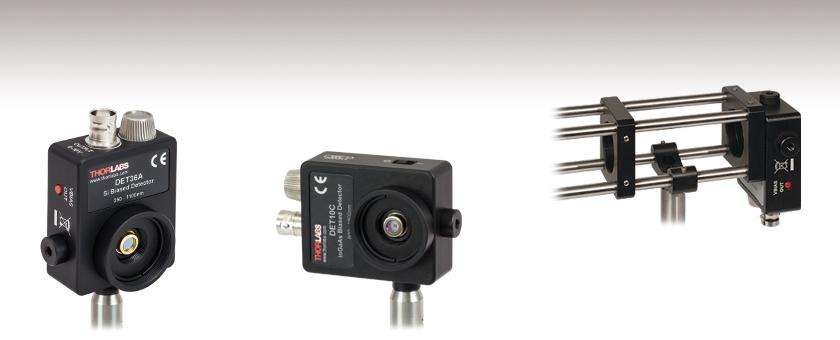
Figure 4. Photodetector
The function of the photodetector is to convert weak light signals into electrical signals, and then amplify the electrical signal through an amplifier, thereby achieving the purpose of detecting the optical signal. Photoresistors were one of the earliest developed photodetectors. They take advantage of the effect of reducing the resistance of a semiconductor when exposed to light. Besides, both photodiodes and photovoltaic cells can be used as photodetection elements. Weak light signals can be detected with avalanche photodiodes. It biases a PN junction under the bias close to avalanche. A small number of carriers excited by a weak light signal pass through the strong field region close to the avalanche. Due to the impact ionization, the number doubles, resulting in a larger electrical signal. In addition to photodetectors, there are similar particle detectors made of semiconductors.
2. Semiconductor light-emitting diode
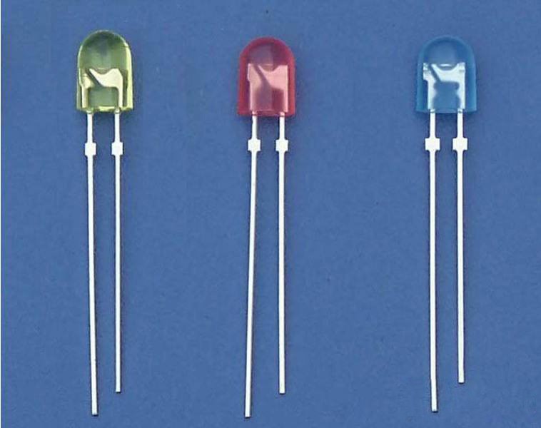
Figure 5. Semiconductor light-emitting diode
The structure of a semiconductor light-emitting diode is a PN junction. When a current is passed in the forward direction, the injected minority carriers emit light by recombination. It can emit green, yellow, red, and infrared light. The materials used are GaP, GaAs, GaAs1-xPx, Ga1-xAlxAs, In1-xGaxAs1-yPy, and the like.
3. Semiconductor laser
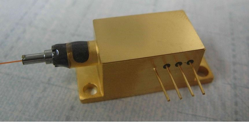
Figure 6. Semiconductor laser
If the light-emitting area of the high-efficiency semiconductor light-emitting device is located in an optical resonant cavity, a laser output can be obtained. Such devices are called semiconductor lasers or injection lasers. The earliest PN junctions used in semiconductor lasers were homojunctions, and double heterojunction structures were later adopted. The advantage of the double heterojunction laser is that it can confine the injected minority carriers in a very thin layer of the active area to emit light in combination. At the same time, the light waveguide composed of the double heterojunction structure can also confine the generated photons to this layer of the active area. Therefore, the double heterojunction laser has a lower threshold current density and can continuously operate at room temperature.
4. Photocell
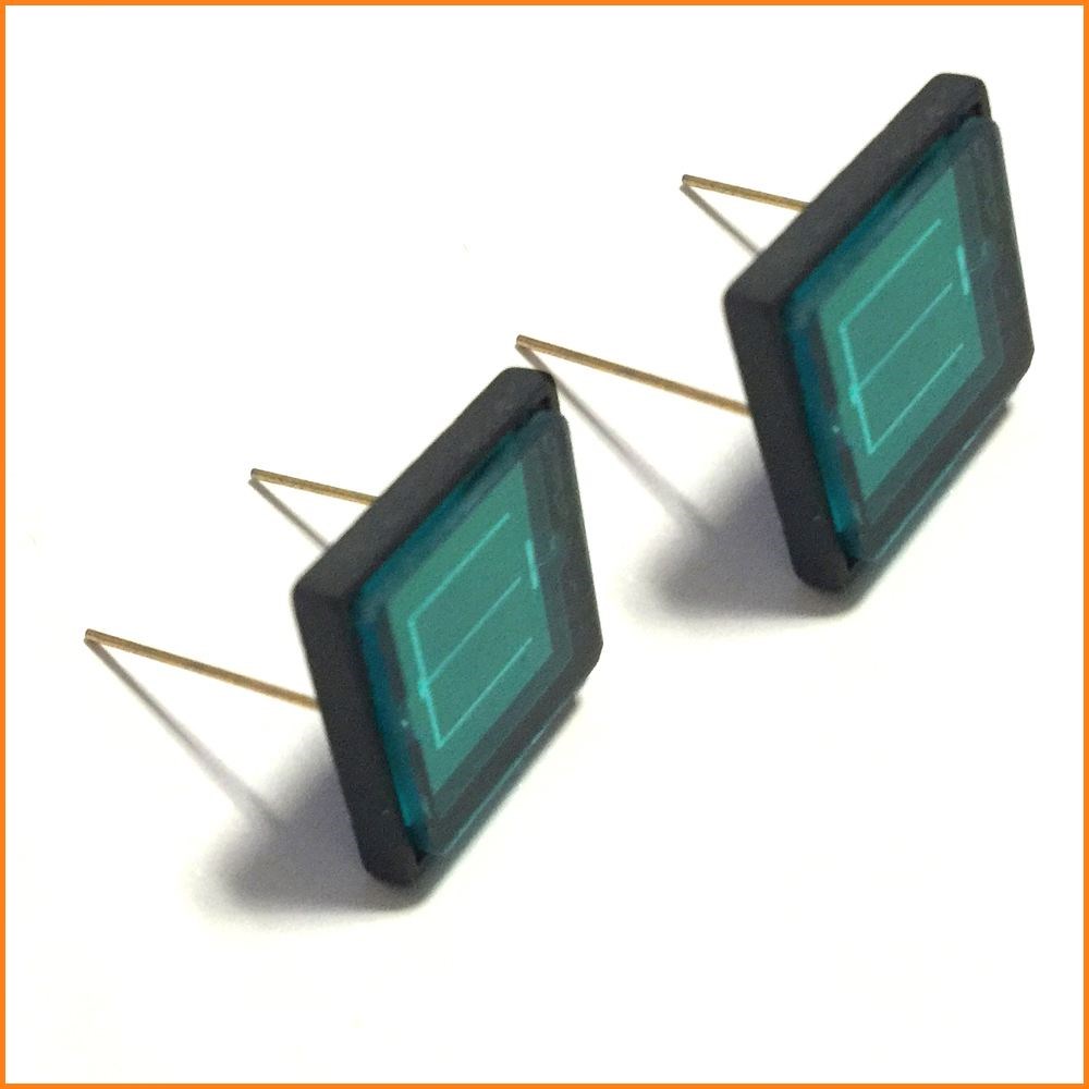
Figure 7. Photocell
When light is projected onto a PN junction, the electron-hole pairs excited by the light are separated in opposite directions by the internal electric field near the PN junction, so an electromotive force is generated at both ends of the PN junction, which becomes a photovoltaic cell. Solar cells that convert sunlight into electrical energy are highly valued. The first solar cells used were made of silicon single crystals, and the cost was too high to be widely used. Internationally, researchers are looking for low-cost solar cells. The materials used include polysilicon, amorphous silicon, and newer materials such as perovskites and organic photovoltaics.
5. Others
Devices made using other characteristics of semiconductors include thermistors, Hall devices, pressure-sensitive components, gas-sensing transistors, and surface-acoustic-wave devices.
VI Future development
Memorial Note: Gordon Moore, co-founder of Intel and creator of Moore's Law, passed away on March 24, 2023, at the age of 94. His vision and prediction have shaped the semiconductor industry for nearly six decades.
Moore's Law, first articulated in 1965, has been a guiding principle for the semiconductor industry for nearly 60 years. The birth of this law was a milestone in the history of semiconductor technology.
During these decades, Moore's Law has become a guiding light for the development of information technology. Computers have changed from mysterious and inaccessible behemoths to indispensable tools for most people. Information technology has entered countless ordinary homes from the laboratory. The Internet has connected the world, and multimedia audiovisual equipment has enriched everyone's life. This law determined that changes in information technology would accelerate and products would change faster and faster. People have seen that the innovation of technology and products generally follows its pace. Most of the pioneers became industry leaders, while the laggards were easily left behind.
The driving force behind all this is semiconductor chips. If transistors, resistors, and capacitors were separately mounted on circuit boards in the old way, not only would personal computers and mobile communications not have appeared, but even new technologies such as genome research, computer-aided design, and manufacturing would not be available. Relevant experts point out that Moore's Law is not just a law for chip technology; it has expanded to wireless technology, optical technology, sensor technology, and other fields, becoming a guiding ideology for people to explore and innovate in new domains.
Current Status (2024-2025): The debate about Moore's Law continues:
Traditional transistor scaling has slowed significantly since around 2010
In September 2022, Nvidia CEO Jensen Huang declared Moore's Law "dead"
Intel CEO Pat Gelsinger maintains the opposite view, believing innovation continues
The industry has adapted through new technologies: 3D chip stacking, chiplet architectures, advanced packaging (CoWoS, SoIC), extreme ultraviolet (EUV) lithography, and new transistor designs (FinFET, nanosheet transistors)
Energy-efficient performance has continued to improve at roughly threefold every two years
Manufacturing processes have reached 2nm nodes (IBM, TSMC), with Intel targeting sub-1nm "Angstrom Era" processes by the 2030s
There is no doubt that Moore's Law has had profound implications for the entire world. However, as transistor circuits approach their performance limits, traditional scaling faces significant challenges. Experts disagree on the timeline and nature of these limits. As early as the 2000s, concerns were raised about physical barriers at the nanoscale. Some predicted that 5nm processors might mark a significant challenge. Various industry leaders have offered different perspectives on when and how Moore's Law might evolve or end.
In recent years, Gordon Moore himself acknowledged that the pace of advancement was changing. Industry experts point out that even as traditional Moore's Law faces challenges, the pace of innovation in information technology has not slowed down. The focus has shifted from pure transistor density to overall system performance, energy efficiency, and specialized computing architectures.
The semiconductor industry continues to innovate through multiple approaches: advanced lithography techniques (including high numerical aperture EUV), new materials (such as gallium nitride and silicon carbide for power electronics), 3D integration, heterogeneous computing architectures, and specialized processors for artificial intelligence and machine learning. These innovations ensure that computational capabilities continue to advance, even as the traditional path of Moore's Law becomes more challenging.
The future of semiconductor technology lies not just in making transistors smaller, but in innovating across multiple dimensions: novel architectures, advanced packaging, new materials, quantum computing research, neuromorphic computing, and photonic integrated circuits. The industry's ability to continue delivering performance improvements through creative engineering and scientific breakthroughs demonstrates that while the original formulation of Moore's Law may be evolving, the spirit of continuous innovation it represented remains very much alive.
Article Updates: This article was originally published in 2020 and has been updated in 2025 to reflect current developments in semiconductor technology, including the status of Moore's Law, latest transistor counts, manufacturing processes, and the memorial of Gordon Moore who passed away in 2023.
 UTMEL
UTMEL
We are the professional distributor of electronic components, providing a large variety of products to save you a lot of time, effort, and cost with our efficient self-customized service. careful order preparation fast delivery service
What do you mean by semiconductor devices?
Semiconductor device, electronic circuit component made from a material that is neither a good conductor nor a good insulator (hence semiconductor). Such devices have found wide applications because of their compactness, reliability, and low cost.
What is Semiconductor give example?
A semiconductor material has an electrical conductivity value falling between that of a conductor, such as metallic copper, and an insulator, such as glass. ... Some examples of semiconductors are silicon, germanium, gallium arsenide, and elements near the so-called "metalloid staircase" on the periodic table.
What are the two types of semiconductor devices?
Semiconductors are materials that have properties of both normal conductors and insulators. Semiconductors fall into two broad categories: Intrinsic semiconductors are composed of only one kind of material; silicon and germanium are two examples. These are also called “undoped semiconductors” or “i-type semiconductors.
What is the purpose of semiconductor devices?
A semiconductor can help controlled flow of electricity. The basic function of such a device is to switch ON and OFF the flow of electricity as and when required. A semiconductor device can perform the function of a vacuum tube with hundreds of times its volume.
How many types of semiconductor devices are there?
two types.
Semiconductors can be broadly categorised into two types – three-terminal devices and two-terminal devices. The distinction is based on the physics of semiconductor devices.
 Modeling Wide Band-Gap Semiconductors for Enhanced PerformanceRakesh Kumar, Ph.D.31 January 20243599
The article delves into the challenges faced by silicon-based power electronic devices and highlights the potential of wide band-gap semiconductors. It also emphasizes the importance of modeling power semiconductor devices and provides insights into various models. For electrical energy conversion to be dependable and effective, power electronics and semiconductor device technologies are essential.
Read More Optimizing Energy Management with Non-Isolated DC-DC ConvertersRakesh Kumar, Ph.D.04 February 20243252
The article classifies DC-DC converters and discusses the benefits and limitations of them. It proposes a modified DC-DC converter topology that combines the Cuk and Positive Output Super Lift Luo topologies to achieve a higher voltage gain with fewer components.
Read More ‘6G Networks’ - Pioneering the Next Era of Connectivity And InnovationRakesh Kumar, Ph.D.18 March 20243601
The article provides a comprehensive overview of the evolving landscape of mobile networks, the requirements that will shape the future of mobile communication, and the innovative technologies driving the transition to 6G.
Read More Review of IoT-Based Smart Home Security Systems- Part 1Rakesh Kumar, Ph.D.28 March 20244012
The article discusses the evolution of IoT-based smart home security systems, integrating advanced technologies like Raspberry Pi, PIR sensors, and voice recognition for enhanced user experience and efficiency.
Read More Understanding Photodiodes: Working Principles and Applications - Part 2Rakesh Kumar, Ph.D.24 May 20245156
The article provides a comprehensive overview of photodiodes, focusing on their operational principles, key factors affecting their efficiency, advantages, and disadvantages, and highlights their diverse applications.
Read More
Subscribe to Utmel !
![1600A003NF]() 1600A003NF
1600A003NFRobert Bosch
![1600A001SJ]() 1600A001SJ
1600A001SJRobert Bosch
![MCC-J154DA]() MCC-J154DA
MCC-J154DAMicro Care
![MCC-J179E]() MCC-J179E
MCC-J179EMicro Care
![MAX6519UKP065]() MAX6519UKP065
MAX6519UKP065Analog Devices
![10908]() 10908
10908Master Appliance
![487101]() 487101
487101RS Pro
![155149]() 155149
155149Alpha Wire
![10908]() 10908
10908interlight
![MAX6501UKP105-T]() MAX6501UKP105-T
MAX6501UKP105-TAnalog Devices