
 Product
 Brand
Brand Articles
 Tools
Tools
Tunnel Diode: Definition, Features and Tunneling Process

Tunnel Diode or Esaki Diode (Working, Internal Structure & Characteristics)
Catalog
Ⅰ Definition of tunnel diode
The working of tunnel diode meets the three conditions for tunnel effect:
(1) The Fermi level is located in the conduction band and the full band;
(2) The width of the space charge layer must be very narrow (less than 0.01 microns);
(3) Holes and electrons in the P-type and N-type regions of a degenerate semiconductor may overlap at the same energy level.
The tunnel diode is a two-terminal active device. The main parameters are the peak-to-valley current ratio (IP/PV), where the subscript "P" stands for "peak" and the subscript "V" stands for "valley". Simply put, the so-called "tunneling effect" refers to the passage of a particle through a limited area where the potential energy is greater than the total energy. This is a quantum mechanics phenomenon, which is impossible according to classical mechanics. Tunnel diodes can be used in low-noise high-frequency amplifiers and high-frequency oscillators (its working frequency can reach the millimeter-wave band), and can also be used in high-speed switching circuits.
The tunnel diodes are semiconductor two-end devices based on a heavily doped PN junction tunneling effect. The tunneling effect was discovered by Rena Ezaki, Japan, when he was studying heavily doped germanium PN junctions in 1958, so the tunnel diode is also called the Ezaki diode. This discovery revealed the physical principles of the electron tunneling effect in solids, for which Ezaki won the Nobel Prize in Physics. The tunnel diode is usually made by forming a highly doped PN junction on a heavily doped N-type (or P-type) semiconductor wafer by a rapid alloying process.
The electrical symbol of the tunnel diode is shown in the figure below
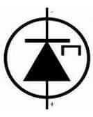
Figure 1. electrical symbol of the tunnel diode
Ⅱ Qualitative analysis of tunneling process
Both sides of the tunnel diode PN junction are degenerate semiconductors with high doping concentration. The volt-ampere characteristic curve of the diode is shown in Figure 2 below. The energy band diagram of the degenerate semiconductor PN junction can qualitatively illustrate the characteristics of the tunnel diode.

Figure 2. characteristics of the tunnel diode
Due to the high doping on both sides of the PN junction, the Fermi level enters their respective energy bands, and the uniform Fermi level is at equilibrium. The energy band of the barrier region of the tunnel diode PN junction is more serious than that of the ordinary PN junction. The thickness of the barrier region is thin, and the energy band at equilibrium is shown in Figure 2(a) below. Since the state above the Fermi level is empty and the state below the Fermi level is filled with electrons, there is no tunnel current at this time. Only under the action of an applied voltage, the Fermi energy levels of the P and N regions move, and the carriers move to form a current.
Figure 2(b) below shows the band diagram when the PN junction is reverse biased. Reverse bias moves the Fermi energy level in the P region upward relative to the Fermi energy level in the N region so that a part of the electronic states below the P region and the empty states above the N region is at the same energy level, and the electrons in the P region pass through the barrier "tunnel" crossing to the N zone, a reverse tunnel current is formed. This corresponds to point 1 in Figure 1.

Figure 3. Energy Band Diagram of Tunnel Diode
Figure 3 (c) ~ (g) is the energy band diagram when the PN junction is forward biased. As the forward bias increases, relative to the upward movement, corresponding to Figure 3(c). The following part of the electrons are at the same energy as the above part of the empty state, and the electrons in the N region pass through the tunnel to the P region to form a forward tunnel current. This corresponds to point 2 in Figure 1. The forward bias increases, compared with the upward movement, the electron state of the conduction band in the N region overlaps more with the empty state of the valence band in the P region, and the forward tunnel current increases. When the energy band overlaps the most, the number of carriers passing through the tunnel reaches the maximum value, and the forward tunnel current reaches the maximum value, which corresponds to point 3 in Fig. 2(d) and Fig. 1. The forward voltage further increases, relatively, and moves upward, but the overlap between the N-zone electronic state and the P-zone empty state gradually decreases. The number of N-zone electrons passing through the tunnel decreases, and the forward tunnel current decreases, corresponding to Figure 3. (E) and point 4 in Figure 1. When the forward bias increases so that the electronic state moving up to the N zone and the empty state of the P zone do not overlap, the forward tunneling current drops to the minimum value, corresponding to point 5 in Figure 3(f) and Figure 1. When the forward voltage increases further, a normal PN junction injection current appears, which increases exponentially with the applied voltage, corresponding to point 6 in Figure 3(g) and Figure 1.
It can be seen that the tunnel diode volt-ampere characteristic curve has two positive slope regions and one negative slope region. From 3 o'clock to 5 o'clock, as the positive voltage increases, the current decreases, and a negative resistance characteristic appears. Within a certain current range, voltage is a multi-valued function of current.
Ⅲ Features and applications of tunnel diodes
The main feature of the tunnel diode is its forward current-voltage characteristic with negative resistance (see figure). This negative resistance is based on the quantum mechanical tunnel effect of electrons, so the switching speed of the tunnel diode is on the order of picoseconds, and the operating frequency is as high as 100 GHz. The tunnel diode also has the characteristics of low power consumption and low noise. Tunnel diodes can be used for microwave mixing and detection (in this case, doping should be appropriately reduced and made into reverse diodes), low noise amplification, oscillation, etc. Due to its low power consumption, it is suitable for satellite microwave equipment. It can also be used in ultra-high-speed switching logic circuits, flip-flops, and storage circuits.

Figure 4. the forward current-voltage characteristic of tunnel diode
Studying the basic characteristics of tunnel diodes made of different semiconductor materials can also gain insight into the energy band structure of semiconductors and some physical issues related to quantum mechanics.
Ⅳ Tunnel effect
The tunnel effect is a quantum effect determined by the volatility of microscopic particles. It is also known as barrier penetration. Considering that the movement of a particle encounters a potential barrier higher than the energy of the particle, it is impossible for a particle to cross the barrier according to classical mechanics. According to quantum mechanics, it can be solved that in addition to the reflection at the barrier, there are also waves passing through the barrier. It shows that on the other side of the barrier, the particle has a certain probability that the particle penetrates the barrier.
Theoretical calculations show that for electrons with energy of several electron volts, the energy of the square barrier is also several electron volts. When the barrier width is 1 angstrom, the transmission probability of the particle reaches a few tenths; when the barrier width is 10 angstrom, The particle transmission probability has been reduced to 10^-10, which is very small. It can be seen that the tunnel effect is a quantum effect in the micro world, and it is practically impossible for a macro phenomenon to occur.
When the kinetic energy of a particle moving on one side of the barrier is less than the height of the barrier, it is impossible for the particle to pass through the barrier according to classical mechanics. For microscopic particles, quantum mechanics proves that it still has a certain probability to pass through the potential barrier, which is also true in reality. This phenomenon is called the tunneling effect. For harmonic oscillators, according to classical mechanics, the potential energy determined by the internuclear distance can never exceed the total energy. Quantum mechanics proves that this inter-nuclear distance still has a certain probability. This phenomenon is also a tunnel effect. The tunnel effect is the basis for understanding many natural phenomena.
A thin insulating layer is sandwiched between two metal conductors to form an electron tunnel junction. Experiments have found that electrons can pass through the tunnel junction, that is, electrons can pass through the insulating layer, which is the tunneling effect. The potential energy of electrons in metals is lower than that in the air or insulating layers. Therefore, the effect of the electron tunnel junction on the electrons can be represented by a potential barrier. In order to simplify the calculation, the potential barrier is simplified into a one-dimensional square potential barrier.
The so-called tunneling effect refers to a very thin insulating layer (about a few nm (10-9m) thick, such as an oxide film) sandwiched between two pieces of metal. When potential energy is applied at both ends to form a potential barrier V, under the condition of E<V, some particles of kinetic energy E can pass through the barrier V from one side of the insulating layer to a physical phenomenon on the other side.
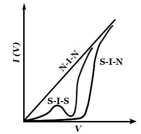
Figure 5. IV characteristic curve of a tunnel junction
The reason for the tunneling effect is the volatility of electrons. According to the principle of quantum mechanics, at low speed, the wavelength of an electron with energy (kinetic energy) E
hλ=-√2mE
(Among them, h——Planck's constant 24x; m——electron mass; E——electron kinetic energy), before the barrier V: if E>V, when it enters the barrier V region, change the wavelength to
hλ’=-√2m(E-V)
If E<V, although a certain wavelength fluctuation cannot be formed, electrons can still enter a certain depth of the V zone. When the barrier zone is very narrow, even if the kinetic energy E is smaller than the barrier V, some electrons will penetrate the V zone while the kinetic energy E remains unchanged. In other words, when E<V, the electron incident barrier must have reflected electron waves, and also transmitted waves.
Related Articles:
 UTMEL
UTMEL
We are the professional distributor of electronic components, providing a large variety of products to save you a lot of time, effort, and cost with our efficient self-customized service. careful order preparation fast delivery service
What is a tunnel diode used for?
The tunnel diode is used in many microwave applications where it can be used in oscillators and amplifiers. The tunnel diode is a type of microwave semiconductor diode that can be used in oscillators and also amplifiers.
What is tunnel diode explain?
The tunnel diode is a highly conductive, heavily doped PN-junction diode in which the current induces because of the tunnelling. The tunnelling is the phenomenon of conduction in the semiconductor material in which the charge carrier punches the barrier instead of climbing through it.
What is the difference between Zener diode and tunnel diode?
Zener diode is a heavily doped p-n junction diode. It is biased in the reverse direction. Tunnel diode is a p-n junction diode. It is operable at very high frequency.
How do zener diodes work?
The Zener diode operates just like the normal diode when in the forward-bias mode, and has a turn-on voltage of between 0.3 and 0.7 V. ... As the reverse voltage increases to the predetermined breakdown voltage (Vz), a current starts flowing through the diode.
Why Zener diode is highly doped?
Zener diode is a heavily doped p-n junction diode. It is biased in the reverse direction. ... But while in reverse bias their junction potential is increased. So that means when the voltage crosses 6V then the diode is in Reverse breakdown and hence the current through the diode increases rapidly.
 All You Need to Know About Rectifier CircuitUTMEL24 April 202517548
All You Need to Know About Rectifier Circuit
Read More 15 Key Elements of Diode SelectionUTMEL26 November 202118860
Hello everyone, I am Rose. Welcome back to the new post today. Diodes are one of the most common components in our circuit boards. So, what factors should be considered when selecting models?
Read More What is a PIN Diode?UTMEL04 February 202110150
While diodes with a simple PN junction are by far the most common type of diode in operation, in a variety of applications, other forms of diode may be used. The PIN diode is one type that is used for a number of circuits. In a variety of places, this diode type is used. For RF switching, the PIN diode is very fine, and the PIN structure in photodiodes is very useful as well.
Read More Microwave Diode: Introduction and TypesUTMEL07 January 202125948
Microwave diodes are diodes that work in the microwave frequency band. It is a solid-state microwave device. Microwave band usually refers to the frequency from 300 MHz to 3000 GHz. After the discovery of the point contact diode effect at the end of the 19th century, microwave diodes such as PIN diodes, varactor diodes, and Schottky diode tubes appeared one after another. Microwave diodes have the advantages of small size and high reliability, and are used in microwave oscillation, amplification, frequency conversion, switching, phase shifting and modulation.
Read More What Determines the Maximum Operating Frequency of a Diode?UTMEL29 June 202212886
Hello, wish you a wonderful day. In this essay, we first pose the following query: what determines the diode's maximum operating frequency? In regards to the solution, the first thing we need to understand is that the junction capacitance and the reverse recovery time of the diode are two distinct concepts. The charging and discharging times of the junction capacitance cannot match the reverse recovery time. You say that, why? Let's start by taking a look at these facts.
Read More
Subscribe to Utmel !
![MMZ1608R102ATA00]() MMZ1608R102ATA00
MMZ1608R102ATA00TDK Corporation
![MMZ1608B121CTAH0]() MMZ1608B121CTAH0
MMZ1608B121CTAH0TDK Corporation
![NFM41PC155B1H3L]() NFM41PC155B1H3L
NFM41PC155B1H3LMurata Electronics
![NFM3DCC223R1H3L]() NFM3DCC223R1H3L
NFM3DCC223R1H3LMurata Electronics
![NFM21PC225B0J3D]() NFM21PC225B0J3D
NFM21PC225B0J3DMurata Electronics
![BLM18KG700TN1D]() BLM18KG700TN1D
BLM18KG700TN1DMurata Electronics
![MPZ1608S331ATA00]() MPZ1608S331ATA00
MPZ1608S331ATA00TDK Corporation
![BLM18BB600SN1D]() BLM18BB600SN1D
BLM18BB600SN1DMurata Electronics
![BLM21BB221SN1D]() BLM21BB221SN1D
BLM21BB221SN1DMurata Electronics
![BLM15BB750SN1D]() BLM15BB750SN1D
BLM15BB750SN1DMurata Electronics


