
 Product
 Brand
Brand Articles
 Tools
Tools
What is a PIN Diode?
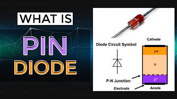
What is PIN Diode | Working of Pin Diode
Catalog
Ⅰ Definition
The PIN diode was first used as a low-frequency, high-power rectifier in 1952. In a variety of microwave applications, it was also used, but it took until around 1960 before its use in this application became more widespread. The PIN diode is further used as a photo-detector (photodetector or photo-diode) where its form is especially suited to light absorption.
The diode in which the high resistivity intrinsic layer is sandwiched between the semiconductor material P and N region, such a type of diode, is known as the PIN diode. The broad electric field between the P and N-region provides the high resistive layer of the intrinsic region. The electrical field is caused by the passage of electrons and holes. The electric field's path is from n-region to p-region.
The high electric field creates pairs of large electron holes because of which even minor signals are interpreted by the diode. The PIN diode is a kind of photodetector that is used to turn light energy into electricity.
The distance between them is expanded by the intrinsic layer between the P and N-type regions. The region's diameter is inversely proportional to its capacitance. If their capacitance decreases as the separation between the area of P and N increases. This diode function increases the reaction time and makes the diode ideal for operations such as microwave applications.
Ⅱ Structure of PIN Diode
The diode consists of the P-region and the N-region, separated by the material of the intrinsic semiconductor. The hole is the main charge carrier in the P-region, while the electron is the major charge carrier in the n-region. There is no free carrier of the intrinsic field. Between n and the p-type zone, it acts as an insulator. The i-region has a high resistance that obstructs electron flow from going through it.
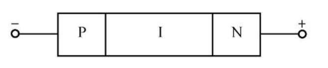
PIN Diode
The PIN diode's symbolic representation as seen in the figure below. The two terminal terminals of the PIN diode are the anode and the cathode. The anode is the positive terminal, and its negative terminals are represented by the cathode.

PIN Diode Symbol
The name of the PIN diode comes from the fact that it has three primary layers. The PIN diode has three layers, rather than only having a P type and a N-type layer:
*P-type layer
*Intrinsic layer
*N-type layer
In contrast to a standard PN junction diode, the intrinsic layer of the PIN diode is the one that offers the change in properties. The intrinsic region consists of an undoped or nearly undoped semiconductor, which is very small in most PIN diodes - in the range of 10 to 200 microns.
It is possible to use two major structures, but the one referred to as a planar structure is seen in the diagram. The intrinsic layer is seen in the diagram to be much larger than if it were drawn to proportion. This has been done to help explain the overall PIN diode structure.
PIN diodes are usually manufactured from silicon, and this was the semiconductor material used primarily before gallium arsenide began to be used in the 1980s.
Ⅲ Working of PIN Diode
The function of the PIN diode is identical to that of the regular diode. When the diode is impartial, their charge carrier can scatter. The term diffusion suggests that the depletion area's charge carriers want to travel to their region. The diffusion mechanism continues until the charges in the depletion area become balanced.
Let the N and I-layer establish the region of depletion. The diffusion of the hole and electron across the region causes the depletion layer throughout the NI region. The thin depletion layer causes the opposite polarity across the n-region, and the thick depletion region produces the opposite polarity across the I-region.
1.Forward Biased PIN Diode
When the diode is biased forward, the charges are constantly pumped from the P and N-region into the I-region. This lowers the diode's forward resistance, and it acts as a vector resistance.
The charge carrier that joins the i-region from the P and N-regions is not automatically integrated into the intrinsic region. In the intrinsic field, the finite amount of charge deposited reduces their resistivity.
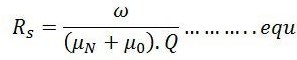
Consider Q as the volume of charge deposited in the area of depletion. The period used for the recombination of the charges is the same. Based on their recombination time, the amount of the charges deposited in the intrinsic region varies. The forward current continues to flow into the region of the I.
![]()
Where, IF – forward current
τ- recombination time
The resistance (Rs) of the propagation biased current is inversely proportional to the Q charge accumulated in the intrinsic region.
Where, w – width region
μ – electron mobility
μ0 – hole mobility
From equation (1) and (2), we get
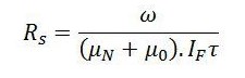
The above equation indicates that the inherent region's resistance depends on the region's distance.
2.Reversed Biased PIN Diode
The width of the depletion region increases when the reverse voltage is applied across the diode. The region's thickness increases until it is swept away by the entire I-region mobile charging carrier. The reverse voltage required is known as the swept voltage to remove the complete charge carrier from the I-region.
The diode behaves like a capacitor in reverse bias. The P and N regions act as the condenser's positive and negative plates, and the insulator between the plates is the intrinsic region.

Where, A – junction diode
w – intrinsic region thickness
The smallest frequency at which the effect begins to start is expressed as
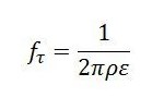
Where, ε – silicon dielectric constant
Ⅳ Characteristics of PIN diode
The PIN diode's intrinsic layer between the P-type and N-type regions allows it to have properties such as a high reverse breakdown voltage and a low capacitance frequency, and when it is forward biased, there are also other properties such as carrier storage that allow it to be used for some microwave applications.
The depletion layer is observed to become fully depleted at low levels of reverse bias. The PIN diode capacitance, if fully depleted, is independent of the degree of bias since the intrinsic layer has no net charge. The capacitance frequency, however, is usually lower than other diode types and this ensures that any leakage of RF signals through the diode is lower.
Both forms of the current carrier are inserted into the intrinsic layer where they merge while the PIN diode is forward-biased. It is this mechanism that helps the passage of the current through the sheet.
As used for high-frequency signals, the diode appears as a resistor rather than a non-linear unit, which causes no rectification or distortion, the particularly useful feature of the PIN diode happens. Its resistance is controlled by the applied DC bias. In this way, the system can be used as a powerful RF switch or variable resistor that produces much less distortion than ordinary PN junction diodes.
Ⅴ Uses and advantages of PIN diode
As a consequence of its structure demonstrating certain properties that are of special value, the PIN diode is found in a variety of fields.
High voltage rectifier: As a high voltage rectifier, the PIN diode can be used. A wider distinction between the PN and N regions is given by the intrinsic region, allowing higher reverse voltages to be tolerated.
RF switch: The PIN diode makes an RF switch perfect. The distance between them is increased by the intrinsic layer between the P and N regions. This also reduces the capacitance between them, thereby increasing the separation degree while the diode is biased backwards.
Photodetector: In the depletion region of a photodiode, when the conversion of light into current takes place, increasing the depletion region by adding the intrinsic layer increases the output by increasing the amount of light conversion.
These are three of the key PIN diode uses, although they can also be used in many other fields as well.
 UTMEL
UTMEL
We are the professional distributor of electronic components, providing a large variety of products to save you a lot of time, effort, and cost with our efficient self-customized service. careful order preparation fast delivery service
1.What is a PIN diode used for?
What is a PIN Diode? The PIN diode is one type of photodetector, used to convert the optical signal into an electrical signal. The PIN diode comprises three regions, namely P-region, I-region, and N-region. Typically, both the P and N regions are heavily doped due to they are utilized for Ohmic contacts.
2.How does a PIN diode work?
A PIN diode operates under what is known as a high-level injection. In other words, the intrinsic "i" region is flooded with charge carriers from the "p" and "n" regions. Its function can be likened to filling up a water bucket with a hole on the side. Once the water reaches the hole's level it will begin to pour out.
3.What is the full form of PIN diode?
Definition. P-I-N. Positive - Intrinsic - Negative (semiconductor)
4.For what are the PIN diode used in the microwave?
The PIN diode is one of the most versatile types for RF and Microwave designers, which is why it's used in a broad array of applications from limiters to phase shifters, modulators, attenuators, and switches. Current PIN diodes are made of gallium arsenide as well.
5.Why Zener diode is preferred over PIN diodes?
The PN junction diode is used for rectification purposes because it allows the current to flow only in one direction. The Zener diode is used as a voltage regulator in the electronic circuit because it provides the constant voltage from the supply to the load whose voltage vary over sufficient range.
 All You Need to Know About Rectifier CircuitUTMEL24 April 202517548
All You Need to Know About Rectifier Circuit
Read More 15 Key Elements of Diode SelectionUTMEL26 November 202118860
Hello everyone, I am Rose. Welcome back to the new post today. Diodes are one of the most common components in our circuit boards. So, what factors should be considered when selecting models?
Read More What is a PIN Diode?UTMEL04 February 202110151
While diodes with a simple PN junction are by far the most common type of diode in operation, in a variety of applications, other forms of diode may be used. The PIN diode is one type that is used for a number of circuits. In a variety of places, this diode type is used. For RF switching, the PIN diode is very fine, and the PIN structure in photodiodes is very useful as well.
Read More Microwave Diode: Introduction and TypesUTMEL07 January 202125948
Microwave diodes are diodes that work in the microwave frequency band. It is a solid-state microwave device. Microwave band usually refers to the frequency from 300 MHz to 3000 GHz. After the discovery of the point contact diode effect at the end of the 19th century, microwave diodes such as PIN diodes, varactor diodes, and Schottky diode tubes appeared one after another. Microwave diodes have the advantages of small size and high reliability, and are used in microwave oscillation, amplification, frequency conversion, switching, phase shifting and modulation.
Read More What Determines the Maximum Operating Frequency of a Diode?UTMEL29 June 202212886
Hello, wish you a wonderful day. In this essay, we first pose the following query: what determines the diode's maximum operating frequency? In regards to the solution, the first thing we need to understand is that the junction capacitance and the reverse recovery time of the diode are two distinct concepts. The charging and discharging times of the junction capacitance cannot match the reverse recovery time. You say that, why? Let's start by taking a look at these facts.
Read More
Subscribe to Utmel !
![MMZ1608R102ATA00]() MMZ1608R102ATA00
MMZ1608R102ATA00TDK Corporation
![MMZ1608B121CTAH0]() MMZ1608B121CTAH0
MMZ1608B121CTAH0TDK Corporation
![NFM41PC155B1H3L]() NFM41PC155B1H3L
NFM41PC155B1H3LMurata Electronics
![NFM3DCC223R1H3L]() NFM3DCC223R1H3L
NFM3DCC223R1H3LMurata Electronics
![NFM21PC225B0J3D]() NFM21PC225B0J3D
NFM21PC225B0J3DMurata Electronics
![BLM18KG700TN1D]() BLM18KG700TN1D
BLM18KG700TN1DMurata Electronics
![MPZ1608S331ATA00]() MPZ1608S331ATA00
MPZ1608S331ATA00TDK Corporation
![BLM18BB600SN1D]() BLM18BB600SN1D
BLM18BB600SN1DMurata Electronics
![BLM21BB221SN1D]() BLM21BB221SN1D
BLM21BB221SN1DMurata Electronics
![BLM15BB750SN1D]() BLM15BB750SN1D
BLM15BB750SN1DMurata Electronics


