15 Key Elements of Diode Selection

How to Select a Diode?? | TVS diode Selection | What is TVS Diode?
1. Forward conduction pressure drop
Voltage drop: Voltage drop, or voltage drop for short, is the change in the diode's potential (potential) relative to the same reference point after current flows through the load.
Turn-on voltage drop: When the diode begins to turn on, this voltage is the matching voltage.
Forward characteristics: When a forward voltage is given to the diode, the forward voltage is very low at the start of the forward characteristic, and the forward current is nearly nil because the forward voltage is insufficient to overcome the blocking effect of the electric field in the PN junction. The diode conducts forward when the forward voltage is big enough to overcome the electric field of the PN junction, and the current grows rapidly as the voltage rises.
Reverse characteristics: The current through the diode is a reverse current created by the drifting movement of minority carriers when the applied reverse voltage does not exceed a specified range. The diode is in an off state since the reverse current is so minimal. The diode reverses breakdown after the reverse voltage rises to a particular level.

The link between conduction current and forward conduction voltage drop
The internal electric field area narrows when a forward bias voltage is provided to both ends of the diode, allowing a higher forward diffusion current to pass through the PN junction. The diode can only switch on when the forward voltage exceeds a particular level (known as the "threshold voltage"; the germanium tube is about 0.2V, while the silicon tube is about 0.6V). Is the diode's conduction voltage drop, however, constant? What link does it have with the forward diffusion current? The SM360A diode's conduction current and conduction at room temperature as measured by the test circuit depicted in Figure 1 below. The voltage drop relationship test can yield the curve relationship displayed in Figure 2: The floating voltage difference is 0.2V, and the forward conduction voltage drop is proportional to the conduction current. Although the voltage difference between the light-load conduction current and the rated conduction current is just 0.2V, it affects not only the efficiency but also the temperature rise of the power diode, so try to choose the conduction voltage drop if the price conditions allow. A diode that has a tiny rated operating current that is double the real current.

Diode conduction voltage drop test circuit
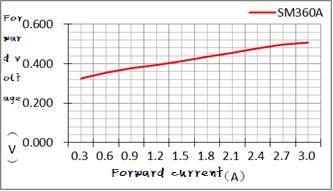
The relationship between on-voltage drop and on-current
The influence of high and low-temperature conditions on electronic components is the main hurdle to stable product functioning in our product development process. The diode is no exception to the fact that ambient temperature has a significant impact on most electrical components. The relationship curve of the measured data sheet 1 of SM360A and Figure 3 can be known in high and low temperature environments: the diode's conduction voltage drop. The ambient temperature has an inverse relationship with it. Although the conduction voltage drop is greatest at -45°C, it has no effect on the diode's stability; nonetheless, when the ambient temperature is 75°C and the case temperature exceeds the 125°C mentioned in the data sheet, the diode must be derated for operation at 75°C. One of the reasons why the switching power supply must be derated for operation at a given high temperature point is because of this.
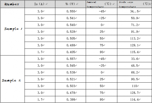
Test data of conduction voltage drop and conduction current
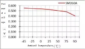
The relationship between the conduction pressure drop and the ambient temperature
2. Rated current, maximum forward current IF
The average current value estimated based on the operational temperature rise during the long-term operation of the diode is referred to as the rated current IF. The present maximum power rectifier diode's IF value can reach 1000A.

Its value is connected to the PN junction area and external heat dissipation circumstances, and it relates to the highest forward average current value that the diode is allowed to pass through for a long period continuously. Because the current traveling through the tube heats up the die, which raises the temperature. The die will overheat and be damaged if the temperature exceeds the permitted limit (approximately 141 for silicon tubes and about 90 for germanium tubes). As a result, during usage, do not exceed the diode's maximum rectified current value under the specified heat dissipation circumstances. The ubiquitous IN4001-4007 germanium diodes, for example, have a rated forward operating current of 1A.
3. Maximum average rectified current Io
Maximum average rectified current IO: The maximum value of the average rectified current flowing through the load resistance in a half-wave rectifier circuit. When converting the design, this is a critical value.
4. Maximum surge current IFSM
The operation is experiencing an excessive amount of forwarding current. It is an instantaneous current, not a regular current. This is a significant amount of money.
5. Maximum reverse peak voltage VRM
Even if there is no reverse current, the diode will be broken sooner or later if the reverse voltage is repeatedly increased. The reverse voltage that can be applied is a series of forwarding and reverse voltages that are applied repeatedly. The maximum value of the AC voltage is a defined critical factor since it is applied to the rectifier. The maximum reverse peak voltage, or VRM, is the highest reverse voltage that can be applied without causing a breakdown. The maximum VRM value currently available is several thousand volts.
6. Maximum reverse voltage VR
The highest reverse peak voltage indicated above is the peak voltage that is repeatedly applied, and VR is the amount of continuous DC voltage application. The maximum DC reverse voltage is critical in defining the allowed value and upper limit for DC current.
7. Maximum operating frequency fM
When the working frequency of a PN junction surpasses a specific value, its unidirectional conductivity deteriorates due to the presence of the junction capacitance. The fM of a point contact diode is higher, exceeding 100MHz; the fM of a rectifier diode is lower, typically not exceeding a few thousand Hz.
8. Reverse recovery time Trr
The optimal circumstance for the diode to work is for the current to be turned off instantly when the forward voltage shifts from forward to reverse voltage. In fact, there is usually some lag time. The reverse recovery time is the quantity that determines the current cut-off delay.

9. Maximum power P
The diode absorbs heat and raises its temperature as current travels through it. The maximum power P is the highest power value. Specifically, the current flowing multiplies the voltage across the loading diode. For Zener diodes and variable resistance diodes, this limit parameter is especially essential.
10. Reverse saturation leakage current IR
When a reverse voltage is applied across a diode, the current flowing through it is called reverse current. The current is proportional to the temperature and semiconductor material. The IR of the silicon tube is nA (10-9A) at ambient temperature, while the IR of the germanium tube is mA. (10-6A).
11. Derating (junction temperature derating)
Derating can help extend the life of a product and increase its reliability. The lowest derating junction temperature data for tubes with different rated junction temperatures are listed below, based on the idea that the temperature is dropped by 10°C and the service life doubles.
| Table 1 Diode Derating | ||||
| Rated valueTjM | 125℃ | 150℃ | 175℃ | 200℃ |
| TjM that can be used after derating | 110℃ | 135℃ | 160℃ | 185℃ |
12. Safety regulations
The power device should be the key consideration during the selection stage, as well as if the device has passed the safety certification. UL (North America), CSA (Canada), TUV (Germany), VDE, and other types of safety certification are generally recognized by many countries.
13. Reliability design
Correctly pick the device and the circuit design, mechanical design, and thermal design that surrounds it to manage the device's operating conditions throughout the entire machine, avoid various inappropriate stresses or operations from destroying the device, and maximize the device's inherent reliability.
14. Tolerance design
The permissible range of device characteristics (including manufacturing tolerance, temperature drift, and time drift) should be relaxed when designing a single board to ensure that the single board can function normally when the device parameters shift within a given range.
15. Prohibition of optional packaging
The use of an axially inserted diode package is prohibited, as is the use of an open-junction diode.
OPEN JUNCTION's wafer diffusion method is known as O/J. The wafer is then split into crystal grains once it has been diffused. The crystal grains' edges are jagged, and the electrical characteristics are insecure. The edges must be washed with a mixed acid (the primary component is hydrofluoric acid), then wrapped in silica gel and encapsulated molding; however, the reliability is poor.
Glassivation passivation parts, or GPP for short, is the generic word for glass passivation devices. This product is based on existing standard silicon rectifier diffuser diffusers that burn a layer of glass around the P/N junction of the divided die. Glass and monocrystalline silicon have strong bonding properties, allowing the P/N junction to be optimally insulated from the external environment, improving the device's stability and dependability.

The heat dissipation of O/J is not as good as that of GPP, and the two have fundamentally different basic structures: Pickled O/J chips must be soldered with copper sheets and wrapped in silica gel. GPP chip rectifier bridge has a greater internal structure than GPP. It is directly welded to the copper connecting piece of the rectifier bridge, eliminating the stages of pickling and applying silica gel. The internal structure of the chip is much smaller than that of O/J chips. It leads to intuitive and habitual misperceptions.
A comprehensive evaluation of GPP chip and OJ chip:
1. The GPP chip completes glass passivation at the wafer stage and can do VR probe testing, whereas the OJ chip can only test VR after the product has been assembled.
2. VRM is a 1000V GPP chip that is grooved and passivated from the P+ surface, and the mesa has a negative bevel structure (the surface electric field strength is higher than that in the body), whereas the OJ chip's cutting has no bevel.
3. Unlike the GPRC chip, which applies glass passivation to the entire section, the GPP chip distributes glass passivation in the pn junction area, whilst the OJ chip applies silicone rubber protection to the entire section.
4. Mechanical cutting leaves a cutting damage layer on the GPP chip, whereas chemical etching may erase the cutting damage layer on the OJ chip.
5. The GPP chip is passivated with a unique high-temperature molten inorganic glass layer, which improves Tjm and HTIR stability over silicone-protected OJ products.
6. Miniaturization, thinness, and LLP packaging are ideal for GPP chips, whereas lead-out packaging is ideal for OJ chips.
The difference in the production process:
(1) The soldering, pickling, passivation, whitening, curing, and baking processes are all required for the OJ chip, and its electrical qualities (reverse voltage) are intimately related to the packing and pickling processes. Plug-in packaging is the most common type of packaging.
(2) In addition, the chip manufacturing process at GPP includes pickling and passivation. The chip determines its electrical properties directly, and the patch type is the most frequent sealing form.
1. What parameters are mainly considered when choosing a diode?
1. Maximum rectified current IF
2. The highest reverse working voltage Udrm
3. Reverse current Idrm
4. Dynamic resistance Rd
5. Maximum operating frequency Fm
6. Voltage temperature coefficient αuz
2. Which two main parameters should be considered when choosing a diode?
Mainly consider the maximum reverse breakdown voltage Ubrceo and the maximum rectified current Idm.
3. How to choose Schottky diodes?
Choose the appropriate forward current and reverse withstand voltage (should be greater than the application value). For high-frequency current rectification, the general load withstand voltage is 2 times greater than the actual voltage (for example: 10V Schottky for 5V voltage). Inductive load Optional 3--5 times. The minimum current margin is 20%, (8A current chooses 10A Schottky) generally, the margin is 50% or more.
 All You Need to Know About Rectifier CircuitUTMEL24 April 202517110
All You Need to Know About Rectifier Circuit
Read More 15 Key Elements of Diode SelectionUTMEL26 November 202118624
Hello everyone, I am Rose. Welcome back to the new post today. Diodes are one of the most common components in our circuit boards. So, what factors should be considered when selecting models?
Read More What is a PIN Diode?UTMEL04 February 20219825
While diodes with a simple PN junction are by far the most common type of diode in operation, in a variety of applications, other forms of diode may be used. The PIN diode is one type that is used for a number of circuits. In a variety of places, this diode type is used. For RF switching, the PIN diode is very fine, and the PIN structure in photodiodes is very useful as well.
Read More Microwave Diode: Introduction and TypesUTMEL07 January 202125029
Microwave diodes are diodes that work in the microwave frequency band. It is a solid-state microwave device. Microwave band usually refers to the frequency from 300 MHz to 3000 GHz. After the discovery of the point contact diode effect at the end of the 19th century, microwave diodes such as PIN diodes, varactor diodes, and Schottky diode tubes appeared one after another. Microwave diodes have the advantages of small size and high reliability, and are used in microwave oscillation, amplification, frequency conversion, switching, phase shifting and modulation.
Read More What Determines the Maximum Operating Frequency of a Diode?UTMEL29 June 202212537
Hello, wish you a wonderful day. In this essay, we first pose the following query: what determines the diode's maximum operating frequency? In regards to the solution, the first thing we need to understand is that the junction capacitance and the reverse recovery time of the diode are two distinct concepts. The charging and discharging times of the junction capacitance cannot match the reverse recovery time. You say that, why? Let's start by taking a look at these facts.
Read More
Subscribe to Utmel !
![BLM41PG102SH1L]() BLM41PG102SH1L
BLM41PG102SH1LMurata Electronics
![FBMH1608HM102-T]() FBMH1608HM102-T
FBMH1608HM102-TTaiyo Yuden
![BLM18BA121SN1D]() BLM18BA121SN1D
BLM18BA121SN1DMurata Electronics
![742792034]() 742792034
742792034Würth Elektronik
![FBMH1608HM101-T]() FBMH1608HM101-T
FBMH1608HM101-TTaiyo Yuden
![MH2029-221Y]() MH2029-221Y
MH2029-221YBourns Inc.
![ACF321825-102-TD01]() ACF321825-102-TD01
ACF321825-102-TD01TDK Corporation
![NFM18PC225B0J3D]() NFM18PC225B0J3D
NFM18PC225B0J3DMurata Electronics
![BK1005LM182-T]() BK1005LM182-T
BK1005LM182-TTaiyo Yuden
![742792096]() 742792096
742792096Würth Elektronik


 Product
 Brand
Brand Articles
 Tools
Tools


