Product
 Brand
Brand Articles
 Tools
Tools
Analysis of Semiconductor Wafers
Silicon Wafer Production
Table of Contents
I. Wafer Materials: The Foundation of Modern Electronics
A wafer serves as the fundamental substrate for manufacturing semiconductor devices like transistors and integrated circuits (ICs). While various substrate materials exist, including silicon (Si), germanium (Ge), gallium arsenide (GaAs), indium phosphide (InP), and gallium nitride (GaN), silicon is by far the most prevalent. Consequently, the term "wafer" typically implies a silicon wafer unless another material is specified.
Intricate circuit element structures are fabricated onto these wafers, transforming them into IC products with specific electrical functions. The journey begins with silicon, an element abundantly found in the earth's crust in the form of silica. Silica ore is refined in an electric arc furnace, chlorinated with hydrochloric acid, and then distilled to produce high-purity polycrystalline silicon, achieving purities up to 99.999999999% (eleven nines or 11N).
This high-purity material is the basic ingredient for producing semiconductor devices. Through processes like crystal pulling and slicing, it is transformed into wafers. A series of complex manufacturing steps then create minuscule circuit structures on the wafer. Finally, the wafer is diced into individual chips, which are packaged, tested, and integrated into a vast array of electronic equipment. After more than 70 years of technological evolution, the wafer material industry is dominated by silicon, complemented by a growing ecosystem of new semiconductor materials for specialized applications.
In the 1950s, germanium (Ge) was the pioneering semiconductor material, first used in discrete devices. The invention of the integrated circuit marked a monumental leap for the industry. In July 1958, Jack Kilby of Texas Instruments successfully demonstrated the first IC, which was fabricated on a piece of germanium. [1]
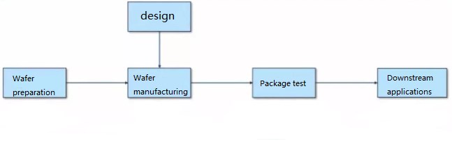
The semiconductor industry chain process, from raw materials to final application.
However, germanium-based devices exhibited limitations in high-temperature performance and radiation resistance. By the late 1960s, they were largely superseded by devices made from silicon (Si). Silicon offered significant advantages: its reserves are vast, its purification and crystallization processes are mature, and the silicon dioxide (SiO₂) layer formed during oxidation serves as an excellent insulator, dramatically improving device stability and reliability. As a result, silicon became the cornerstone of the semiconductor industry. Today, more than 95% of all semiconductor devices and over 99% of integrated circuits globally are built on a silicon substrate.
The market data underscores silicon's dominance. In 2024, the global silicon wafer market revenue was approximately **$11.5 billion**, a slight decrease from previous years but still representing the lion's share of the substrate market. [2] In contrast, the combined market for compound semiconductor substrates like GaAs, GaN, and SiC, while growing rapidly, remains significantly smaller. The central role of silicon in electronics is not expected to diminish in the foreseeable future. Nevertheless, the inherent physical properties of Si material limit its effectiveness in certain optoelectronic, high-frequency, and high-power applications, creating opportunities for alternative materials.
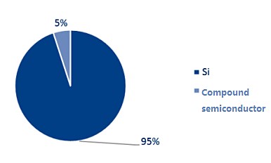
Silicon overwhelmingly dominates the semiconductor material market share.
Beginning in the 1990s, second-generation semiconductor materials, represented by gallium arsenide (GaAs) and indium phosphide (InP), gained prominence. These materials are well-suited for creating high-speed, high-frequency, high-power, and light-emitting electronic devices. They became essential for applications in satellite communications, mobile networks, optical communications, and GPS navigation. However, the scarcity, high cost, and toxicity of GaAs and InP materials (InP is a suspected carcinogen) have constrained their broader application.
The third generation of semiconductor materials, primarily silicon carbide (SiC) and gallium nitride (GaN), are known as wide-bandgap semiconductors because their bandgap (Eg) exceeds 2.3 electron volts (eV). Compared to their predecessors, these materials offer superior thermal conductivity, higher breakdown field strength, greater electron drift velocity, and higher bonding energy. These properties make them ideal for new applications demanding operation under harsh conditions, such as high temperatures, high voltages, and high frequencies. They are critical for advancements in national defense, aerospace, oil exploration, and next-generation telecommunications. In strategic industries like electric vehicles, renewable energy, and 5G/6G networks, they can reduce energy losses by over 50% and decrease equipment volume by more than 75%, representing a significant technological milestone.
II. Wafer Preparation: From Polycrystal to Polished Substrate
The preparation of a wafer involves two main stages: substrate preparation and the epitaxy process. The substrate is a wafer sliced from a semiconductor single crystal. It can either be used directly in the device manufacturing process or undergo an additional step called epitaxy, where a new single-crystal layer is grown on its surface. This epitaxial layer can be of the same material as the substrate (homoepitaxy) or a different material (heteroepitaxy), providing greater flexibility in device design.
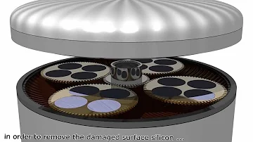
The journey to a substrate begins with purifying polycrystalline materials, adding dopants for desired electrical properties, and then "pulling" a large single crystal from the molten material. Using silicon as an example, silica sand is first refined to metallurgical-grade silicon (~98% purity). This is further purified to obtain electronic-grade polycrystalline silicon with a purity exceeding 99.9999999% (9N or higher). A single-crystal silicon rod, or ingot, is then grown from this material using methods like the Czochralski process. This ingot is then subjected to mechanical processing, chemical treatment, and surface polishing to produce a polished wafer that meets stringent standards for thickness, crystal orientation, flatness, and surface damage. Polishing is crucial for removing any residual damage from the slicing and grinding processes, resulting in a mirror-like surface ready for device fabrication or epitaxy.
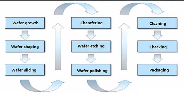
The fundamental steps involved in preparing a semiconductor substrate.
The epitaxial growth process is dominated by two primary technologies: Metal-Organic Chemical Vapor Deposition (MOCVD) and Molecular Beam Epitaxy (MBE). MOCVD is known for its faster growth rate and is generally preferred for industrial mass production. MBE, while slower, offers atomic-level precision and is better suited for complex structures like PHEMTs (Pseudomorphic High Electron Mobility Transistors) and certain antimony (Sb) based compounds. Other techniques include Hydride Vapor Phase Epitaxy (HVPE), mainly used for producing bulk GaN substrates, and Liquid Phase Epitaxy (LPE), an older technology that has been largely replaced by vapor deposition methods for silicon.
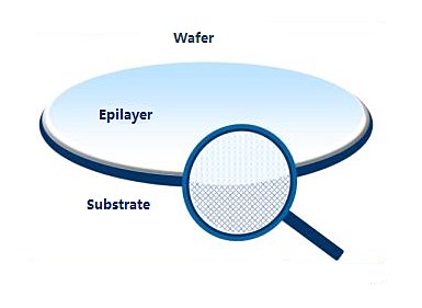
An epitaxial wafer consists of a grown single-crystal layer on a substrate.
III. Wafer Size Evolution: Scaling for Cost and Efficiency
The development of wafer technology has seen a continuous push towards larger diameters, which directly translates to lower manufacturing costs per chip. For silicon, the current industry standard and maximum size in mass production is 12 inches (300 mm). The larger surface area allows for more chips to be fabricated simultaneously, improving production efficiency. As of 2024, 12-inch wafers account for approximately 65% of global silicon wafer production capacity. The previous generation, 8-inch (200 mm) wafers, still represents a significant portion of the market at 25% capacity, primarily used for mature process technologies. While there was collaborative research into developing 18-inch (450 mm) wafers, the effort was officially halted around 2022 due to immense costs and logistical challenges, solidifying 300 mm as the leading edge for the foreseeable future. [3]
In the realm of compound semiconductors, wafer sizes are generally smaller due to the greater difficulty and cost of crystal growth. For GaAs, the mainstream substrate sizes are 4 and 6 inches. For SiC, the industry has largely transitioned from 4-inch to 6-inch wafers, with 8-inch SiC wafers now entering mass production at leading suppliers like Wolfspeed and Onsemi. [4] This transition to 8-inch SiC is a critical enabler for reducing the cost of power electronics in electric vehicles and other high-power applications. For GaN, which often relies on being grown on other substrates (like silicon or SiC), wafer sizes are determined by the underlying substrate. However, native (or self-supporting) GaN substrates are typically available in 2-inch to 4-inch diameters. A recent breakthrough by Infineon demonstrated the first 300 mm (12-inch) power GaN wafers, a development that promises to dramatically lower costs and accelerate GaN adoption. [5]
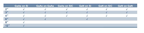
Wafer sizes vary significantly between silicon and compound semiconductors.
IV. The Silicon Wafer Market: A Stable Oligopoly
The global silicon wafer market is characterized by a high degree of concentration, with a few dominant players controlling the vast majority of the supply. This oligopolistic structure has remained remarkably stable for over two decades. Japanese manufacturers have consistently held over 50% of the market share. The top five global suppliers are:
Shin-Etsu Chemical (Japan): ~27-30% market share
SUMCO Corporation (Japan): ~26-30% market share
GlobalWafers (Taiwan): ~17% market share
Siltronic (Germany): ~13% market share
SK Siltron (South Korea): ~9% market share
Together, these five companies account for over 90% of the entire global silicon wafer market. The most significant recent change in this landscape was the acquisition of SunEdison Semiconductor by Taiwan's GlobalWafers in 2016, which elevated the company to the third-largest position. SK Siltron primarily serves the South Korean domestic market, while the other top manufacturers have a global customer base.
This market structure is sustained by high barriers to entry. Silicon wafer manufacturing requires immense capital investment, highly sophisticated technology, and a lengthy, rigorous qualification process with customers (chipmakers). Since the cost of wafers is a relatively small portion of the overall chip manufacturing cost (typically under 10%), foundries are reluctant to risk switching to unproven suppliers to save a small amount on raw materials. This dynamic protects the incumbent players and ensures the market remains stable, even as the semiconductor fabrication (fab) landscape has seen significant geographic shifts over the years.
V. Downstream Applications for Silicon Wafers: Process Nodes and Uses
The advancement in semiconductor technology follows two parallel paths: increasing wafer size to reduce cost and shrinking the process node (the size of transistors) to improve performance and density. Each generation of process technology is typically associated with a specific wafer size.
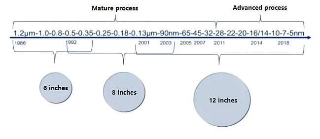
Different wafer sizes are typically used for specific process technology nodes and applications.
Today's most advanced processes, such as 3nm and 2nm nodes, are exclusively run on 12-inch wafers. These leading-edge technologies, which often employ complex transistor architectures like FinFET and Gate-All-Around (GAA), are essential for high-performance computing (HPC), artificial intelligence (AI) accelerators, and the main processors in premium smartphones. The development of 2nm process nodes is well underway, with major foundries like TSMC and Samsung targeting mass production in the 2025-2026 timeframe. [6]
The distribution of wafer demand is diverse. In 2024, memory products like DRAM and NAND Flash, along with logic chips for CPUs and GPUs, were the primary drivers of 12-inch wafer demand. Mature process nodes, typically 28nm and older, are manufactured on both 12-inch and 8-inch wafers. These nodes are cost-effective and used for a wide range of applications, including:
45nm to 90nm (12-inch): Mobile phone baseband chips, Wi-Fi, Bluetooth, GPS, and some microcontrollers (MCUs).
90nm to 0.15µm (8-inch or 12-inch): MCUs, fingerprint sensors, image sensors, and power management ICs (PMICs).
0.18µm and older (8-inch or 6-inch): Analog circuits, power devices (MOSFETs, IGBTs), and chips for smart cards and SIM cards.
The continued demand for 8-inch wafers is fueled by the explosive growth of the Internet of Things (IoT), automotive electronics, and industrial applications, which rely on these proven and cost-effective mature technologies.
VI. Compound Semiconductors: Enabling High-Performance Applications
While silicon forms the bedrock of the digital world, compound semiconductors are crucial for high-performance analog, radio frequency (RF), and photonic applications where silicon's properties fall short. The market for these materials is also highly concentrated.
1. The Supplier Landscape for Compound Semiconductors
The compound semiconductor substrate market is an oligopoly dominated by Japanese, American, and German firms. For GaAs substrates, the market is controlled by four major players—Sumitomo Electric (Japan), Freiberger (Germany), AXT (USA), and Sciocs (a subsidiary of Sumitomo Chemical, Japan)—who collectively hold over 90% of the market. The SiC substrate market is led by America's Wolfspeed (formerly part of Cree), which accounts for over a third of the market, followed by Germany's SiCrystal and American firms II-VI (now Coherent) and Dow Corning. For GaN substrates, three Japanese companies—Sumitomo Electric, Mitsubishi Chemical, and Sumitomo Chemical—monopolize over 85% of the market. In the epitaxial growth segment, UK-based IQE is the undisputed leader with over 60% market share, with Taiwan's Visual Photonics also holding a significant position.
The GaAs component market is dominated by a few large IDMs (Integrated Device Manufacturers).
2. Downstream Applications for Compound Semiconductors
Downstream applications for compound semiconductors are broadly divided into optical devices and electronic devices. Optical devices include LEDs, laser diodes (LDs), and photodetectors (PDs). Electronic devices include power amplifiers (PAs), low-noise amplifiers (LNAs), RF switches, and high-voltage power electronics.
GaAs is a cornerstone of the RF industry, especially for power amplifiers found in virtually every smartphone. It is also used for infrared LEDs and red laser diodes.
GaN has emerged as a key material for high-frequency, high-power applications. GaN-on-SiC is the preferred technology for 5G base station power amplifiers due to its high power density and the excellent thermal conductivity of the SiC substrate. GaN-on-Si is gaining traction for power adapters and data center power supplies due to its cost advantages.
SiC is rapidly becoming the material of choice for high-voltage power electronics, particularly in electric vehicles (EVs) for inverters, on-board chargers, and DC-DC converters. Its ability to handle higher voltages and temperatures more efficiently than silicon leads to significant improvements in EV range and charging speed.
InP is critical for high-performance fiber optic communication systems, enabling the high-speed data transmission that powers the internet.
VCSELs (Vertical-Cavity Surface-Emitting Lasers), often made from GaAs, are essential for 3D sensing applications like facial recognition in smartphones and LiDAR systems for autonomous vehicles.
VII. 2025 Update: Recent Trends and Future Outlook
Since this article was originally published in 2020, the semiconductor industry has experienced significant shifts driven by technological innovation, geopolitical factors, and evolving market demands. Here is a summary of the most important updates as of 2025.
Market Dynamics: The global semiconductor market saw a downturn in 2023 followed by a recovery starting in late 2024, driven heavily by the demand for AI accelerators and High-Bandwidth Memory (HBM). The overall semiconductor market reached approximately $627 billion in 2024. While silicon wafer shipments saw a slight decline in 2024 to $11.5 billion, the market is projected to rebound, with forecasts predicting the silicon wafer market to exceed $17 billion by 2030. [2]
Advanced Process Nodes: The race to smaller process nodes has continued unabated. While 5nm was considered leading-edge in 2020, foundries are now in volume production of 3nm chips. The next frontier is 2nm, which will feature the transition from FinFET to Gate-All-Around (GAA) transistor architecture, promising further improvements in performance and power efficiency. Major players like TSMC, Samsung, and Intel are all on track for 2nm production in the 2025-2026 timeframe. [6]
Wafer Size Developments: The industry has solidified its stance on wafer sizes. The much-discussed transition to 450mm (18-inch) wafers has been officially shelved, with the industry consensus focusing on maximizing the efficiency of existing 300mm fabs. In the compound semiconductor space, the transition to 8-inch SiC wafers is now in full swing, which is crucial for meeting the surging demand from the electric vehicle market. Furthermore, a major breakthrough was achieved with the demonstration of 300mm GaN-on-Si wafers, paving the way for cost-effective, high-volume production of GaN power devices. [5]
Geopolitical Influence: Geopolitical tensions and national industrial policies, such as the US CHIPS Act and similar initiatives in Europe and Asia, are reshaping the global supply chain. There is a strong push to diversify semiconductor manufacturing geographically, leading to significant new fab investments in North America and Europe. This trend aims to reduce reliance on East Asia, which has historically dominated chip production.
Emerging Applications: The demand for specialized chips continues to grow. AI and machine learning are the single largest drivers of innovation, requiring massive computational power. The growth of electric and autonomous vehicles is fueling demand for a wide range of semiconductors, from powerful SiC power modules to sophisticated sensor and processing chips. The expansion of 5G/6G networks and the proliferation of IoT and edge computing devices also continue to drive strong demand for both leading-edge and mature process nodes.
References
Computer History Museum. (1958). "All Semiconductor 'Solid Circuit' is Demonstrated." Retrieved from https://www.computerhistory.org/siliconengine/all-semiconductor-solid-circuit-is-demonstrated/
SEMI. (2025, February 13). "Worldwide Silicon Wafer Shipments and Revenue Start Recovery in Late 2024, SEMI Reports." Retrieved from https://www.semi.org/en/semi-press-release/worldwide-silicon-wafer-shipments-and-revenue-start-recovery-in-late-2024-semi-reports
The Register. (2022, August 8). "How TSMC killed 450mm wafers for fear of Intel, Samsung." Retrieved from https://www.theregister.com/2022/08/08/how_tsmc_killed_450mm_wafers/
TrendForce. (2024, October 14). "How Many 8-inch Silicon Carbide Wafer Fabs are There Worldwide?" Retrieved from https://www.trendforce.com/news/2024/10/14/news-how-many-8-inch-silicon-carbide-wafer-fabs-are-there-worldwide/
Infineon Technologies. (2025, July 2). "Infineon advances on 300-millimeter GaN manufacturing." Retrieved from https://www.infineon.com/press-release/2025/INFXX202507-122
TSMC. "2nm Technology." Retrieved from https://www.tsmc.com/english/dedicatedFoundry/technology/logic/l_2nm
 UTMEL
UTMEL
We are the professional distributor of electronic components, providing a large variety of products to save you a lot of time, effort, and cost with our efficient self-customized service. careful order preparation fast delivery service
What are semiconductor wafers used for?
In electronics, a wafer (also called a slice or substrate) is a thin slice of semiconductor, such as crystalline silicon (c-Si), used for the fabrication of integrated circuits and, in photovoltaics, to manufacture solar cells. The wafer serves as the substrate for microelectronic devices built in and upon the wafer.
What are semiconductor wafers made of?
Wafers are made up of very pure single crystal material. In the czochralski process a cylindrical ingot of highly pure monocrystalline semiconductor like silicon or germanium is made by pulling of a seed crystal from a melt.
How do you make a wafer semiconductor?
To make wafers, silicon is purified, melted, and cooled to form an ingot, which is then sliced into discs called wafers. Chips are built simultaneously in a grid formation on the wafer surface in a fabrication facility or “fab.”
How much do wafers cost?
The retail price of a basic one-inch silicon wafer without any special features is about $21 when purchased in quantity. A bulk purchase of similar 6-inch silicon wafers costs about $125 per unit, which is about 6 times the price of the one-inch wafer.
How many types of wafers are there?
There are two types of Doped Silicon Wafers, the P-type and the N-type. The P-type wafer is doped with boron. It is commonly used for lithography or making printed circuits.
 Modeling Wide Band-Gap Semiconductors for Enhanced PerformanceRakesh Kumar, Ph.D.31 January 20243567
The article delves into the challenges faced by silicon-based power electronic devices and highlights the potential of wide band-gap semiconductors. It also emphasizes the importance of modeling power semiconductor devices and provides insights into various models. For electrical energy conversion to be dependable and effective, power electronics and semiconductor device technologies are essential.
Read More Optimizing Energy Management with Non-Isolated DC-DC ConvertersRakesh Kumar, Ph.D.04 February 20243223
The article classifies DC-DC converters and discusses the benefits and limitations of them. It proposes a modified DC-DC converter topology that combines the Cuk and Positive Output Super Lift Luo topologies to achieve a higher voltage gain with fewer components.
Read More ‘6G Networks’ - Pioneering the Next Era of Connectivity And InnovationRakesh Kumar, Ph.D.18 March 20243570
The article provides a comprehensive overview of the evolving landscape of mobile networks, the requirements that will shape the future of mobile communication, and the innovative technologies driving the transition to 6G.
Read More Review of IoT-Based Smart Home Security Systems- Part 1Rakesh Kumar, Ph.D.28 March 20243975
The article discusses the evolution of IoT-based smart home security systems, integrating advanced technologies like Raspberry Pi, PIR sensors, and voice recognition for enhanced user experience and efficiency.
Read More Understanding Photodiodes: Working Principles and Applications - Part 2Rakesh Kumar, Ph.D.24 May 20245082
The article provides a comprehensive overview of photodiodes, focusing on their operational principles, key factors affecting their efficiency, advantages, and disadvantages, and highlights their diverse applications.
Read More
Subscribe to Utmel !
![314-POUCH]()
![AC1101]() AC1101
AC1101Molex
![A88975-000]() A88975-000
A88975-000TE Connectivity
![343648-000]() 343648-000
343648-000TE Connectivity
![FLX40-020-04]() FLX40-020-04
FLX40-020-04TE Connectivity
![7100138298]()
![7100166936]()
![7100138300]()
![7100138299]()
![7459]() 7459
7459Greenlee