
 Product
 Brand
Brand Articles
 Tools
Tools
Samsung: 3nm Yield Rate of 20%
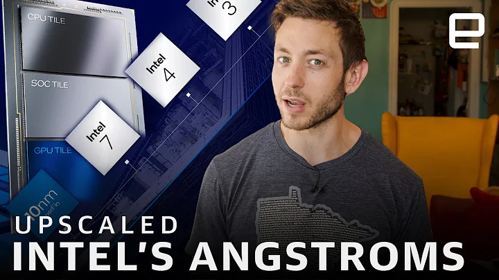
Intel has a plan to go beyond 3nm chips | Upscaled
According to foreign media Phonearena, Samsung foundry is the second-largest independent foundry in the world after the giant TSMC. In other words, in addition to manufacturing its own designs for Exynos chips, Samsung also makes chips based on designs submitted by third-party companies such as Qualcomm and other foundry customers.
The Snapdragon 865 application processor (AP) is built by TSMC using its 7nm process node. With the 5nm Snapdragon 888 chipset, Qualcomm went back to Samsung and continues to rely on the Korean foundry to produce the 4nm Snapdragon 8 Gen 1. This is the AP that currently powers high-end Android phones made by Samsung, Xiaomi, and Motorola.

Samsung Foundry Continues to Struggle with Yield Rates
But in February, it was reported that Samsung Foundry's yield at its 4nm process node was only 35%. That means only 35 percent of the die-cut from wafers will pass quality control. By comparison, TSMC achieved a 70% yield on its 4nm Snapdragon 8 Gen 1 Plus. In other words, all things being equal, TSMC manufactured twice as many chips as Samsung foundries in the same period.
This results in TSMC eventually receiving orders from Qualcomm to build its remaining Snapdragon 8 Gen 1 chipset as well as the Snapdragon 8 Gen 1 Plus SoC. We also assume that TSMC will be licensed to build the 3nm Snapdragon 8 Gen 2, even though Qualcomm will need to pay a premium to TSMC to allow the exclusive manufacturer of that chipset to build enough chips in a short period of time to make enough chips.
Although Samsung has recently said its yields have been increasing, a Business Post report says Samsung's 3nm process node yields are still well below the company's target. While Samsung Foundry's all-ring gate (GAA) transistor architecture debuted its 3nm node, putting it ahead of TSMC (which will launch its GAA architecture for its 2nm node), Samsung Foundry's yields in its early 3nm production have been in the 10 to 20 percent range.
Not only is this a very low yield that Samsung needs to improve, but it is worse than the aforementioned 35% yield that Sammy experienced in the 4nm Snapdragon 8 Gen 1.
Wccftech said that according to sources, the first "performance version" of the 3nm GAA chipset that Samsung will ship to customers starting next year could actually be the new internal Exynos chip. Samsung has reportedly been developing a new family of Exynos chips for its smartphones, but it's unclear at this stage whether they will be manufactured using the 3nm GAA process node.

TSMC and Samsung Will Soon Have New Challengers For Process Leadership
TSMC and Samsung will soon have new challenges as Intel has said it aims to take over the industry's process leadership by the end of 2024. It has also been the first to acquire a more advanced extreme ultraviolet (EUV) lithography machine.
The second-generation EUV machines are called High NA or high numerical aperture. The current EUV machine has an NA of 0.33, but the new machine has an NA of 0.55. The higher the NA, the higher the resolution of the circuit pattern etched on the wafer. This will help chip designers and foundries make new chipsets that contain even more transistors than the billions of transistors used on current integrated circuits.
It will also prevent foundries from running wafers through the EUV machine again to add additional features to the chip. small said that the higher resolution patterns produced by the second generation EUV machine will provide higher resolution will make the chip features 1.7 times smaller and the chip density 2.9 times higher.
By getting this machine first, Intel will be able to take a big step toward its goal of reclaiming process leadership from TSMC and Samsung.

Related News
1、Chip Packaging Lead Time Has Grown to 50 Weeks
2、Eight Internet of Things (IoT) Trends for 2022
3、Demand for Automotive Chips Will Surge 300%
4、Volkswagen CFO: Chip Supply Shortage Will Continue Until 2024
5、BMW CEO: The Car Chip Problem Will Not Be Solved Until 2023
6、Shenzhen: This Year Will Focus on Promoting SMIC and CR Micro 12-inch Project
 UTMEL
UTMEL
We are the professional distributor of electronic components, providing a large variety of products to save you a lot of time, effort, and cost with our efficient self-customized service. careful order preparation fast delivery service
 UTMEL 2024 Annual gala: Igniting Passion, Renewing BrillianceUTMEL18 January 20244862
As the year comes to an end and the warm sun rises, Utmel Electronics celebrates its 6th anniversary.
Read More Electronic Components Distributor Utmel to Showcase at 2024 IPC APEX EXPOUTMEL10 April 20245858
Utmel, a leading electronic components distributor, is set to make its appearance at the 2024 IPC APEX EXPO.
Read More Electronic components distributor UTMEL to Showcase at electronica ChinaUTMEL07 June 20244441
The three-day 2024 Electronica China will be held at the Shanghai New International Expo Center from July 8th to 10th, 2024.
Read More Electronic components distributor UTMEL Stands Out at electronica china 2024UTMEL09 July 20244818
From July 8th to 10th, the three-day electronica china 2024 kicked off grandly at the Shanghai New International Expo Center.
Read More A Combo for Innovation: Open Source and CrowdfundingUTMEL15 November 20195387
Open source is already known as a force multiplier, a factor that makes a company's staff, financing, and resources more effective. However, in the last few years, open source has started pairing with another force multiplier—crowdfunding. Now the results of this combination are starting to emerge: the creation of small, innovative companies run by design engineers turned entrepreneurs. Although the results are just starting to appear, they include a fresh burst of product innovation and further expansion of open source into business.
Read More
Subscribe to Utmel !
![EML30US48-E]() EML30US48-E
EML30US48-EXP Power
![KWD10-1515]() KWD10-1515
KWD10-1515TDK-Lambda Americas Inc.
![YAW1012E]() YAW1012E
YAW1012ECosel USA, Inc.
![RAC03-05SC]() RAC03-05SC
RAC03-05SCRecom Power
![EML30US36-E]() EML30US36-E
EML30US36-EXP Power
![VAF505]() VAF505
VAF505Cosel USA, Inc.
![KMD15-1212]() KMD15-1212
KMD15-1212TDK-Lambda Americas Inc.
![PBK-5-24]() PBK-5-24
PBK-5-24CUI Inc.
![PFE300SA28]() PFE300SA28
PFE300SA28TDK-Lambda Americas Inc.
![VCP24US24-E]() VCP24US24-E
VCP24US24-EXP Power


