Comprehensive Introduction to Snapdragon 888

Qualcomm Snapdragon 888: Top 5 features in 5 minutes!
Catalog
| Ⅰ Introduction |
| Ⅱ Specifications |
| Ⅲ Technical indicator |
| Ⅳ Snapdragon 888 and Snapdragon 870 Comparison |
Ⅰ Introduction
Snapdragon 888 is a big upgrade for Qualcomm's Top 8 Series chipsets in terms of 5G for the first time: unlike the Snapdragon 865, it includes a fully integrated 5G modem.
Snapdragon 888 adopts the Snapdragon X60 modem announced earlier in Qualcomm, which uses a 5nm process to achieve better power efficiency. X60 modem improves 5G carrier aggregation, across millimeter-wave mmWave and frequency spectrum below 6GHz. It supports multi-SIM cards around the world, SA, NSA, and dynamic spectrum sharing. The new processor appears to enhance battery life significantly thanks to its innovative 5nm architecture and integrated modem.
In addition to 5G improvements, Qualcomm also predicts the other progress of Snapdragon 888, including the sixth-generation AI engine and the second generation of sensing hub. The engine is expected to significantly improve the AI task's performance and power economy. According to the business, AI computing capacity has surpassed 26 TOPS. In terms of gaming, Qualcomm will introduce the third-generation Snapdragon Elite Gaming and "Trike Adreno GPU performance, most substantial upgrade," which will offer 144 frames per second.
Finally, Snapdragon 888 has implemented new photography features, including the updated ISP that supports faster billion-pixel processing speed. Users may take images and films at a rate of 2.7 billion pixels per second, which means 120 frames with 12 million pixels each frame are captured every second. According to reports, it is 35 percent faster than the previous version.
Ⅱ Specifications
The Snapdragon 888 is built using Samsung's 5nm technology. 1 x 2.84GHz (ARM's newest Cortex X1 core) + 3 x 2.4GHz (Cortex A78) + 4 x 1.8GHz are used in the CPU (Cortex A55). GPU is Adreno 660. MODEM baseband is X60 5G and supports WiFi 6E and Bluetooth 5.2.
CPU
The 888 is the first chip (based on an ARM foundation architecture) to use a Cortex-X1 kernel (ARM foundation design has some high pass adjustments). Compared to A78, each X1 clock can perform 33% more of the instructions, and the SIMD hardware is doubled, and the capacity of L1 and L2 caching has doubled. The Cortex-X1 core running frequency is 2.84GHz.

Snapdragon 888 CPU new architecture diagram
Next is a cluster of three Cortex-A78 cores, the clock frequency is 2.4GHz. There are also 4 A55 cores run in 1.8GHz. The CPU is also equipped with 4MB L3 cache and 3MB system cache.
Overall, the Kryo 680 CPU promised to boost the Snapdragon 865 chipset's processor performance by 25%.
GPU
The goal of Adreno 660 is to increase rendering performance by 35% and to increase energy efficiency by 20%. It's made for games with high frame rates and low latency. The goal is to get the required game to run at 144 frames per second, but there are also certain features to improve visual quality.

Cortex-X1
NVIDIA and AMD (including PS5 and Xbox Series X GPUs) have recently developed a new approach called variable rate coloring (VRS). Shaders can now work on two or four pixels at once, rather than just one. This saves computing resources. The rendered image will not be distinguishable if the game creator is attentive. VRS has been shown to improve performance by 30%. Furthermore, it can be utilized to improve power efficiency.
Fast touch in games can reduce touch delay by up to 20%. This works at up to 120 frames per second, but it works best at 60 frames per second, thus any game can be used, even if it doesn't support higher frame rates.
10-bit HDR and sub-pixel rendering are supported by the Adreno 660. Mura compensation can also help to increase the uniformity of the OLED display ("mura" or "clouding" is nesting pixel calibration).
Camera
Snapdragon 888 is the first three ISP Snapdragon chips (the previous series chip is dual ISP). There are multiple uses for this because it can handle three distinct camera flows at the same time. For starters, it can support three 4K HDR video streams or three 28 million pixels.

3 ISP
Because each camera has its own ISP, the transition from an ultra-wide camera to a wide camera to a long-distance camera will be smoother. When the phone switches between the video streams, the prior three cameras / two ISP design causes a "jump."
The three ISPs of the SPECTRA 580 are also used for interleaving HDR because they can process short, medium, and long exposure at the same time. In addition to the 10-bit HDR photos of the HEIF image format, Snapdragon 888 can also record HDR video functions of the previous generation (Snapdragon 865 supports HDR10 + and support Dolby Video Video).
When it comes to video recording, the new chipset can capture and play 4K films at 120 frames per second, allowing it to take advantage of high-resolution 4K monitors. Returning to photography, the chip can capture 120 images at a resolution of 12 million pixels.
Connectivity
The Snapdragon 888 chipset is the first to use Qualcomm's Snapdragon X60 5G modem. Unlike the Snapdragon 865, the modem is built within the device rather than being an external chip. SUB-6 below 5G and MMWAVE millimeter waves are supported by this third-generation modem. It has a downstream speed of up to 7.5 Gbps and an upstream speed of up to 3 Gbps.
The FastConnect 6900 system, according to Qualcomm, uses Wi-Fi 6G (6GHz band AX), which can reach 3.6 Gbps and is the industry's fastest mobile Wi-Fi. The Wi-Fi 6e standard also has a shorter latency, which is important for streaming media games from a local PC (or cloud, 5G modems).
It also supports the APTX kit's dual-antenna Bluetooth 5.2 technology and high-quality, low-delay wireless audio technologies.
Ai
The sixth-generation AI engine combines the new HEXAGON 780 and GPU digital computation capabilities for a total of 26 TOPS (the computing capability of the Snapdragon S865 AI is 15 TOPS).

Fused AI accelerator
The power consumption of the second iteration of the Sensing Hub has also been reduced. It uses less than 1 mA but can accomplish more jobs than the first generation - HUB will handle 80% of simple artificial intelligence activities rather than waking up the Hexagon CPU. Simple applications, such as elevators and activity detection, as well as listening to wake-up words, fall under this category.
Safety
Snapdragon 888 can take images of the encrypted seal with tamper-proof metadata to prove the image's validity (but performed in a privacy manner).
Hypervisor is also included in the Snapdragon 888, which was previously only available on the PC's 8CX Gen 2 CPU. This is a feature that is more common on servers and desktops since it allows various operating systems to coexist on the same hardware while maintaining their independence (so if an operating system is destroyed, the security of other operating systems is unaffected).
Ⅲ Technical indicator
Cellular modem
Modem Name | QUALCOMMSNAPDRAGOX60 5G Modem - RF System |
Peak download speed | 7.5 Gbps |
Peak upload speed | 3 Gbps |
5G Spectrum | Dynamic Spectrum Sharing (DSS), millimeter wave, 6 GHz or less |
5G millimeter-wave specifications | 800 MHz bandwidth, 8 carriers, 2x2 mimo |
5G 6 GHz or less | 200 MHz Bandwidth, 4x4 MIMO |
Multi-SIM function | Worldwide 5G Multi-SIM |
Cellular technology | 5G NR, including LTE, HSPA, WCDMA, TD-SCDMA, CDMA 1x, EV-SCDMA, CDMA 1x, EV-DO, GSM / EDGE |
5G downstream speed | Up to 7.5 Gbps |
Wireless network
Wi-Fi standard | Wi-Fi 6E,Wi-Fi 6,Wi-Fi 5、802.11a / b / g,802.11n |
QUALCOMMWI-FI 6 Technical Function | MU-MIMO(Upper and Downstream),8x8Detection,160 MHzChannel Support,OFDMA(Upstream and Downstream),4K QAM,WPA3Security Support,6 GHzOperation(Wi-Fi 6E) |
Wi-Fi spectrum frequency | 2.4GHz,5GHz,6GHz |
Ⅳ Snapdragon 888 and Snapdragon 870 Comparison
1.The Snapdragon 870 processor is manufactured using a 7nm process. The 7nm technology is relatively established, and a number of successful 7nm chip mobile phones are already on the market to attract customers. The Snapdragon 888 CPU uses a 5nm manufacturing technology. 5nm is a new manufacturing technology, and the entire architecture is considerably superior to 7nm in terms of transistor density.
2.The Snapdragon 870 processor has four A77 big nuclear cores and four A55 tiny core designs, with a 3.2GHz main core frequency. The Snapdragon 870 boasts a more advanced architecture and a greater frequency of operation. The Snapdragon 888 processor features a single new super big nuclear +3 A78 large nuclear +4 A55 tiny core with a maximum frequency of 2.84GHz. Despite the lower clock speed as the Snapdragon 870, Qualcomm claims that the Snapdragon 888 provides a 25% boost in computing power over the Snapdragon 865 with the ARM Cortex-X1 CPU. It has a 25% reduction in power loss. The actual user experience is superior to the Snapdragon 865.
3.The Snapdragon 870's baseband is the Snapdragon X55, which is an external 5G baseband. Snapdragon 888 uses the Snapdragon X60 as its baseband. It has a 5G baseband built-in. The Snapdragon 888 will outperform the Snapdragon 870 in terms of structural system.
1. What are the specifications of the Snapdragon 888 processor?
CPU:

Samsung 5nm process

Eight-core CPU

1x 2.84GHz Cortex-X1 &1MB L2 cache

3x 2.42GHz A78 & 3 x512KB L2 cache

4×1.80GHz A55 & 4×128KB L2 cache

4MB L3 cache

3MB system cache

GPU: Adreno660

GPU: Frequency: 840MHz
2. How many nanometers is Snapdragon 888?
Snapdragon 888 is 5 nanometers. The Snapdragon 888 is manufactured by South Korea's Samsung and integrates a 5nm X60 baseband, which runs very fast.
3. Which is stronger, Snapdragon 888 SoC or A14?
Although the Snapdragon 888 does not seem to be on par with the peak performance of the Apple A14, the sustained performance will depend to a large extent on the power consumption of the chip. As the Snapdragon 888 integrates a new generation of 5nm process X60 5G baseband, it is ahead of the A14 external 7nm process X55 5G baseband generation.
4. What are the gaps between Snapdragon 865 and Snapdragon 888?
1) The core gap

Snapdragon 865 is equipped with 4 Cortex-A77 performance cores and 4 Cortex-A55 efficiency cores, manufactured by TSMC using its 7-nanometer manufacturing process, supplemented by Adreno650 graphics processor. Snapdragon 888 is manufactured using Samsung's 5nm process, equipped with 1x2.84GHz (ARM's latest Cortex X1 core) + 3 x 2.4GHz (Cortex A78) + 4x1.8GHz (Cortex A55) core, the overall performance of the CPU has increased by 25%, and the GPU For Adreno660, the performance has increased by as much as 35%.

2) The differences in resolution

The image processing capability of the Snapdragon 865 reaches up to 2 gigapixels per second, and it can shoot up to 8K resolution video, high dynamic range 4K video, and 960 frames per second slow-motion video. The chip also supports up to 200 million pixels. In 2021, these capabilities will be upgraded with the launch of Snapdragon 888. The chip's image processing speed is 2.7 gigapixels per second, an increase of 37%.

3) The differences in games

In terms of games, Snapdragon 865 is already the leader in mobile gaming devices, but Snapdragon 888 promises to have a 35% improvement in this area.
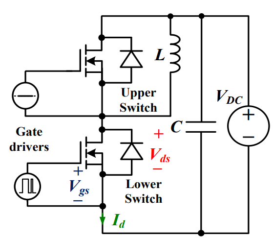
 Discovering New and Advanced Methodology for Determining the Dynamic Characterization of Wide Bandgap DevicesSaumitra Jagdale15 March 20242490
For a long era, silicon has stood out as the primary material for fabricating electronic devices due to its affordability, moderate efficiency, and performance capabilities. Despite its widespread use, silicon faces several limitations that render it unsuitable for applications involving high power and elevated temperatures. As technological advancements continue and the industry demands enhanced efficiency from devices, these limitations become increasingly vivid. In the quest for electronic devices that are more potent, efficient, and compact, wide bandgap materials are emerging as a dominant player. Their superiority over silicon in crucial aspects such as efficiency, higher junction temperatures, power density, thinner drift regions, and faster switching speeds positions them as the preferred materials for the future of power electronics.
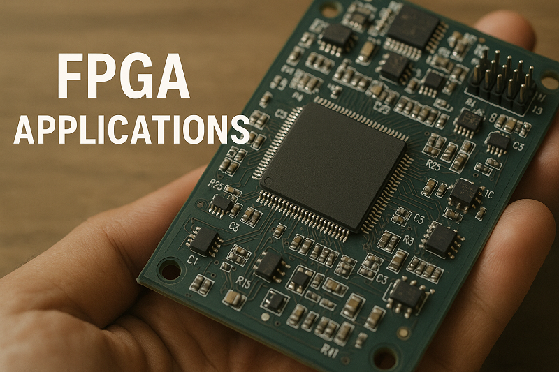
Read More A Comprehensive Guide to FPGA Development BoardsUTMEL11 September 202515417
This comprehensive guide will take you on a journey through the fascinating world of FPGA development boards. We’ll explore what they are, how they differ from microcontrollers, and most importantly, how to choose the perfect board for your needs. Whether you’re a seasoned engineer or a curious hobbyist, prepare to unlock new possibilities in hardware design and accelerate your projects. We’ll cover everything from budget-friendly options to specialized boards for image processing, delve into popular learning paths, and even provide insights into essential software like Vivado. By the end of this article, you’ll have a clear roadmap to navigate the FPGA landscape and make informed decisions for your next groundbreaking endeavor.
Read More Applications of FPGAs in Artificial Intelligence: A Comprehensive GuideUTMEL29 August 20253753
This comprehensive guide explores FPGAs as powerful AI accelerators that offer distinct advantages over traditional GPUs and CPUs. FPGAs provide reconfigurable hardware that can be customized for specific AI workloads, delivering superior energy efficiency, ultra-low latency, and deterministic performance—particularly valuable for edge AI applications. While GPUs excel at parallel processing for training, FPGAs shine in inference tasks through their adaptability and power optimization. The document covers practical implementation challenges, including development complexity and resource constraints, while highlighting solutions like High-Level Synthesis tools and vendor-specific AI development suites from Intel and AMD/Xilinx. Real-world applications span telecommunications, healthcare, autonomous vehicles, and financial services, demonstrating FPGAs' versatility in mission-critical systems requiring real-time processing and minimal power consumption.
Read More 800G Optical Transceivers: The Guide for AI Data CentersUTMEL24 December 20254317
The complete guide to 800G Optical Transceiver standards (QSFP-DD vs. OSFP). Overcome supply shortages and scale your AI data center with Utmel Electronic.
Read More Xilinx FPGAs: From Getting Started to Advanced Application DevelopmentUTMEL09 September 20254391
This guide is your comprehensive roadmap to understanding and mastering the world of Xilinx FPGA technology. From selecting your first board to deploying advanced AI applications, we'll cover everything you need to know to unlock the potential of these remarkable devices. The global FPGA market is on a significant growth trajectory, expected to expand from USD 8.37 billion in 2025 to USD 17.53 billion by 2035. This surge is fueled by the relentless demand for high-performance, adaptable computing in everything from 5G networks and data centers to autonomous vehicles and the Internet of Things (IoT). This guide will walk you through the key concepts, tools, and products in the Xilinx ecosystem, ensuring you're well-equipped to be a part of this technological revolution.
Read More
Subscribe to Utmel !
![ATAES132-MAH-ER-T]() ATAES132-MAH-ER-T
ATAES132-MAH-ER-TMicrochip Technology
![HAT1069C0S-EL-E]() HAT1069C0S-EL-E
HAT1069C0S-EL-ERenesas
![FOD4116SV]() FOD4116SV
FOD4116SVON Semiconductor
![HCS512T/SO]() HCS512T/SO
HCS512T/SOMicrochip Technology
![80HCPS1616CHMGI]() 80HCPS1616CHMGI
80HCPS1616CHMGIRenesas Electronics America Inc.
![FOD420SV]() FOD420SV
FOD420SVON Semiconductor
![EL3052]() EL3052
EL3052Everlight Electronics Co Ltd
![MCP2036T-I/SL]() MCP2036T-I/SL
MCP2036T-I/SLMicrochip Technology
![HCS370T-I/SL]() HCS370T-I/SL
HCS370T-I/SLMicrochip Technology
![EL3061]() EL3061
EL3061Everlight Electronics Co Ltd


 Product
 Brand
Brand Articles
 Tools
Tools


