Product
 Brand
Brand Articles
 Tools
Tools

BJT Cascode Amplifier Calculator Overview
The BJT Cascode Amplifier Calculator helps estimate the bias voltages, currents, small-signal gain, and frequency-response indicators of a BJT cascode amplifier. It is intended for early circuit design and quick checking before you confirm the circuit with transistor datasheets, simulation, PCB layout review, and bench measurement.
A BJT cascode amplifier combines a common-emitter input transistor with a common-base transistor above it. The lower transistor converts the input voltage into signal current, while the upper transistor holds the lower transistor's collector voltage more nearly constant. This reduces the Miller-effect multiplication of collector-base capacitance and helps the circuit keep useful gain at higher frequencies than a simple common-emitter stage.

What Is a BJT Cascode Amplifier?
A cascode amplifier is a two-transistor amplifier structure. In a BJT version, the input device usually works as a common-emitter stage, and the second device works as a common-base stage. The common-base device acts as a current buffer and reduces the voltage swing at the collector of the input transistor.
This arrangement is useful because the collector-base capacitance of a common-emitter transistor can appear much larger at the input due to the Miller effect. By keeping the lower transistor's collector node from moving very much, the cascode structure reduces this feedback path and improves high-frequency performance.
What This Calculator Can Help Estimate
| Calculated Item | Meaning | Why It Matters |
|---|---|---|
| Bias current | The DC operating current through the cascode transistor stack. | Sets transconductance, small-signal gain, noise behavior, and power dissipation. |
| Bias voltages | The base, emitter, and collector voltages needed to keep both BJTs in the active region. | Prevents saturation or cutoff and preserves output swing. |
| Voltage gain | The approximate small-signal voltage gain of the cascode stage. | Checks whether the selected collector load and emitter degeneration meet the gain target. |
| Input and output resistance | The approximate impedance seen at the signal input and output nodes. | Helps match the amplifier to the previous and next circuit stages. |
| Frequency response | The estimated change in gain as frequency increases. | Helps check whether the amplifier has enough bandwidth for RF, IF, video, or fast analog signals. |
Common Input Parameters
| Input | Meaning | Typical Unit |
|---|---|---|
| VCC | Positive supply voltage for the cascode stage. | V |
| RC | Collector resistor or equivalent load resistance. | Ω or kΩ |
| RE | Emitter resistance or emitter degeneration resistance in the lower transistor stage. | Ω |
| VB1 | Base bias voltage for the input transistor. | V |
| VB2 | Base bias voltage for the common-base cascode transistor. | V |
| β | Transistor DC current gain used for estimating base current. | unitless |
| fT | Transition frequency of the selected transistor. | MHz or GHz |
| Load capacitance | Capacitance at the output node, including device, PCB, cable, and probe capacitance. | pF |
Core Cascode Amplifier Formulas
For a simplified BJT small-signal estimate at room temperature, the intrinsic emitter resistance can be approximated as:
re ≈ 26 mV / IE
where IE is the emitter current in amperes. With emitter degeneration, a simplified midband voltage gain estimate is:
Av ≈ -RC / (re + RE)
If the emitter degeneration is bypassed for AC, the midband gain becomes closer to:
Av ≈ -RC / re
These formulas are first-order estimates. Real gain depends on transistor output resistance, load resistance, bias point, device capacitances, wiring parasitics, and the impedance of the following stage.
Why the Cascode Improves Bandwidth
In a simple common-emitter amplifier, the base-collector capacitance is multiplied by voltage gain at the input. This Miller effect increases the effective input capacitance and reduces high-frequency response.
In a cascode amplifier, the common-base transistor keeps the collector of the common-emitter transistor at a nearly fixed AC voltage. Because the collector voltage moves less, the feedback through collector-base capacitance is reduced. The result is usually wider bandwidth and better isolation between input and output.
Example Calculation
Suppose a BJT cascode stage uses RC = 2.2 kΩ, IE = 2 mA, and RE = 100 Ω.
re ≈ 26 mV / 0.002 A = 13 Ω
Av ≈ -2200 Ω / (13 Ω + 100 Ω) ≈ -19.5 V/V
If the emitter resistance is bypassed for AC, the gain estimate becomes much higher:
Av ≈ -2200 Ω / 13 Ω ≈ -169 V/V
The higher calculated gain does not automatically mean the practical circuit will work better. It can reduce linearity, increase sensitivity to transistor variation, and place more demand on bandwidth, output swing, and stability.
Biasing Checklist
| Check | What to Confirm |
|---|---|
| Lower transistor active region | The input transistor should have enough collector-emitter voltage to avoid saturation during the full signal swing. |
| Upper transistor active region | The common-base transistor also needs enough collector-emitter voltage for the desired output swing. |
| Base bias stability | Bias dividers or references should be stiff enough that signal current and base current do not shift the operating point too much. |
| Emitter current | The selected current should support the gain and bandwidth target without exceeding power or thermal limits. |
| Output swing | The output node should remain inside the usable voltage range under expected signal conditions. |
Advantages and Limits of Cascode Amplifiers
| Advantage | Practical Meaning |
|---|---|
| Reduced Miller effect | Improves high-frequency response compared with a high-gain common-emitter stage. |
| Good input-output isolation | Reduces reverse signal coupling from output to input. |
| High output resistance | Useful for current-source loads and high-gain analog stages. |
| Better wideband behavior | Makes the topology useful in RF, IF, video, and fast analog circuits. |
| Limit | Design Impact |
|---|---|
| More voltage headroom required | Two stacked transistors need enough supply voltage to keep both devices in the active region. |
| More biasing complexity | The upper base bias must be chosen carefully for signal swing and device operation. |
| Layout sensitivity | At high frequency, long leads, high-impedance nodes, and probe capacitance can dominate the result. |
| Not automatically stable | Parasitics, load capacitance, and poor decoupling can still cause peaking or oscillation. |
BJT Basics for This Calculator
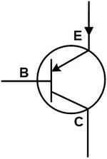
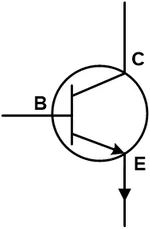
A bipolar junction transistor is a current-controlled semiconductor device with three terminals: base, collector, and emitter. In amplifier operation, a small base-emitter signal controls a larger collector current. The two main BJT polarities are NPN and PNP.
| Item | NPN BJT | PNP BJT |
|---|---|---|
| Usual current direction | Conventional collector current flows from collector to emitter. | Conventional emitter current flows from emitter to collector. |
| Base-emitter bias for conduction | Base is more positive than emitter. | Base is more negative than emitter. |
| Emitter arrow | Arrow points out. | Arrow points in. |
| Use in cascode stages | Common in positive-supply amplifier examples. | Used in complementary or negative-supply versions. |
Applications of BJT Cascode Amplifiers
BJT cascode amplifiers are commonly used where a single common-emitter stage does not provide enough high-frequency performance. Typical applications include RF front ends, IF amplifiers, video amplifiers, high-speed analog stages, current-buffered gain stages, and internal gain stages of analog ICs.
How to Use This Calculator Safely
Use the calculator to estimate a starting point, then check the design against the selected transistor datasheet. Confirm maximum collector-emitter voltage, collector current, power dissipation, transition frequency, capacitances, noise requirements, and package thermal limits. For RF or fast analog circuits, include the PCB layout and measurement setup in your verification plan.
Oscilloscope probes, cables, breadboards, and long test leads can add enough capacitance and inductance to change the measured bandwidth. For high-frequency measurements, use proper probing, short grounds, controlled impedance where needed, and an output buffer if the next stage or instrument load would disturb the amplifier.
Common Mistakes to Avoid
| Mistake | Consequence |
|---|---|
| Using gain formulas without checking headroom | The amplifier may clip because the two stacked transistors do not have enough voltage margin. |
| Ignoring transistor capacitances | The real bandwidth may be much lower than the simple resistor-based estimate. |
| Driving a heavy capacitive load directly | The output may show peaking, slow response, or oscillation. |
| Building high-frequency prototypes on a breadboard | Parasitic capacitance and inductance can dominate the circuit behavior. |
| Forgetting temperature variation | VBE, β, leakage, and bias current can shift with temperature. |
FAQ
Is a cascode amplifier the same as a cascade amplifier?
No. A cascade amplifier simply connects amplifier stages in sequence. A cascode amplifier is a specific topology that combines a common-emitter or common-source stage with a common-base or common-gate stage.
Why does a cascode amplifier need more supply voltage?
The two transistors are stacked vertically in the signal path. Each transistor needs enough voltage across it to stay in the active region, so the circuit usually needs more headroom than a single-transistor common-emitter amplifier.
Can this calculator predict exact RF performance?
No. It gives useful first-order estimates, but exact RF performance depends on transistor models, PCB parasitics, layout, source and load impedance, decoupling, and measurement setup.
When should I add an output buffer?
Add a buffer when the following stage, cable, probe, or load resistance would significantly reduce gain or bandwidth. A buffer can isolate the high-impedance cascode output node from external loading.
Related Online Calculation Tools
BJT Transistor as a Switch, Saturation Calculator - estimates base resistor and saturation conditions for BJT switching circuits.
Wide Band Differential Amplifier Calculator - calculates gain, bias, and frequency-response values for wideband differential amplifier designs.
Op-Amp Voltage and Gain Calculator - calculates output voltage and gain for inverting and non-inverting op-amp circuits.
Ohm's Law Calculator - calculates voltage, current, resistance, and power.