Product
 Brand
Brand Articles
 Tools
Tools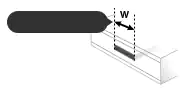

PCB Trace Width Calculator Overview
The PCB Trace Width Calculator estimates the copper trace width required to carry a specified current while keeping the temperature rise within a selected limit. It can also help estimate trace resistance, voltage drop, power loss, and final operating temperature when trace length and ambient temperature are provided.
Trace width is an important part of PCB design because copper conductors heat up when current flows through them. If a trace is too narrow, it can run hot, create excessive voltage drop, damage solder mask or laminate, reduce reliability, or fail under fault conditions.
What Is a PCB Trace Width Calculator?
A PCB trace width calculator uses a current-carrying model to estimate the minimum copper width for a given current, copper thickness, and allowable temperature rise. Many online calculators use the older IPC-2221 curve-fit formulas because they are simple and easy to implement.
The result should be treated as an engineering estimate, not a final guarantee. Real trace temperature depends on copper planes, nearby copper area, board thickness, solder mask, airflow, vias, component heating, ambient temperature, and how long the current is applied. Modern high-reliability designs often compare IPC-2221 estimates with IPC-2152 guidance, simulation, or measurement.
IPC-2221 Trace Width Formula
The IPC-2221-style calculation first estimates the required copper cross-sectional area:
Area(mils²) = [Current / (k × Temperature Rise^b)]^(1 / c)
Then the trace width is calculated from copper thickness:
Width(mils) = Area(mils²) / [Copper Thickness(oz) × 1.378]
| Layer Type | k | b | c |
|---|---|---|---|
| External layer | 0.048 | 0.44 | 0.725 |
| Internal layer | 0.024 | 0.44 | 0.725 |
In this formula, copper thickness is entered as copper weight in ounces per square foot. One ounce copper is approximately 1.378 mil, or about 35 µm, thick.
Input Parameters Explained
| Input | Meaning | Typical Unit |
|---|---|---|
| Current | The RMS or DC current expected to flow through the trace. | A |
| Temperature rise | The allowed increase above ambient temperature when current flows. | °C |
| Copper thickness | The copper weight or finished copper thickness used on the board layer. | oz or µm |
| Layer type | Whether the trace is on an external layer or buried internal layer. | external or internal |
| Ambient temperature | The air or board environment temperature before trace self-heating. | °C |
| Trace length | The length used to estimate resistance, voltage drop, and power loss. | mm, cm, or inch |
Example Calculation
Suppose an external PCB trace must carry 2 A with a 10 °C temperature rise limit on 1 oz copper.
For an external layer, use k = 0.048, b = 0.44, and c = 0.725.
Area = [2 / (0.048 × 10^0.44)]^(1 / 0.725)
Area ≈ 30.8 mils²
Width = 30.8 / (1 × 1.378) ≈ 22.4 mils
This is about 0.57 mm. In a real board, designers often add margin after checking voltage drop, copper tolerance, nearby heat sources, manufacturing rules, and IPC-2152 or measured data.
External vs Internal PCB Traces
| Trace Location | Thermal Behavior | Design Implication |
|---|---|---|
| External layer | Can release heat to surrounding air and adjacent copper more easily. | Usually allows a narrower trace for the same current and temperature rise. |
| Internal layer | Heat must move through dielectric material before reaching the board surface. | Usually needs a wider trace for the same current and temperature rise. |
IPC-2221 and IPC-2152
IPC-2221 provides generic printed board design guidance and is widely used in older trace-width calculators. Its simple formulas are convenient, but they are based on curve fitting and do not model every board condition.
IPC-2152 focuses specifically on current-carrying capacity in printed board design. It considers the relationship between conductor size, current, temperature rise, board construction, nearby copper, vias, planes, and other thermal factors. For production designs, high-current boards, dense layouts, or safety-critical hardware, use IPC-2152 guidance or validated thermal measurement instead of relying only on the simplified IPC-2221 formula.
Trace Resistance, Voltage Drop, and Power Loss
Once trace width is known, the calculator can estimate resistance if trace length and copper thickness are provided. Resistance then gives voltage drop and dissipated power:
Voltage Drop = Current × Resistance
Power Loss = Current² × Resistance
These values matter in low-voltage power rails, motor drivers, LED drivers, battery paths, current-sense layouts, and high-current switching circuits. A trace can meet a temperature-rise target but still create too much voltage drop for the circuit.
Common Copper Thickness Values
| Copper Weight | Approximate Thickness | Typical Use |
|---|---|---|
| 0.5 oz | 17 µm | Fine signal routing and low-current boards. |
| 1 oz | 35 µm | Common default copper thickness for many PCBs. |
| 2 oz | 70 µm | Power boards, motor drivers, LED boards, and higher-current rails. |
| 3 oz and above | 105 µm and above | Heavy copper designs that need special manufacturing review. |
How to Use the Calculator
Enter the expected current, allowed temperature rise, copper thickness, and layer type. If available, also enter ambient temperature and trace length so the calculator can estimate operating temperature, trace resistance, voltage drop, and power loss.
After getting the width, compare it with your PCB manufacturer's minimum and preferred trace widths. Then add design margin for copper thickness tolerance, board stackup, airflow, component heating, solder mask coverage, and current transients.
Practical Design Factors
| Factor | Why It Matters |
|---|---|
| Nearby copper planes | Planes and pours can spread heat and reduce trace temperature. |
| Thermal vias | Vias can move heat between layers and share current when designed correctly. |
| Solder mask | Solder mask can slightly affect heat transfer and available surface cooling. |
| Ambient temperature | A trace that is safe at 25 °C may be too hot in an enclosed product at 60 °C. |
| Current waveform | Pulsed current, RMS current, duty cycle, and peak current must be considered correctly. |
| Manufacturing tolerance | Finished copper thickness and etched width may differ from nominal values. |
Common Mistakes to Avoid
| Mistake | Correct Approach |
|---|---|
| Using external-layer constants for an internal trace. | Select the correct layer type because internal traces usually run hotter. |
| Confusing ambient temperature with temperature rise. | Temperature rise is the increase above ambient, not the final operating temperature. |
| Ignoring voltage drop. | Check resistance and voltage drop, especially on low-voltage high-current rails. |
| Assuming copper weight is exact. | Review finished copper thickness and fabrication tolerance with the PCB supplier. |
| Using the calculator as final proof for safety-critical designs. | Validate with IPC-2152 guidance, simulation, prototypes, or temperature measurement. |
When a Trace Width Calculator Is Not Enough
Use deeper analysis when the board carries high current, operates in a sealed enclosure, has high ambient temperature, uses heavy copper, includes wide copper pours, depends on thermal vias, or must meet safety, automotive, medical, aerospace, or compliance requirements.
In those cases, compare calculator output with IPC-2152 data, PCB manufacturer recommendations, thermal simulation, and measured temperature on a prototype. For fault current or fuse coordination, also evaluate short-circuit behavior and conductor fusing limits.
FAQ
Does a wider trace always run cooler?
Usually yes, but the full temperature depends on board construction, copper area, airflow, nearby heat sources, and how heat leaves the trace.
Is 1 oz copper always 35 µm thick?
It is a common approximation. Finished copper thickness can vary because of base copper, plating, and fabrication process. Confirm finished copper with the PCB manufacturer.
Should I use IPC-2221 or IPC-2152?
IPC-2221 formulas are useful for quick estimates. IPC-2152 is more appropriate when current-carrying capacity and temperature rise need closer design review.
Can I replace a wide trace with several narrower traces?
Sometimes, but current sharing and thermal behavior must be checked. Trace length, via placement, copper distribution, and connection geometry determine how current divides.
Related Online Calculation Tools
Ohm's Law Calculator - calculates voltage, current, resistance, and power.
Wire AWG Size Conversion Calculator - converts AWG, diameter, area, and circular mil values.
Voltage Drop Calculator - estimates voltage drop in conductors.
Parallel and Series Resistor Calculator - calculates equivalent resistance for resistor networks.