High-Frequency Silicon Carbide MOSFETs using Resonant Gate Driver Circuits
| Topics covered in this article: |
| Ⅰ. Proposed Gate Driver Circuit |
| Ⅱ. Experimental Setup and Results |
| Ⅲ. Conclusion |
Although silicon devices have reached their limitations, the growing demand for high power density, performance, compactness, and transient response has increased the need for high switching frequency operations. Due to this, wide bandgap (WBG) materials like silicon carbide (SiC) and gallium nitride (GaN) have gained recognition as viable alternatives to silicon due to their superior properties. SiC MOSFETs combine the low on-state resistance of IGBTs with the low switching losses of Si MOSFETs, making them highly suitable for high-power processing at high switching frequencies. Similarly, GaN devices exhibit exceptional power processing capabilities in high-frequency applications, further contributing to their appeal.

Fig 1: MOSFET gate drive circuit and its gate-charge Characteristic
Researchers have used the resonant gate driver (RGD) circuit to address power consumption challenges. By replacing the conventional gate resistance with an inductance element, the RGD circuit recovers and recycles energy, reducing power consumption and reliance on the power supply. Using VLSI technologies, the RGD circuit can be integrated into a low-power gate driver IC with optocoupler functionality, consuming significantly less power than current ICs. The RGD circuit eliminates ringing and the need for damping resistors, enabling higher switching speeds. By leveraging parasitic inductances created by PCB traces, the RGD circuit converts them into useful resonant inductances. This advancement reduces the size of hold-up capacitors used in power electronic converters, improving performance during power outages.
Ⅰ. Proposed Gate Driver Circuit
Fig. 1 illustrates the proposed resonant gate driver (RGD) circuit designed to operate a SiC MOSFET with gate voltage requirements of -5 V and +20 V during switching. To facilitate analysis and simplify the design, VCC is chosen as +20 V, and VEE as -5 V. Assuming a constant input capacitance (Ciss), the circuit operates in two stages: resonance and clamping, as depicted in Fig. 2 along with the associated waveforms.

Fig 2: Turn-on transition (a) resonance stage. (b) clamping stage. and (c) switching states of BJTs and waveforms of i(Lr) and Vgs.
A. Turn-On Transition
Each switching transition comprises a resonance stage and a clamping stage. In the resonance stage, energy is efficiently recycled, while in the clamping step, any lost energy is replenished from the gate supply. Consequently, power consumption occurs only during the clamping phase.
Initially, the main switch 'Q' is in the off-state (Vgs = -5 V), S4 is in the on-state, and v(Cb) is set to 7.5 V due to the self-balancing feature, which will be explained. Given that Cb is selected to have a higher value than Ciss, the voltage ripple across Cb remains minimal, allowing Cb to function as a voltage source. The voltage across Cb is denoted as Vg.
B. Turn-Off Transition
Two stages are involved during the turn-off transition, which closely resembles the turn-on transition: the resonance stage and the clamping stage. The process begins by turning on S3 at t3 to initiate resonance, and at t4, S4 is turned on while S3 is turned off to achieve clamping. The voltage transition of Vgs during resonance aims to go from 20 V to -5 V, with Vi = 20 V.
However, due to losses from parasitic resistances, BJT, and diode forward voltage drop, Vgs exceeds -5 V, leading to a voltage loss Δvg2. VEE compensates for this loss during the clamping stage. Fig. 2(c) displays the waveforms of Vgs and i(Lr), representing the switching states of BJTs during the turn-off transition. S4 remains in a turn-on state until the turn-on transition of the main switch is triggered.
C. Switching Circuit for the BJTs
The proposed gate driver design involves four BJTs, consisting of two PNP and two NPN BJTs, which must be switched in a specific order. A more streamlined approach is used instead of employing four isolated drive circuits. A pulse from the optocoupler IC, with amplitudes VEE and VCC, is utilized along with a circuit comprising multiple resistors (R) and capacitors (C). These components facilitate the switching of the BJTs and are represented by the red dotted lines in Fig. 2a. It provides the switching pulses for BJTs S2 and S4 while point 2b delivers the switching pulses for BJTs S1 and S3. Assuming that the MOSFET Q is initially in an off-state, with Vgs = -5 V and VOUT = -5 V, the voltage VPG is 0, as indicated in Fig. 2.
D. Self-balancing of the voltage across Cb
The proposed RGD circuit operates based on the principle of series resonance. During the turn-on transition, when the initial voltage (Vgs) across Ciss is VEE, the desired outcome is for Vgs to reach VCC after the resonance is achieved.

Equation 1
The value of voltage source Vg is calculated by Equation 1 to achieve the desired voltage transitions across Ciss from VEE to VCC. Cb in Figure 2 serves as a voltage source Vg. Also, the value of v(Cb) in a steady state is determined by Equation 1. But, the initial value of v(Cb) may deviate from the value given by Equation 1, depending on the switch's initial state. Over successive switching cycles, v(Cb) gradually converges to the value dictated by Equation 1.
Ⅱ. Experimental Setup and Results
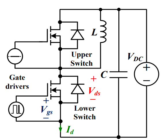
A Double Pulse Test (DPT) fixture has been developed to validate the performance of the proposed RGD circuit. Careful measures were taken to minimize stray inductances, capacitances, and resistances while maintaining a compact PCB size. Initially, both the CGD and proposed RGD circuits were experimentally implemented with a dummy capacitor of equivalent Ciss instead of an actual MOSFET. This allowed for the evaluation of gate driver power consumption and Vgs transition times without the influence of the Miller effect.

Fig 3: Voltage levels of SiC MOSFET during switching transitions.
The SiC MOSFET was switched using the CGD circuit, the proposed RGD circuit, and a previously reported RGD circuit, with waveforms displayed in Fig. 3 The resonant inductor current (iLr) was measured by the voltage difference across a 1 Ω resistance in series with the inductor. The rise and fall times of the MOSFET, obtained from Fig. 3, were found to be 23nS and 20nS, respectively, for the CGD circuit, closely matching the datasheet values.
Ⅲ. Conclusion
An experiment was conducted to validate the proposed universal RGD circuit operating on the series resonance principle. The circuit demonstrated its capability to generate both unipolar and bipolar gate voltages, with equal or unequal magnitudes. By utilizing two series of capacitors connected across one of its supplies and a resonant inductor, the circuit ensured a balanced common point, which acted as a voltage source in the series resonance.
The proposed RGD circuit exhibited a significant reduction in power consumption compared to the traditional CGD. The circuit's design considerations, such as minimizing losses from parasitic and dynamic resistances in the resonant path and selecting appropriate BJTs and diodes, played a significant role in achieving these power savings. The reduced power consumption of the gate driver resulted in energy savings and contributed to a smaller and more cost-effective gate driver power supply. The proposed RGD circuit, with its improved power efficiency, finds its place in high-frequency applications of any voltage-controlled power switch.
 Discovering New and Advanced Methodology for Determining the Dynamic Characterization of Wide Bandgap DevicesSaumitra Jagdale15 March 20242478
For a long era, silicon has stood out as the primary material for fabricating electronic devices due to its affordability, moderate efficiency, and performance capabilities. Despite its widespread use, silicon faces several limitations that render it unsuitable for applications involving high power and elevated temperatures. As technological advancements continue and the industry demands enhanced efficiency from devices, these limitations become increasingly vivid. In the quest for electronic devices that are more potent, efficient, and compact, wide bandgap materials are emerging as a dominant player. Their superiority over silicon in crucial aspects such as efficiency, higher junction temperatures, power density, thinner drift regions, and faster switching speeds positions them as the preferred materials for the future of power electronics.
Read More A Comprehensive Guide to FPGA Development BoardsUTMEL11 September 202514967
This comprehensive guide will take you on a journey through the fascinating world of FPGA development boards. We’ll explore what they are, how they differ from microcontrollers, and most importantly, how to choose the perfect board for your needs. Whether you’re a seasoned engineer or a curious hobbyist, prepare to unlock new possibilities in hardware design and accelerate your projects. We’ll cover everything from budget-friendly options to specialized boards for image processing, delve into popular learning paths, and even provide insights into essential software like Vivado. By the end of this article, you’ll have a clear roadmap to navigate the FPGA landscape and make informed decisions for your next groundbreaking endeavor.
Read More Applications of FPGAs in Artificial Intelligence: A Comprehensive GuideUTMEL29 August 20253654
This comprehensive guide explores FPGAs as powerful AI accelerators that offer distinct advantages over traditional GPUs and CPUs. FPGAs provide reconfigurable hardware that can be customized for specific AI workloads, delivering superior energy efficiency, ultra-low latency, and deterministic performance—particularly valuable for edge AI applications. While GPUs excel at parallel processing for training, FPGAs shine in inference tasks through their adaptability and power optimization. The document covers practical implementation challenges, including development complexity and resource constraints, while highlighting solutions like High-Level Synthesis tools and vendor-specific AI development suites from Intel and AMD/Xilinx. Real-world applications span telecommunications, healthcare, autonomous vehicles, and financial services, demonstrating FPGAs' versatility in mission-critical systems requiring real-time processing and minimal power consumption.
Read More 800G Optical Transceivers: The Guide for AI Data CentersUTMEL24 December 20254003
The complete guide to 800G Optical Transceiver standards (QSFP-DD vs. OSFP). Overcome supply shortages and scale your AI data center with Utmel Electronic.
Read More Xilinx FPGAs: From Getting Started to Advanced Application DevelopmentUTMEL09 September 20254334
This guide is your comprehensive roadmap to understanding and mastering the world of Xilinx FPGA technology. From selecting your first board to deploying advanced AI applications, we'll cover everything you need to know to unlock the potential of these remarkable devices. The global FPGA market is on a significant growth trajectory, expected to expand from USD 8.37 billion in 2025 to USD 17.53 billion by 2035. This surge is fueled by the relentless demand for high-performance, adaptable computing in everything from 5G networks and data centers to autonomous vehicles and the Internet of Things (IoT). This guide will walk you through the key concepts, tools, and products in the Xilinx ecosystem, ensuring you're well-equipped to be a part of this technological revolution.
Read More
Subscribe to Utmel !
![NBSG16BAR2]() NBSG16BAR2
NBSG16BAR2ON Semiconductor
![MOC3021VM]() MOC3021VM
MOC3021VMON Semiconductor
![TDA7803A-ZSX]() TDA7803A-ZSX
TDA7803A-ZSXSTMicroelectronics
![HCS362-I/ST]() HCS362-I/ST
HCS362-I/STMicrochip Technology
![MOC3041SVM]() MOC3041SVM
MOC3041SVMON Semiconductor
![DLPA3000CPFD]() DLPA3000CPFD
DLPA3000CPFDTexas Instruments
![HCS301T/SN]() HCS301T/SN
HCS301T/SNMicrochip Technology
![MOC3021SVM]() MOC3021SVM
MOC3021SVMON Semiconductor
![ATECC508A-MAHCZ-S]() ATECC508A-MAHCZ-S
ATECC508A-MAHCZ-SMicrochip Technology
![MOC3082SM]() MOC3082SM
MOC3082SMON Semiconductor


 Product
 Brand
Brand Articles
 Tools
Tools


