Product
 Brand
Brand Articles
 Tools
Tools
HF PCB Circuit Design 10 Questions
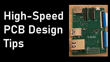
High-Speed PCB Design Tips - Phil's Lab #25
01
How to deal with some theoretical conflicts in actual wiring?
Basically, it's good to separate modules and numbers. Care should be taken not to cross the MOAT and not to let the power supply and signal return current path grow too large.
Crystal oscillator is a simulated positive feedback oscillation circuit. To have a stable oscillation signal, loop gain and phase specifications must be met. However, the oscillating specifications of the analog signals are very susceptible to interference, which may not be completely isolated even with ground guard traces. And too far away, the noise on the ground plane will also affect the positive feedback oscillation circuit. Therefore, be sure to put the crystal oscillator and chip distance into possible close.
It is true that there are many conflicts between high-speed wiring and EMI requirements. However, the basic principle is that due to the resistance capacitance or Ferrite Bead added by EMI, some electrical characteristics of the signal cannot be caused to fail to meet the specifications. Therefore, it is best to use the technique of arranging wiring and PCB stacking to solve or reduce EMI problems, such as high-speed signal lining. Finally, resistor capacitance or Ferrite Bead method was used to reduce the damage to the signal.
02
How to solve the contradiction between manual wiring and automatic wiring of high speed signal?
Nowadays, most of the automatic cabling devices in strong cabling software have set constraints to control the winding mode and the number of holes. EDA companies sometimes vary widely in setting the capabilities and constraints of winding engines. For example, whether there are enough constraints to control how serpentine lines wind, whether there are enough constraints to control the spacing of difference pairs, etc. This will affect whether the automatic wiring out of the wiring can conform to the designer's idea.
In addition, the difficulty of manual wiring adjustment is also absolutely related to the ability of the winding engine. For example, the wire pushing capacity, through the hole pushing capacity, and even the wire on copper coating pushing capacity and so on. So, choose a cabler with strong winding engine ability, it is the way to solve.
03
In high-speed PCB design, copper can be deposited in the blank area of the signal layer, but how should copper deposited in multiple signal layers be distributed on grounding and power supply?
Generally in the blank area copper coating most of the case is grounded. Just pay attention to the distance between copper and the signal line when copper is applied next to the high-speed signal line, because the copper applied will reduce the characteristic impedance of the line. Also be careful not to affect the characteristic impedance of other layers, as in the dual strip line construction.
04
Can the signal line above the power plane be used to calculate the characteristic impedance using the microstrip line model? Can the signal between the power supply and the ground plane be calculated using a ribbon-line model?
Yes, both the power plane and the ground plane must be considered as reference planes when calculating the characteristic impedance. For example, four-layer board: top layer - power layer - stratum - bottom layer. In this case, the model of top layer's wiring characteristic impedance is a microstrip line model with power plane as reference plane.
05
Can software automatically generate test points on high-density PCB that meet the test requirements of mass production in general?
Whether the test points generated automatically by general software can meet the test needs depends on whether the specifications of the added test points meet the requirements of the testing machine. In addition, if the wiring is too dense and the specification for adding test points is strict, it may not be possible to automatically add test points to each segment of the line. Of course, you need to manually complete the test areas.
06
Will the addition of test points affect the quality of high-speed signals?
Whether it affects the signal quality depends on how the test points are added and how fast the signal is. Basically, the added test point does not use the existing perforation (via or DIP pin) as the test point. It may be added to or pulled from the line. The former is equivalent to adding a very small capacitor in line, the latter is an extra branch.
Both of these two conditions have more or less influence on high-speed signals, and the degree of influence is related to the frequency speed and edge rate of signal. The influence can be obtained through simulation. In principle, the smaller the test point, the better (of course, to meet the requirements of the test machine) the shorter the branch, the better.
07
How to connect the ground wire between several PCB systems?
When the signal or power supply between each PCB board is connected to each other, for example, A board has power supply or signal to B board, there must be an equal amount of current from the floor flow back to A board (this is Kirchoffcurrent law). The current in this layer will find its way back to the lowest impedance. Therefore, the number of pins assigned to the formation should not be too low at each interface, either power or signal connection, to reduce impedance and thus reduce formation noise.
It is also possible to analyze the entire current loop, especially the larger part of the current, and adjust the connection of the ground or ground to control the flow of the current (for example, to create a low impedance in one place so that most of the current flows through that place), reducing the impact on other more sensitive signals.
08
What are the principles for properly selecting the point at which the PCB is grounded to the housing?
chassis ground to provide a path of low impedance to return current anThe principle of selecting PCB and shell ground is to use d control the return current. For example, usually in the vicinity of high frequency devices or clock generators, fixed screws can be used to connect the PCB ground to the chassis ground, so as to minimize the entire current loop area and reduce electromagnetic radiation.
09
Which aspects should PCB DEBUG start from?
As far as digital circuits are concerned, three things must first be determined in order:
(1)Make sure that all power supply values meet the design requirements. Some systems with multiple power supplies may require a certain order and speed between the power supplies;
(2)Ensure that all clock signal frequencies are working properly and there are no non-monotonic problems on signal edges;
(3)Verify that the reset signal meets the specification requirements.
If all this is normal, the chip should signal the first cycle. Then DEBUG according to the operating principle of the system and bus protocol.
10
In the case of the fixed size of the circuit board, if the design needs to accommodate more functions, it is often necessary to improve the PCB routing density, but this may lead to increased mutual interference of routing, at the same time, too thin wiring can not reduce the impedance.
So, what are the skills in high-speed (>100MHz) high-density PCB design?
Crosstalkinterference is important in designing high-speed and high-density PCBS because it has a great impact on timing and signal integrity. Here are a few things to look out for:
Control the continuity and matching of wiring characteristic impedance. Distance between cables. The spacing commonly seen is twice the line width. The effect of the spacing on timing and signal integrity can be known through simulation, and the minimum allowable spacing can be found. Signals from different chips may have different results.
Select an appropriate termination mode. Do not allow the two adjacent layers to have the same direction, or even overlap with each other, because crosstalk is larger than that of adjacent layers.
Blind /buried via is used to increase the wiring area. But the cost of PCB board production will increase. It's really hard to do exactly parallel and equal length in practice, but try to do it anyway.
 UTMEL
UTMEL
We are the professional distributor of electronic components, providing a large variety of products to save you a lot of time, effort, and cost with our efficient self-customized service. careful order preparation fast delivery service
1. Can PCB manual and automatic wiring be used together?
PCB manual wiring and automatic wiring can be used together. Both have their own strengths, and the best way is to combine them. Start wiring should be manual wiring as well, is to learn wiring methods, accumulate wiring experience, familiar with the use of software. In having manual wiring experience, familiar with the use of software, you can learn automatic wiring. After both are familiar, can automatic wiring first, modify artificially again complement the inadequacy of automatic wiring, namely fast good.
2. How to add test points to PCB?
The test point is usually a top or bottom pad for contact with the probe of the testing equipment. Therefore, you should place all test pads on the top or bottom layer uniformly, the size of the pad should be appropriate for the probe connection, and the coordinates of the pad should be as integer as possible to facilitate probe positioning. The test pad is generally drawn as a circle and can be connected to the network under test.
3. How does a circuit board in a PCB calculate its test points?
1. The network test point is the point where the data will be finished before the flying needle test and the network will be settled 2 needle bed test point is the test rack of the test rack has up and down how many needles there are points.
4. Must ground wire be connected in PCB design?
It is recommended to connect it, because even if the copper is laid later, the copper skin may be isolated due to the influence of some devices or connections. At that time, there will be two or more places not connected, and there is no flying wire in the PCB, which is easy to cause problems.
 Pull-Down Circuit Guide: Working Principle, Resistor Value, Circuit Design, and ApplicationsUTMEL26 June 202686
Learn how pull-down circuits work, how to choose a pull-down resistor value, and how to design reliable microcontroller inputs, MOSFET gates, reset pins, and sensor interfaces.
Read More HF PCB Circuit Design 10 QuestionsUTMEL16 March 20225341
Hello everyone, I am Rose. Today I want to give you a full explanation about PCB design. I Hope the following ten questions will give you a satisfied answer.
Read More How Many do You Know About the 12 Components Included in the Circuit Board?UTMEL12 February 20228770
We are lucky to live in an era where electronic devices are readily available. These electronic devices, on the other hand, come to us thanks to the incredible components on the circuit board, and we frequently wonder what makes electronic devices operate, how they achieve such massive success, and how they accomplish it. Electronic devices are incredible things; you can't see what's going on within them, but you can see what they're capable of. We'll talk about the wonders of PCBs and how to get past them to construct the circuit board in this article.
Read More![50 Frequently Asked Questions about PCB Layout [Q&A]](https://res.utmel.com/Images/Article/b5ce2a0a-d37c-4243-aff3-df7b2da2db0f.jpg "50 Frequently Asked Questions about PCB Layout [Q&A]") 50 Frequently Asked Questions about PCB Layout [Q&A]UTMEL16 November 20217153
50 Frequently Asked Questions about PCB Layout [Q&A]UTMEL16 November 20217153In the design of electronic products, PCB layout and routing is an important step, and the quality of PCB layout and routing will directly affect the performance of the circuit.
Read More An Overview of Development BoardUTMEL18 December 202515288
The development board is a circuit board used for embedded system development. Development boards are generally customized by embedded system developers according to development needs.
Read More
Subscribe to Utmel !
![PSK-20D-9-DIN]() PSK-20D-9-DIN
PSK-20D-9-DINCUI Inc
![SPMA24301SCC]() SPMA24301SCC
SPMA24301SCCCarlo Gavazzi
![PSK-10D-3-DIN]() PSK-10D-3-DIN
PSK-10D-3-DINCUI Inc
![PSK-20D-15-DIN]() PSK-20D-15-DIN
PSK-20D-15-DINCUI Inc
![ERM04A110B]() ERM04A110B
ERM04A110BArtesyn Embedded Power
![WA101]() WA101
WA101XP Power
![DG06D2405A]() DG06D2405A
DG06D2405ADelta Groups
![DC4-150-1005]() DC4-150-1005
DC4-150-1005Integrated Power Designs
![CSV1600BP-3]() CSV1600BP-3
CSV1600BP-3Artesyn Embedded Power
![MP4-1W-1W-10]() MP4-1W-1W-10
MP4-1W-1W-10Emerson