Product
 Brand
Brand Articles
 Tools
Tools
PCB Design Guidelines
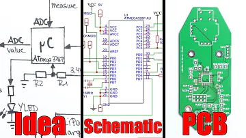
From Idea to Schematic to PCB - How to do it easily!
Ⅰ. Fine-tune your component layout
Component placement is both a science and art in the PCB designing process, requiring strategic consideration of the circuit board's primary components. The way you put your electronic components will affect how easily your circuit board is to create and how well it fulfills your original design criteria, despite the fact that this procedure can be difficult.
Although there is a general order for component placement, such as connections, printed circuit board mounting devices, power circuits, precision circuits, and important circuits being placed in that order, there are several specific rules to remember, including:
Orientation-Make sure that identical components are facing the same way, as this will aid in a quick and error-free welding procedure.
Arrangement-Avoid putting smaller components behind bigger components, as the soldering of large components may damage small components and cause mounting issues.
To simplify assembly processes, it is advised that all surface mount (SMT) components be placed on the same side of the circuit board, and all through-hole (TH) components are placed on the top of the circuit board.
One last PCB design tip to keep in mind: when employing mixed-technology components (through-hole and surface mount components), the manufacturer may demand additional assembly processes, which may raise your overall cost.

Good chip component orientation (left) and bad chip component orientation (right)

Good component placement (left) and bad component placement (right)
Ⅱ. Properly place power, ground, and signal wiring
Place power, ground, and signal traces after the components are in place to guarantee that your signal has a clean and trouble-free path. Please keep the following rules in mind throughout this step of the layout process:
1) Locate the power supply and ground plane layer
The power and ground plane layers should always be placed inside the circuit board while maintaining symmetry and centering. This prevents your circuit board from bending, which is linked to the proper placement of your components.
To ensure a firm and stable trace width and eliminate component-to-component daisy-chain power connections, it is recommended to use a common channel for each power source when powering the IC.
2) Signal wire routing connection
After that, connect the signal wires according to the schematic's design. It is usually advisable to take the shortest and most direct path between components.
If your components must be fixed and positioned in a horizontal path without deviation, it is recommended that the wires be routed primarily horizontally where the circuit board components exit and then vertical wiring be performed after the exit.
The components will be fixed in the horizontal direction due to the migration of the solder during soldering. As may be seen in the upper portion of the diagram below. As the solder flows during soldering, the signal routing mechanism in the lower half of the picture below may cause component deflection.

Recommended wiring method (arrows indicate the direction of solder flow)

Not recommended wiring method (arrows indicate the direction of solder flow)
3) Define the network width
Your design may necessitate many networks carrying differing currents, which will determine the network width required. It is recommended that low-current analog and digital signals have a width of 0.010" (10mil) to meet this basic criterion. It's time to widen your line when the current exceeds 0.3 amps. To make the conversion procedure easier, here is a free line width calculator.
Ⅲ. Effective isolation
Large voltage and current spikes in the power supply circuit can interfere with your low-voltage current control circuit, as you may have discovered. Follow these tips to reduce the risk of interference:
Isolation-Make sure each power supply is isolated from both power and control ground. If you have to connect them in the PCB, make sure it's as close to the end of the power path as feasible.
Placement-If you have a ground plane on the middle layer, make sure to provide a tiny impedance channel to help shield your control signal from power circuit interference. To keep your digital and analog worlds separate, follow the same rules.
Please try to bridge the analog ground exclusively through analog signal lines to reduce capacitive coupling caused by the positioning of a large ground plane and traces above and below it.
Isolation of components as an example (digital and analog)

Ⅳ. Solve the heat problem
Have you ever caused circuit performance to deteriorate or even circuit board damage due to heat issues? Numerous difficulties have plagued many designers since heat dissipation is not taken into account. Here are some pointers to remember while dealing with heat dissipation issues:
1) Identify troublesome components
The first step is to consider which components on the board will dissipate the most heat. This can be accomplished by first locating the component's "thermal resistance" rating on the datasheet, and then transferring the created heat according to the rules. Of course, radiators and cooling fans can be used to keep component temperatures low, and important components should be kept away from any sources of excessive heat.
2) Add a hot air pad
The inclusion of hot air pads to circuit boards makes them more manufacturable. Wave soldering applications on high copper content components and multilayer circuit boards require them. Because maintaining the process temperature is challenging, hot air pads on through-hole components are always recommended to make the soldering process as simple as possible by lowering the heat dissipation rate at the component pins.
Use hot air pads for any through-holes or vias that link to the ground plane or power plane as a general guideline. You can add teardrops to the pad connection line in addition to the hot air pad to offer additional copper foil/metal support. Mechanical and thermal stress will be reduced as a result of this.
Typical hot air pad connection method

Ⅴ. Popularization of hot air pads
Solder emptiness, de-wetting, or cold solder on circuit board components are common problems for Process or SMT engineers in many manufacturers. There is a definite rate of non-wetting failure regardless of how the process conditions are changed or the temperature of the reflow soldering furnace is adjusted for non-wetting flaws. What exactly is it?
Leaving aside the issue of component and circuit board oxidation, it has been discovered that a big part of this type of improper soldering is caused by a lack of circuit board layout design, the most prevalent of which is the soldering of specific components. After reflow soldering, the pins are joined to a large area of copper, resulting in poor soldering of the solder pins of these components. Due to identical conditions, some hand-soldered components may also create false soldering or over soldering issues, and some may even be heated for too long. Soldering destroys the component.
During circuit design, a substantial amount of copper foil is typically put on a PCB to serve as power (Vcc, Vdd, or Vss) and ground (GND, Ground). The pins of some control circuits (ICs) and electronic components are usually directly attached to these large-area copper foils.
Unfortunately, heating these large-area copper foils to the temperature of melting tin takes longer than heating individual solder pads (i.e., the heating is slower) and the heat dissipation is faster. Soldering problems are likely to occur when one end of a large area of copper foil wiring is connected to small components such as small resistors and small capacitors, but the other end is not, due to inconsistent tin melting and solidification time; if the reflow soldering temperature profile is changed. If the solder feet of these components attached to a large piece of copper foil are not adjusted properly and the preheating time is insufficient, virtual soldering will occur because they cannot reach the melting temperature.
The solder feet of these components attached to a wide sheet of copper foil evaporate too quickly during Hand Soldering, therefore they cannot be soldered within the specified time. Package soldering and virtual soldering are the two most common unwanted events. The solder is just applied to the component's solder foot and is not connected to the circuit board's pads. The entire solder joint will appear to be spherical; additionally, the operator constantly raises the temperature of the soldering iron in order to solder the solder foot to the circuit board, or heats it for an excessive amount of time, causing the component to exceed the heat-resistant temperature. Without realizing it, you've been harmed. As indicated in the diagram below.

Package welding, cold welding, or virtual welding
There may be a remedy now that the problem has been identified. To remedy this type of soldering problem produced by the solder feet of the huge copper foil connecting components, we will typically require the usage of a Thermal Relief pad (hot air solder pad). As seen in the diagram below, the wire on the left is not connected with hot air pads, whereas the wiring on the right is. The contact area between the pad and the huge copper foil is only a few thin lines, as can be seen. The temperature loss on the soldering pad can be considerably reduced in this manner, resulting in a better soldering outcome.

Use Thermal Relief pad (hot air solder pad) comparison
Ⅵ. Check your work
When you hum and hum all the elements together for production, it's simple to become overwhelmed and find the problem at the end of the design project. As a result, double- and triple-checking your design work at this point could be the difference between manufacturing success and disaster.
To aid in the quality control process, we always recommend beginning with electrical rule checking (ERC) and design rule checking (DRC) to ensure that your design complies with all rules and limitations. You may simply examine gap widths, line widths, common manufacturing settings, high-speed requirements, and short circuits using these two systems.
When your ERC and DRC produce error-free results, it's a good idea to double-check each signal's wiring, from the schematic to the PCB, and verify one signal line at a time to make sure you didn't miss anything. Additionally, use your design tool's detection and shielding functions to check that your PCB layout materials match your schematic.

 UTMEL
UTMEL
We are the professional distributor of electronic components, providing a large variety of products to save you a lot of time, effort, and cost with our efficient self-customized service. careful order preparation fast delivery service
1. What is the relationship between PCB and IC (integrated circuit)?
Integrated circuit generally refers to the integration of chips, like the Northbridge chip on the motherboard, inside the CPU, they are all called integrated circuits, and the original name is also called integrated block. The PCB refers to the circuit board that we usually see, as well as printing solder chips on the circuit board. The understanding of the relationship between the two: integrated circuit (IC) is soldered on the PCB board; PCB board is the carrier of the integrated circuit (IC).
2. Why do PCBs need to be copper-clad?
Pouring copper has many functions. Pouring copper on the reverse side of the double panel and connecting it to the ground can reduce interference, increase the laying range of the ground wire, reduce low impedance, and so on. Therefore, after the wiring of the pcb board is basically completed, it is often necessary to pour copper.
3. What is the difference between PCBA board and PCB board?
1. The difference in function
The role of PCB is to make a program (including data) that cannot run independently in a multi-program environment, become a basic unit that can run independently, a process that can be executed concurrently with other processes; it is a process that can be executed by the process scheduler in the process. The program code segment executed on the CPU.
Excellent circuit design in PCBA board can save production cost and achieve good circuit performance and heat dissipation performance.

2. Essentially different
PCB is the only sign of the existence of a process, and the PCB process control block is a static description of the process. PCB is the support of electronic components and the provider of circuit connection of electronic components.
The PCBA board is essentially a production process, and the empty PCB board goes through the SMT assembly or the entire manufacturing process of the DIP plug-in.
 HF PCB Circuit Design 10 QuestionsUTMEL16 March 20225327
Hello everyone, I am Rose. Today I want to give you a full explanation about PCB design. I Hope the following ten questions will give you a satisfied answer.
Read More How Many do You Know About the 12 Components Included in the Circuit Board?UTMEL12 February 20228726
We are lucky to live in an era where electronic devices are readily available. These electronic devices, on the other hand, come to us thanks to the incredible components on the circuit board, and we frequently wonder what makes electronic devices operate, how they achieve such massive success, and how they accomplish it. Electronic devices are incredible things; you can't see what's going on within them, but you can see what they're capable of. We'll talk about the wonders of PCBs and how to get past them to construct the circuit board in this article.
Read More![50 Frequently Asked Questions about PCB Layout [Q&A]](https://res.utmel.com/Images/Article/b5ce2a0a-d37c-4243-aff3-df7b2da2db0f.jpg "50 Frequently Asked Questions about PCB Layout [Q&A]") 50 Frequently Asked Questions about PCB Layout [Q&A]UTMEL16 November 20217131
50 Frequently Asked Questions about PCB Layout [Q&A]UTMEL16 November 20217131In the design of electronic products, PCB layout and routing is an important step, and the quality of PCB layout and routing will directly affect the performance of the circuit.
Read More An Overview of Development BoardUTMEL18 December 202515230
The development board is a circuit board used for embedded system development. Development boards are generally customized by embedded system developers according to development needs.
Read More PCB Design GuidelinesUTMEL21 December 20217486
Hello everyone, I am Rose. Today I will provide you a comprehensive guideline of PCB design.
Read More
Subscribe to Utmel !
![AMF24US09]() AMF24US09
AMF24US09XP Power
![JMR0312S12]() JMR0312S12
JMR0312S12XP Power
![AQM200PS48]() AQM200PS48
AQM200PS48XP Power
![LRSA1616-2828-901]() LRSA1616-2828-901
LRSA1616-2828-901Bel Power Solutions
![LRSA6048-1215-900]() LRSA6048-1215-900
LRSA6048-1215-900Bel Power Solutions
![LRSA6024-1228-900]() LRSA6024-1228-900
LRSA6024-1228-900Bel Power Solutions
![LRSA6060-1212-901]() LRSA6060-1212-901
LRSA6060-1212-901Bel Power Solutions
![LRSA3024-2430-900]() LRSA3024-2430-900
LRSA3024-2430-900Bel Power Solutions
![AM1PS-1203SJZ]() AM1PS-1203SJZ
AM1PS-1203SJZaimtec
![AM1LS-2405SJZTR]() AM1LS-2405SJZTR
AM1LS-2405SJZTRaimtec