Introduction to Five Types of Classic Power Supply Circuits
| Topics covered in this article: |
| Ⅰ. Power Supply |
| Ⅱ. Switching power supply |
| Ⅲ. DC-DC power supply |
| Ⅳ. Charging circuit |
| Ⅴ. A constant current source |
Ⅰ. Power Supply
1. 3~25V voltage adjustable voltage regulator circuit
This regulated power supply's adjustable range may be set arbitrarily between 3.5V and 25V, the output current is high, and an adjustable Zener tube circuit is employed to achieve a good and steady output voltage.
Working principle: After rectification and filtering, R1 supplies DC voltage to the regulating tube's base, causing the regulating tube to switch on. When V1 is activated, voltage passes through RP and R2 to activate V2, and then V3 is activated. V1, the emitter and collector voltages of V2 and V3 do not change at this point (its function is identical to that of the Zener tube); changing RP can produce a stable output voltage; and the ratio of R1, RP, R2, and R3 determine the output voltage value of this circuit.
Component selection:
Transformer T selects 80W~100W, input AC220V, output double winding AC28V.
FU1 selects 1A, and FU2 selects 3A~5A.
VD1, VD2 select 6A02.
RP uses a common potentiometer of about 1W, and the resistance value is 250K~330K.
C1 selects 3300µF/35V electrolytic capacitors, C2 and C3 select 0.1µF monolithic capacitors, and C4 selects 470µF/35V electrolytic capacitors.
R1 selects 180~220Ω/0.1W~1W, R2, R4, R5 selects 10KΩ, 1/8W.
V1 selects 2N3055 , V2 selects 3DG180 or 2SC3953, and V3 selects 3CG12 or 3CG80.
3~25V voltage adjustable voltage regulator circuit

Figure. 1 3~25V Voltage Adjustable Voltage Regulator Circuit
2. 10A 3~15V Regulated Adjustable Power Supply Circuit
It is impossible to overhaul computers or electronic production without a regulated power source. The following shows a regulated power supply with a DC voltage that can be adjusted constantly between 3 and 15 volts and a maximum current of 10 amps. The voltage regulation is more exact thanks to the TL431 standard voltage source integrated circuit. It can basically meet the typical maintenance use if there are no specific needs. The circuit can be seen in the diagram below.
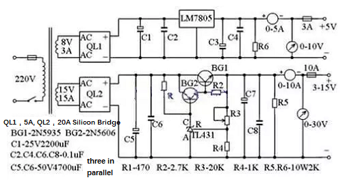
Figure. 2 10A 3~15V Regulated Adjustable Power Supply Circuit
Its working principle is divided into two parts: a fixed 5V1.5A regulated power supply circuit and a high-precision high-current voltage stabilizing circuit that can be adjusted continuously from 3 to 15V.
The first part's circuit is pretty simple. The C1 electrolytic capacitor filters the DC voltage rectified by the secondary 8V AC voltage of the transformer through the silicon bridge QL1, and then the 5V three-terminal voltage regulator block LM7805 can provide a fixed voltage at the output without any adjustment. When overhauling the computer board, this 5V1A regulated power supply can be used as an internal power source.
The second part is similar to a regular series regulated power supply, with the exception that it uses a high-precision standard voltage source integrated circuit TL431 with temperature compensation characteristics, which simplifies the circuit, lowers the cost, and improves voltage regulation performance.
The resistor R4, the voltage regulator tube TL431, and the potentiometer R3 in the diagram produce a constantly adjustable constant voltage source that provides the reference voltage for BG2's base. The stability of the voltage regulator tube TL431 is determined by the voltage regulator value, which is continuously modifiable. If you wish to enhance the adjustable voltage range of the piezoelectric power supply, you can vary the resistance values of R4 and R3, but the secondary voltage of the transformer should also be raised.
The transformer's power can be adjusted according to the output current, and the secondary voltage is around 15 volts. The bridge rectification rectifier tube QL uses a 15-20A silicon bridge has a compact structure and a mounting screw in the center that can be directly placed on the chassis' aluminum plate, which helps with heat dissipation.
A high-current NPN type metal-shell silicon tube is used in the adjustment tube. If the chassis allows, get a large heat sink to increase the heat dissipation area due to the high heat generation. You can utilize a lower power if you don't require a lot of currents. The volume can be reduced by using a silicon tube.
For filtering, three 50V4700uF electrolytic capacitors C5 and C7 are utilized in parallel, resulting in a more stable high current output. Furthermore, this capacitor should be obtained in a large quantity. 50V4700uF is also used to identify those with a lesser capacity. It's best not to utilize it. It is easy to fail when exposed to frequent voltage fluctuations or when not utilized for an extended period of time.
Finally, there's the power transformer to consider. You can replace the transformer with a ready-made switching power supply of more than 200W if you don't have the ability to wind it yourself and can't find one. The voltage regulation performance can be increased further in this manner, while the production cost is kept low. Other electronic components have no specific requirements, and they can function smoothly after installation without a lot of tweaking.
Ⅱ. Switching power supply
1. PWM switching power supply integrated control IC-UC3842 working principle
The internal block diagram and pin diagram of the UC3842 are shown in the diagram below. The UC3842 uses a pulse width controlled modulation mode with a fixed operating frequency. There are a total of 8 pins. The following are the functions of each pin:
1The pin is the error amplifier's output end, and the external resistance-capacitance element is employed to improve the error amplifier's gain and frequency characteristics.
The feedback voltage input terminal is located on the second pin. This pin's voltage is compared to the 2.5V reference voltage of the error amplifier's non-inverting terminal to generate an error voltage, which controls the pulse width.
3The pin is the input endpoint for current detection. When the detecting voltage surpasses 1V, the pulse width is shortened, resulting in intermittent operation of the power supply.
4The timing terminal is the pin, and the external resistance-capacitance time constant, f=1.8/(RTCT), determines the internal oscillator's working frequency. The common ground end is the foot.
6The pin is a push-pull output terminal with a totem pole internal, a rise and fall duration of only 50ns, and a driving capacity of 1A.
7The pin is the power supply end of the DC power supply, and the chip's power consumption is 15mW; it has the function of under-voltage and over-voltage locking.
8The pin is the 50mA load-capable 5V reference voltage output terminal.
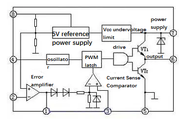
Figure. 3 UC3842 Internal Block Diagram
The UC3842 is a PWM switching power supply integrated controller with great performance, a wide range of applications, and a simple layout. It is mostly used for switching power supply controlled by an audio terminal because it has only one output terminal.
The voltage input terminal on the UC3842 is pin 7, and its beginning voltage range is 16-34V. When the power is turned on and the VCC is 16V, the input voltage Schmitt comparator delivers a high level to the 5V fern regulator, which generates a 5V reference voltage. Voltage. Vcc can vary between 10V and 34V without altering the circuit's operating state until the Schmitt comparator flips to a high level (after the chip starts to work). The Schmitt comparator flips back to low level when Vcc falls below 10V, and the circuit stops working.
The reference voltage detection logic comparator reaches a high level signal to the output circuit when the reference voltage source has a 5V reference voltage output. Simultaneously, the oscillator will emit an f=/Rt.Ct oscillation signal based on the external Rt and Ct parameters of pin 4. This signal will be directly connected to the totem pole circuit's input, while the other will be added to the PWM pulse width to the RS trigger's setting. The output end of the current detecting comparator is connected to the bit end, the R end of the RS-type PWM pulse width modulator. The duty adjustment control terminal is the R terminal. When the R terminal voltage rises, the Q terminal pulse widens, and the pulse width sent from pin 6 also widens (the duty cycle increases); when the R terminal voltage drops, the Q terminal pulse narrows and the pulse width sent from pin 6 also narrows (the duty cycle decreases); when the R terminal voltage drops, the Q terminal pulse narrows and the pulse width sent from pin 6 also narrows (the duty cycle decreases) (the duty cycle decreases).
The figure depicts the timing of each UC3842 point. There is signal output only when point E is high level, and when points a and b are both high level, point d transmits high level and point c sends low level; otherwise, point d sends low level and point c sends high level. ② The output voltage sampling signal, also known as the feedback signal, is usually linked to this pin. When the voltage on pin 2 rises, the voltage on pin 1 drops, and the voltage on the R terminal drops as well, making the pulse on pin 6 smaller; on the other hand, the pulse on pin 6 widens.
The current sensing terminal is the 3 pin; typically, a tiny resistance sampling resistor is connected in series with the power tube's source or emitter; the current flowing through the switch tube is transformed into a voltage, which is then introduced into the environment pin. The 6 pin stops the pulse output when the load is short-circuited or other factors cause the current of the power tube to increase, and the voltage on the sampling resistor exceeds 1V, thereby protecting the power tube from damage.
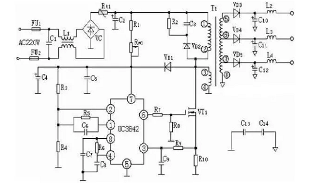
Figure. 4 PWM Switching Power Supply Integrated Control IC-UC3842
2. 12V, 20W switching DC stabilized power supply circuit composed of TOP224P
The 12V, 20W switching DC stabilized power supply circuit composed of TOP224P is shown in the figure.
The circuit includes two integrated circuits: the TOP224P three-terminal single-chip switching power supply (IC1) and the PC817A linear optocoupler (IC2). The AC power is rectified and filtered by UR and Cl to produce DC high voltage Ui, which powers the high-frequency transformer T's primary winding.
VDz1 and VD1 reduce the ringing voltage by clamping the voltage spike caused by leakage inductance to a safe level. VDz1 uses a P6KE200 transient voltage suppressor with a 200V reverse breakdown voltage, whereas VDL uses a UF4005 ultra-fast recovery diode with a 1A/600V reverse breakdown voltage.
V, C2, Ll, and C3 rectify and filter the secondary winding voltage to produce a 12V output voltage Uo. The sum of the VDz2 steady voltage Uz2, the forward voltage drop UF of the LED in the optocoupler, and the voltage drop on R1 determines the Uo value.
Change the turns ratio of the high-frequency transformer and the voltage regulation setting of VDz2 to get different output voltages. To assist load regulation at light loads, R2 and VDz2 offer a phantom load for the 12V output. The bias voltage required by TOP224P is given after the feedback winding voltage is rectified and filtered by VD3 and C4. The control terminal current is adjusted by R2 and VDz2, and the output duty cycle is changed to achieve voltage regulation.
The common-mode chokes coil L2 can minimize the common-mode leakage current generated by the primary winding linked to the D terminal's high voltage switching waveform. C7 is a protection capacitor that is used to filter out interference created by the primary and secondary winding coupling capacitors. The fundamentals and harmonics of the primary winding current generate differential mode leakage current, which is reduced by C6. C5 can determine the self-starting frequency as well as filter out the peak current provided to the control terminal. Together with R1 and R3, it also compensates for the control loop.

Figure. 5 12V, 20W Switching DC Stabilized Power Supply Circuit Composed of TOP224P
The main technical indicators of this power supply are as follows:
AC input voltage range u=85~265V;
Input grid frequency fLl=47~440Hz;
Output voltage (Io=1.67A)Uo=12V;
Maximum output current IOM=1.67A;
Continuous output power Po=20W(TA=25℃, or 15W(TA=50℃);
Voltage regulation η=78%;
Maximum output ripple voltage ±60mV;
Working temperature range TA=0~50℃.
Ⅲ. DC-DC power supply
1. 3V to +5V, +12V circuit
The low power supply voltage is used in most battery-powered portable electronic items, which reduces the number of batteries used and helps to achieve the goal of lowering product size and weight. As a result, 35%V is commonly utilized as the working voltage. A regulated power source is essential to maintain the stability and accuracy of circuit operation.
When a circuit employs a 5V working voltage yet requires a greater working voltage, the designer's job becomes more challenging. This article describes a circuit that solves this problem by combining two boost modules and only two batteries.
The circuit has fewer peripheral components, is tiny and light, and produces a reliable output of +5V and +12V, which fits the needs of portable electronic devices. The maximum output current of a +5V power supply is 60mA, while the maximum output current of a +12V power supply is 5mA.
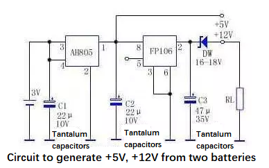
Figure. 6 3V to +5V, +12V Circuit
The circuit is seen in the illustration above. It is made up of two boost modules: AH805 and FP106. When supplied by 3V, the AH805 boost module has a 1.2-3V input and a 5V output, and it can output 100mA current. The FP106 is an SMD booster module with a 46% input voltage, a set output voltage of 291V, and a maximum output current of 40mA. The power-off control terminals AH805 and FP106 are both level-controlled.
Two 1.5V alkaline batteries output 3V voltage to AH805, which outputs +5V voltage, one of which is 5V output, while the other is input to FP106 to generate 28-30V voltage, which is then regulated by a voltage regulator tube to output +12V voltage.
Different output voltages can be achieved by changing the voltage regulator value of the Zener tube, as shown in the figure, and the application is highly flexible. The control power off terminal on the FP106 is the 5pin. The power usage is nearly zero when the electricity is switched off. The power is turned on when the 5pin adds a high level > 2.5V; the power is shut off when the 5pin adds a low-level 0.4v.
2. Use MC34063 to make a 3.6V to 9V circuit
Working status:
With load, output 9.88V, 50.2mA, input 3.65V, 186.7mA, the efficiency is 72 percent (equal to 600mAH battery standby for more than three years).
principle of operation:
The 6 pin of the IC has no power and ceases operating when there is no load. The input terminal's 3.65V operating current is merely 18uA. (equivalent to 600mAH battery standby for more than three years). The EC pole of the 8550 is switched on when there is a load (Q1 has Ieb current), and the IC is powered on. The presence or absence of a load, which is analogous to a battery, determines whether or not the IC operates. The efficiency of using an IC as a voltage converter is great, and the output is stable.
This circuit can be improved by adding more power, which can be used as a "4.2V to 5V mobile power supply without switching". You can use a battery box as a backup power source for your phone.

Figure. 7 Use MC34063 to Make 3.6V to 9V Circuit
Ⅳ. Charging circuit
1. LM358 alkaline battery charger circuit
When it comes to whether or not alkaline batteries can be recharged, there are two schools of thought. Some believe it can be charged, and it has a great effect. Some claim it shouldn't be charged, and the battery instructions suggest there's a risk of an explosion. Alkaline batteries can be recharged, and the number of times they can be recharged is usually between 30 and 50.
In fact, mastering the charging procedure has resulted in two very distinct outcomes. First and foremost, alkaline batteries can undeniably be recharged. At the same time, the battery's description states that alkaline batteries are not rechargeable and that charging them could result in an explosion.
This is likewise correct, although the phrase here is "likely" to result in an explosion. It can also be interpreted as a manufacturer's self-protection disclaimer. Temperature is crucial when charging alkaline batteries. The charging procedure can be completed effectively as long as the battery can be charged without reaching a high temperature. The proper charging technique necessitates a few considerations:
Small current 50MA;
But charge 1.7V, but put 1.3V.
After attempting the charging procedure, some persons categorically state that they are unable to be charged. The charger is usually to blame for issues such as no charging, low power consumption, liquid leaks, and explosions, among others. If the charging current of some fast chargers is greater than 200ma, the battery temperature will be extremely high, it will be hot to the touch, it will leak light, and it will explode in a serious way.
Some individuals charge their batteries with nickel-metal hydride rechargeable battery chargers. Automatic charging halt is not available on low-cost chargers. If the battery is overcharged for an extended period of time, it will leak and explode. Better chargers offer an automated charging stop feature, although the charging stop voltage for NiMH rechargeable batteries is usually set to 1.42V, while the full voltage of alkaline batteries is around 1.7V.
As a result, if the voltage is too low, it appears that the battery cannot be charged, and the power consumption time is short, having little effect. Then there's the battery, which means you shouldn't wait until it's fully dead before recharging it. As a result, no matter how good the battery is, it can be charged three or five times and still have a mediocre effect.
Nanfu alkaline batteries with a voltage of not less than 1.3V are commonly recommended. If you want to charge alkaline batteries, you'll need a charger with a charging current of about 50 milliamps and a charge cut-off voltage of about 1.7 volts. Take a look at your charger at home.
Special alkaline battery chargers, often known as patented devices, are available on the market. In actuality, with a charging voltage of 1.7V and a current of 50ma, it's a simple circuit. I created a basic circuit using the parts LM358 and TL431 that I had on hand. The charging is automatically terminated when the cut-off voltage reaches 1.67V. It only costs two yuan. For the benefit of those who might be interested.
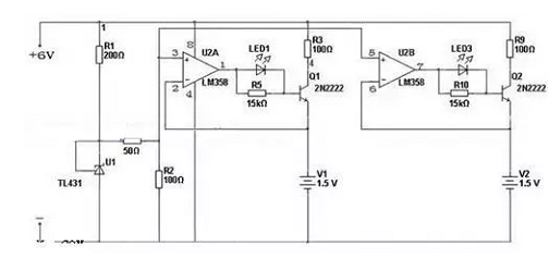
Figure. 8 LM358 Alkaline Battery Charger Circuit
Features:
The open-circuit voltage is 1.5V;
The working temperature range is between -20°C and 60°C, suitable for use in alpine regions;
Continuous discharge capacity at high current is approximately 5 times that of an acid zinc-manganese battery.
It also has excellent low-temperature discharge performance. The number of charging cycles is usually fewer than 30, ranging from 10 to 20. It requires a unique charger, and it is quite simple to lose the ability to charge it.
2. 2.75W medium power USB charger circuit
The LNK613DG from Power Integrations ' LinkSwitch family is used in the design. This design is suited for cell phone or comparable USB charger applications, such as battery chargers for cell phones, USB chargers, or any application requiring constant voltage/constant current characteristics.
The AC input is rectified by diodes D1 to D4, and the DC is filtered by capacitors C1 and C2. To reduce differential mode transmitted EMI noise, L1, C1, and C2 form a -type filter. These, combined with Power Integrations' Transformer E-sheild technology, enable this design to easily meet EN55022 Class B conducted EMI requirements with enough margin without the use of a Y capacitor. The RF1 wire wound resistor is flameproof, fusible, and provides crucial fault protection as well as limiting inrush current during starting.

Figure. 9 2.75W Medium Power USB Charger Circuit
U1 is supplied by an optional bias supply, which reduces the no-load power consumption to less than 40 mW, as shown in the diagram. The quantity of cable drop compensation is determined by the value of bypass capacitor C4. A compensation value of 1F corresponds to a 0.3, 24 AWG USB output cable. (The 10F capacitor adjusts for the USB output cable's 0.49, 26AWG gauge.)
The output voltage is regulated by switching control during the constant voltage stage. By skipping switching cycles, the output voltage is maintained. The ratio of enabling to disable cycles can be adjusted to maintain regulation. This also makes it possible to optimize the converter's efficiency across the whole load range. The current limit is also lowered under light loads (trickle charge) to reduce the transformer flux density, which reduces audible noise and switching losses. The current limit will increase as the load current increases, and fewer cycles will be skipped.
The controller in LinkSwitch-II will switch to the constant current mode when no more switching cycles are skipped (the maximum power point is reached). When the load current needs to be increased, even more, the output voltage will drop. The FB pin voltage is affected by the drop in output voltage.
To prevent the drain voltage spikes induced by leakage inductance, D5, R2, R3, and C3 build an RCD -R clamp circuit. To eliminate oscillation of the drain voltage waveform due to leakage inductance, resistor R3 has a reasonably large value, which prevents excessive oscillation during turn-off and decreases conducted EMI.
The secondary is rectified by diode D7, and it is filtered by diode C7. C6 and R7 work together to minimize both conducted and radiated EMI by limiting transient voltage spikes on D7. When the charger is disconnected from the AC mains, resistor R8 and Zener diode VR1 form an output dummy load, ensuring that the output voltage at no load is within acceptable limits and that the battery does not fully discharge. Feedback resistors R5 and R6 set the maximum operating frequency and the output voltage of the constant voltage stage.
Ⅴ. A constant current source
1. Three-wire constant current source drive circuit
The temperature sensor Pt1000 is driven by the constant current source drive circuit, which converts the resistance signal it detects as temperature changes into a quantifiable voltage signal. The required constant current source in this system should have a constant output current, good temperature stability, large output resistance, output current less than 0.5 mA (Pt1000's upper limit without self-heating effect), one end of the load is grounded, and the output current's polarity can be changed, among other things. Features.
Because temperature has less of an impact on the parameters of the integrated op-amp than it does on the parameters of the transistor or FET, the constant current source made up of integrated op-amps offers superior stability and higher constant current performance. It has been widely employed, particularly in situations where one end of the load must be grounded. As a result, Figure 2 shows a twin op-amp constant current source. UA1 is an adder, UA2 is a follower, and both UA1 and UA2 use the OP07 bipolar operational amplifier, which has low noise, low offset, and high open-loop gain.
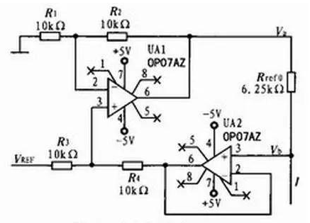
Figure. 10 Three-Wire Constant Current Source Drive Circuit
Assume that the upper and lower ends of the reference resistor Rref in Figure 2 have potentials of Va and Vb and that Va is the non-inverting adder's output. When the resistors R1=R2 and R3=R4 are used, Va=VREFx+Vb is obtained, resulting in a constant current. The source's output current is then:

Figure. 11
The twin op-amp constant current source can be shown to have the following notable characteristics:
The load can be grounded;
The output current is bipolar when the op-amp is fueled by a twin power supply.
It is simple to obtain a stable small current and compensation calibration by changing the input reference VREF or adjusting the size of the reference resistor Rref0, and it is easy to obtain a constant current by changing the input reference VREF or adjusting the size of the reference resistor Rref0.
The voltage across the reference resistor Rref0 will be affected by the terminal voltage Vb of the driving load due to the resistance mismatch. At the same time, because it is a constant current source, Vb will undoubtedly change when the load changes, affecting the constant current source's stability. Obviously, for a high-precision constant current source, this is unacceptable. As a result, the misfit between the four resistors R1, R2, R3, and R4 should be as small as feasible, and the amount and direction of the mismatch between each pair of resistors should be consistent. In practice, a large number of precision resistors in the same batch can be screened, and 4 resistors with close resistance values can be selected.
2. Switching power supply type high withstand voltage constant current source circuit
The creation of the instrument necessitates the use of a continuous current source capable of generating 1MA current over a resistance range of 0 to 3 megohms. One is constructed using a UC3845 and a 12V battery. The transformer employs a color TV high-voltage package, and L1 winds 24 turns on the core of the original high-voltage package with enameled wire, L3 uses a coil from the original high-voltage package, and L2 uses the high-voltage component of the original high-voltage package. To prevent the output voltage from becoming too high, L3 and LM393 form a voltage limiting circuit. The open-circuit output voltage can be adjusted by adjusting R10.
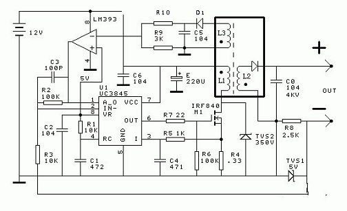
Figure. 12 Switching Power Supply Type High Withstand Voltage Constant Current Source Circuit
1. What is a DC-DC switching power supply?
DC-DC switching power supply is a power supply that uses modern power electronic technology to control the time ratio of switching on and off to maintain a stable output voltage.
2. What are the characteristics of regulated power supply?
[1].Low power consumption and high efficiency. [2]. Small size and light weight. [3]. Wide range of voltage regulation. [4]. The efficiency of filtering is greatly improved, which greatly reduces the capacity and volume of the filtering capacitor. [5]. The circuit forms are flexible and diverse. The disadvantage is that there is more serious switching interference.
3. What are the advantages and disadvantages of switching power supply?
1. High efficiency, ideally no power loss;
2. Small size, the increase of frequency brings miniaturized volume; 3. It can be bucked or boosted output; 4. The input and output are easy to isolate; 5. It is easy to realize multiple output; 6. It can output negative voltage;
7. The input voltage range is very wide.
The disadvantage of switching power supply is that it has output noise and electromagnetic radiation is larger than that of linear power supply.
 LLC Converter with Planar Matrix Transformer for High-Current-High-Power ApplicationsSaumitra Jagdale15 March 20244362
The rise of data centres in recent years, driven by cloud computing and big data, has caused a significant increase in electricity consumption. In the United States alone, it exceeded 70 billion kWh by 2014, making up 1.8% of total national electricity usage.
Read More Enhancing Frequency Stability in Modern Distributed Power SystemsRakesh Kumar, Ph.D.21 September 20243923
The article discusses the importance of primary frequency regulation in maintaining grid stability. It also explores battery energy storage systems, virtual synchronous generators, and advanced control strategies to enhance frequency stability in power systems.
Read More The Impact of SMPS on LED Lighting and Diverse IndustriesUTMEL05 June 20252261
Switched-Mode Power Supplies (SMPS) enhance LED lighting and industries by improving energy efficiency, reliability, and sustainability across diverse applications.
Read More What is Uninterruptible Power Supply (UPS)?UTMEL08 April 20214899
UPS is an uninterruptible power supply containing the energy storage device. It is mainly used to give a part of a device with a higher power stability, providing uninterrupted power supplies.
Read More Switch-mode Power Supply BasicsUTMEL14 December 20207487
Switched-mode Power Supply (SMPS), also known as switching converter, is a high-frequency electric energy conversion device and a type of power supply. Its function is to convert a level of voltage into the voltage or current required by the user through different forms of architecture.
Read More
Subscribe to Utmel !
![DSP1-DC24V-F]() DSP1-DC24V-F
DSP1-DC24V-FPanasonic Electric Works
![JW2SN-DC12V]() JW2SN-DC12V
JW2SN-DC12VPanasonic Electric Works
![ALQ112]() ALQ112
ALQ112Panasonic Electric Works
![JQ1AP-12V-F]() JQ1AP-12V-F
JQ1AP-12V-FPanasonic Electric Works
![ST2-DC24V-F]() ST2-DC24V-F
ST2-DC24V-FPanasonic Electric Works
![LKT1AF-12V]() LKT1AF-12V
LKT1AF-12VPanasonic Electric Works
![DSP1A-DC24V]() DSP1A-DC24V
DSP1A-DC24VPanasonic Electric Works
![ALFG1PF121]() ALFG1PF121
ALFG1PF121Panasonic Electric Works
![ARS14Y4HZ]() ARS14Y4HZ
ARS14Y4HZPanasonic Electric Works
![HE1AN-DC24V]() HE1AN-DC24V
HE1AN-DC24VPanasonic Electric Works


 Product
 Brand
Brand Articles
 Tools
Tools


