
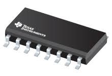
UC3842 PWM controller: Datasheet, Application, Circuit

8 Terminals 12V~28V 8-Pin UC3842 DC to DC converter IC SWITCHING CONTROLLER 1 Outputs Up to 500kHz Transistor Driver
Unit Price: $1.409795
Ext Price: $1.41


8 Terminals 12V~28V 8-Pin UC3842 DC to DC converter IC SWITCHING CONTROLLER 1 Outputs Up to 500kHz Transistor Driver
The UC3842 is a fixed frequency current-mode PWM controller. This article will unlock more details about UC3842. And, there is a huge range of Semiconductors, Capacitors, Resistors and ICs in stock. Welcome RFQ.

UC3842 Switching Power Supply For Battery Charger 3-15V 10A
UC3842 Pinout

UC3842 Pinout
| Pin Number | Pin Name | Description |
| 1 | COMP (Comparator) | It is an output pin that outputs a low impedance 1MHz signal, based on the difference between the set and current-voltage. It is normally connected to the voltage feedback pin of the IC through a resistor and capacitor. |
| 2 | VFB (Voltage Feedback) | It is an input to the error amplifier inside the IC. The difference in voltage level is supplied to this pin |
| 3 | Current Sense | A shunt resistor is used to monitor the current through the circuit, and the voltage across it is provided as feedback to the current sense pin |
| 4 | RT/CT (Timing Resistor/ Timing Capacitor) | The IC has an internal oscillator which can be set using an external resistor and capacitor connected to this pin. |
| 5 | Ground | Connected to the ground of the circuit |
| 6 | Output | This pin outputs the PWM signal based on the feedback provided and we can use this to switch the power electronic device. |
| 7 | Vcc | Supply voltage for the IC (Nominal 11V) |
| 8 | VREF | Reference voltage based on which the PWM signal is produced. |
Pin Description
UC3842 CAD Model
Symbol

UC3842 Symbol
Footprint

UC3842 Footprint
3D Model

UC3842 3D Model
UC3842 Description
The UC3842 is a current-mode PWM controller with a set frequency. This IC was created with minimal external components in mind for Off-Line and DC to DC converter applications, which also provides current-limit control, and a totem-pole output stage designed to source or sink high peak current. The output stage, suitable for driving N-Channel MOSFETs, is low in the off state.
Specifications
- TypeParameter
- Lifecycle Status
Lifecycle Status refers to the current stage of an electronic component in its product life cycle, indicating whether it is active, obsolete, or transitioning between these states. An active status means the component is in production and available for purchase. An obsolete status indicates that the component is no longer being manufactured or supported, and manufacturers typically provide a limited time frame for support. Understanding the lifecycle status is crucial for design engineers to ensure continuity and reliability in their projects.
ACTIVE (Last Updated: 6 days ago) - Factory Lead Time6 Weeks
- Mounting Type
The "Mounting Type" in electronic components refers to the method used to attach or connect a component to a circuit board or other substrate, such as through-hole, surface-mount, or panel mount.
Through Hole - Package / Case
refers to the protective housing that encases an electronic component, providing mechanical support, electrical connections, and thermal management.
8-DIP (0.300, 7.62mm) - Surface Mount
having leads that are designed to be soldered on the side of a circuit board that the body of the component is mounted on.
NO - Number of Pins8
- Weight528.605208mg
- Operating Temperature
The operating temperature is the range of ambient temperature within which a power supply, or any other electrical equipment, operate in. This ranges from a minimum operating temperature, to a peak or maximum operating temperature, outside which, the power supply may fail.
0°C~70°C TA - Packaging
Semiconductor package is a carrier / shell used to contain and cover one or more semiconductor components or integrated circuits. The material of the shell can be metal, plastic, glass or ceramic.
Tube - JESD-609 Code
The "JESD-609 Code" in electronic components refers to a standardized marking code that indicates the lead-free solder composition and finish of electronic components for compliance with environmental regulations.
e4 - Pbfree Code
The "Pbfree Code" parameter in electronic components refers to the code or marking used to indicate that the component is lead-free. Lead (Pb) is a toxic substance that has been widely used in electronic components for many years, but due to environmental concerns, there has been a shift towards lead-free alternatives. The Pbfree Code helps manufacturers and users easily identify components that do not contain lead, ensuring compliance with regulations and promoting environmentally friendly practices. It is important to pay attention to the Pbfree Code when selecting electronic components to ensure they meet the necessary requirements for lead-free applications.
yes - Part Status
Parts can have many statuses as they progress through the configuration, analysis, review, and approval stages.
Active - Moisture Sensitivity Level (MSL)
Moisture Sensitivity Level (MSL) is a standardized rating that indicates the susceptibility of electronic components, particularly semiconductors, to moisture-induced damage during storage and the soldering process, defining the allowable exposure time to ambient conditions before they require special handling or baking to prevent failures
1 (Unlimited) - Number of Terminations8
- ECCN Code
An ECCN (Export Control Classification Number) is an alphanumeric code used by the U.S. Bureau of Industry and Security to identify and categorize electronic components and other dual-use items that may require an export license based on their technical characteristics and potential for military use.
EAR99 - Terminal Finish
Terminal Finish refers to the surface treatment applied to the terminals or leads of electronic components to enhance their performance and longevity. It can improve solderability, corrosion resistance, and overall reliability of the connection in electronic assemblies. Common finishes include nickel, gold, and tin, each possessing distinct properties suitable for various applications. The choice of terminal finish can significantly impact the durability and effectiveness of electronic devices.
Nickel/Palladium/Gold (Ni/Pd/Au) - Terminal Position
In electronic components, the term "Terminal Position" refers to the physical location of the connection points on the component where external electrical connections can be made. These connection points, known as terminals, are typically used to attach wires, leads, or other components to the main body of the electronic component. The terminal position is important for ensuring proper connectivity and functionality of the component within a circuit. It is often specified in technical datasheets or component specifications to help designers and engineers understand how to properly integrate the component into their circuit designs.
DUAL - Terminal Pitch
The center distance from one pole to the next.
2.54mm - Frequency
In electronic components, the parameter "Frequency" refers to the rate at which a signal oscillates or cycles within a given period of time. It is typically measured in Hertz (Hz) and represents how many times a signal completes a full cycle in one second. Frequency is a crucial aspect in electronic components as it determines the behavior and performance of various devices such as oscillators, filters, and communication systems. Understanding the frequency characteristics of components is essential for designing and analyzing electronic circuits to ensure proper functionality and compatibility with other components in a system.
450kHz - Base Part Number
The "Base Part Number" (BPN) in electronic components serves a similar purpose to the "Base Product Number." It refers to the primary identifier for a component that captures the essential characteristics shared by a group of similar components. The BPN provides a fundamental way to reference a family or series of components without specifying all the variations and specific details.
UC3842 - Function
The parameter "Function" in electronic components refers to the specific role or purpose that the component serves within an electronic circuit. It defines how the component interacts with other elements, influences the flow of electrical signals, and contributes to the overall behavior of the system. Functions can include amplification, signal processing, switching, filtering, and energy storage, among others. Understanding the function of each component is essential for designing effective and efficient electronic systems.
Step-Up, Step-Down, Step-Up/Step-Down - Number of Outputs1
- Output Voltage
Output voltage is a crucial parameter in electronic components that refers to the voltage level produced by the component as a result of its operation. It represents the electrical potential difference between the output terminal of the component and a reference point, typically ground. The output voltage is a key factor in determining the performance and functionality of the component, as it dictates the level of voltage that will be delivered to the connected circuit or load. It is often specified in datasheets and technical specifications to ensure compatibility and proper functioning within a given system.
13.5V - Output Type
The "Output Type" parameter in electronic components refers to the type of signal or data that is produced by the component as an output. This parameter specifies the nature of the output signal, such as analog or digital, and can also include details about the voltage levels, current levels, frequency, and other characteristics of the output signal. Understanding the output type of a component is crucial for ensuring compatibility with other components in a circuit or system, as well as for determining how the output signal can be utilized or processed further. In summary, the output type parameter provides essential information about the nature of the signal that is generated by the electronic component as its output.
Transistor Driver - Input Voltage-Nom
Input Voltage-Nom refers to the nominal or rated input voltage that an electronic component or device is designed to operate within. This parameter specifies the voltage level at which the component is expected to function optimally and safely. It is important to ensure that the actual input voltage supplied to the component does not exceed this nominal value to prevent damage or malfunction. Manufacturers provide this specification to guide users in selecting the appropriate power supply or input voltage source for the component. It is a critical parameter to consider when designing or using electronic circuits to ensure reliable performance and longevity of the component.
15V - Analog IC - Other Type
Analog IC - Other Type is a parameter used to categorize electronic components that are integrated circuits (ICs) designed for analog signal processing but do not fall into more specific subcategories such as amplifiers, comparators, or voltage regulators. These ICs may include specialized analog functions such as analog-to-digital converters (ADCs), digital-to-analog converters (DACs), voltage references, or signal conditioning circuits. They are typically used in various applications where precise analog signal processing is required, such as in audio equipment, instrumentation, communication systems, and industrial control systems. Manufacturers provide detailed specifications for these components to help engineers select the most suitable IC for their specific design requirements.
SWITCHING CONTROLLER - Output Configuration
Output Configuration in electronic components refers to the arrangement or setup of the output pins or terminals of a device. It defines how the output signals are structured and how they interact with external circuits or devices. The output configuration can determine the functionality and compatibility of the component in a circuit design. Common types of output configurations include single-ended, differential, open-drain, and push-pull configurations, each serving different purposes and applications in electronic systems. Understanding the output configuration of a component is crucial for proper integration and operation within a circuit.
Positive - Output Current
The rated output current is the maximum load current that a power supply can provide at a specified ambient temperature. A power supply can never provide more current that it's rated output current unless there is a fault, such as short circuit at the load.
1A - Voltage - Supply (Vcc/Vdd)
Voltage - Supply (Vcc/Vdd) is a key parameter in electronic components that specifies the voltage level required for the proper operation of the device. It represents the power supply voltage that needs to be provided to the component for it to function correctly. This parameter is crucial as supplying the component with the correct voltage ensures that it operates within its specified limits and performance characteristics. It is typically expressed in volts (V) and is an essential consideration when designing and using electronic circuits to prevent damage and ensure reliable operation.
12V~28V - Control Features
Control features in electronic components refer to specific functionalities or characteristics that allow users to manage and regulate the operation of the component. These features are designed to provide users with control over various aspects of the component's performance, such as adjusting settings, monitoring parameters, or enabling specific modes of operation. Control features can include options for input/output configurations, power management, communication protocols, and other settings that help users customize and optimize the component's behavior according to their requirements. Overall, control features play a crucial role in enhancing the flexibility, usability, and performance of electronic components in various applications.
Frequency Control - Topology
In the context of electronic components, "topology" refers to the arrangement or configuration of the components within a circuit or system. It defines how the components are connected to each other and how signals flow between them. The choice of topology can significantly impact the performance, efficiency, and functionality of the electronic system. Common topologies include series, parallel, star, mesh, and hybrid configurations, each with its own advantages and limitations. Designers carefully select the appropriate topology based on the specific requirements of the circuit to achieve the desired performance and functionality.
Boost, Buck, Buck-Boost, Flyback, Forward - Control Mode
In electronic components, "Control Mode" refers to the method or mode of operation used to regulate or control the behavior of the component. This parameter determines how the component responds to input signals or commands to achieve the desired output. The control mode can vary depending on the specific component and its intended function, such as voltage regulation, current limiting, or frequency modulation. Understanding the control mode of an electronic component is crucial for proper integration and operation within a circuit or system.
CURRENT-MODE - Frequency - Switching
"Frequency - Switching" in electronic components refers to the rate at which a device, such as a transistor or switching regulator, turns on and off during operation. This parameter is crucial in determining the efficiency and performance of power converters, oscillators, and other circuits that rely on rapid switching. Higher switching frequencies typically allow for smaller component sizes but may require more advanced design considerations to manage heat and electromagnetic interference.
Up to 500kHz - Control Technique
In electronic components, "Control Technique" refers to the method or approach used to regulate and manage the operation of the component. This parameter is crucial in determining how the component functions within a circuit or system. Different control techniques can include analog control, digital control, pulse-width modulation (PWM), and various feedback mechanisms. The choice of control technique can impact the performance, efficiency, and overall functionality of the electronic component. It is important to select the appropriate control technique based on the specific requirements and characteristics of the application in which the component will be used.
PULSE WIDTH MODULATION - Rise Time
In electronics, when describing a voltage or current step function, rise time is the time taken by a signal to change from a specified low value to a specified high value.
50ns - Supply Current-Max (Isup)
Supply Current-Max (Isup) refers to the maximum amount of current that an electronic component can draw from its power supply during operation. It represents the peak current demand of the device under normal operating conditions and is critical for ensuring that the power supply can adequately support the component's needs without risking damage or malfunction. This parameter is essential for designing circuits and selecting appropriate power supply units to prevent overloading and ensure reliable performance.
25mA - Synchronous Rectifier
Synchronous rectification is a technique for improving the efficiency of rectification by replacing diodes with actively controlled switches, usually power MOSFETs or power bipolar junction transistors (BJT).
No - Fall Time (Typ)
Fall Time (Typ) is a parameter used to describe the time it takes for a signal to transition from a high level to a low level in an electronic component, such as a transistor or an integrated circuit. It is typically measured in nanoseconds or microseconds and is an important characteristic that affects the performance of the component in digital circuits. A shorter fall time indicates faster switching speeds and can result in improved overall circuit performance, such as reduced power consumption and increased data transmission rates. Designers often consider the fall time specification when selecting components for their circuits to ensure proper functionality and efficiency.
50 ns - Nominal Input Voltage
The actual voltage at which a circuit operates can vary from the nominal voltage within a range that permits satisfactory operation of equipment. The word “nominal” means “named”.
30V - Max Duty Cycle
Max Duty Cycle refers to the maximum percentage of time that an electronic component, such as a switch or a power supply, can be in an "on" state during a defined time period. It is an important parameter in pulse-width modulated (PWM) systems and helps determine how often a device can operate without overheating or sustaining damage. By specifying the maximum duty cycle, manufacturers provide guidance on the safe operational limits of the component, ensuring reliability and efficiency in various applications.
100 % - Duty Cycle (Max)
The "Duty Cycle (Max)" parameter in electronic components refers to the maximum percentage of time that a signal is active or on within a specific period. It is commonly used in components such as pulse-width modulation (PWM) controllers, oscillators, and timers. A duty cycle of 100% means the signal is always on, while a duty cycle of 0% means the signal is always off. Understanding the maximum duty cycle is important for ensuring proper operation and performance of the electronic component within its specified limits. It is typically expressed as a percentage and helps determine the amount of power or energy being delivered by the signal.
97% - Height5.08mm
- Length9.81mm
- Width6.35mm
- Thickness
Thickness in electronic components refers to the measurement of how thick a particular material or layer is within the component structure. It can pertain to various aspects, such as the thickness of a substrate, a dielectric layer, or conductive traces. This parameter is crucial as it impacts the electrical, mechanical, and thermal properties of the component, influencing its performance and reliability in electronic circuits.
3.9mm - REACH SVHC
The parameter "REACH SVHC" in electronic components refers to the compliance with the Registration, Evaluation, Authorization, and Restriction of Chemicals (REACH) regulation regarding Substances of Very High Concern (SVHC). SVHCs are substances that may have serious effects on human health or the environment, and their use is regulated under REACH to ensure their safe handling and minimize their impact.Manufacturers of electronic components need to declare if their products contain any SVHCs above a certain threshold concentration and provide information on the safe use of these substances. This information allows customers to make informed decisions about the potential risks associated with using the components and take appropriate measures to mitigate any hazards.Ensuring compliance with REACH SVHC requirements is essential for electronics manufacturers to meet regulatory standards, protect human health and the environment, and maintain transparency in their supply chain. It also demonstrates a commitment to sustainability and responsible manufacturing practices in the electronics industry.
No SVHC - RoHS Status
RoHS means “Restriction of Certain Hazardous Substances” in the “Hazardous Substances Directive” in electrical and electronic equipment.
ROHS3 Compliant - Lead Free
Lead Free is a term used to describe electronic components that do not contain lead as part of their composition. Lead is a toxic material that can have harmful effects on human health and the environment, so the electronics industry has been moving towards lead-free components to reduce these risks. Lead-free components are typically made using alternative materials such as silver, copper, and tin. Manufacturers must comply with regulations such as the Restriction of Hazardous Substances (RoHS) directive to ensure that their products are lead-free and environmentally friendly.
Lead Free
Parts with Similar Specs
- ImagePart NumberManufacturerPackage / CaseNumber of PinsNumber of OutputsOutput CurrentFrequency - SwitchingOutput VoltageFactory Lead TimeMoisture Sensitivity Level (MSL)View Compare
![UC3842N]()
UC3842N
8-DIP (0.300, 7.62mm)
8
1
1 A
Up to 500kHz
13.5 V
6 Weeks
1 (Unlimited)
![UC3844AN]()
8-DIP (0.300, 7.62mm)
8
1
200 mA
100kHz
30 V
6 Weeks
1 (Unlimited)
![TL3845P]()
8-DIP (0.300, 7.62mm)
8
1
1 A
Up to 500kHz
5 V
6 Weeks
1 (Unlimited)
![UC3842AN]()
8-DIP (0.300, 7.62mm)
8
1
1 A
Up to 500kHz
15 V
6 Weeks
1 (Unlimited)

UC3842 Feature
Current-Mode PWM controller
Operating Voltage: 12V to 28V
Output pin current: 200 mA
Switching Frequency: 500 kHz
Duty Cycle - Max: 100 %
Operating Supply Current:25 mA
Optimized for Off-line and DC-to-DC Converters
High-Current Totem-Pole Output
UC3842 Application
SMPS (Switch Mode Power Supplies) circuits
DC-DC converter circuits
Electronics power supply
Battery drain circuit
Load machines
UC3842 Equivalent
Equivalent for UC3842: UC3843.
UC3842 Block Diagram

UC3842 Block Diagram
Where to use UC3842
The UC3842 IC is a current Mode PWM Controller, which means it can change the output voltage to the load to provide a constant current. A trimmed oscillator, a temperature corrected reference, a high gain error amplifier, a current detecting comparator, and a high current totem pole output for driving a Power MOSFET are all included in this IC.
In applications such as SMPS, RPS, DC-DC Converters, Line voltage regulators, and so on, the UC3842 can be used to regulate or limit current. So, if you're looking for an IC that can generate PWM signals to control a power switch based on the current flowing through the circuit, this IC would be a good fit.
How to use UC3842
The use of the UC3842 in a circuit is fairly straightforward because it only requires a few components. The following is a sample application circuit taken from the UC3842 datasheet.

How to UC3842 Circuit
The VCC pin's input voltage should be between 12 and 28 volts. The IC's output pin is connected to the gate driver circuit of the to-be-switched Power switch. The VFB (Voltage feedback) pin serves as feedback for controlling the PWM signal. The feedback pin receives the difference voltage across the shunt resistor, which is used to monitor the change in current in the circuit. Through the timing resistor, VREF is utilized to deliver the charging current to the oscillator timing capacitor. VREF must be bypassed to GROUND with a ceramic capacitor attached as close to the pin as possible for reference stability.
UC3842 Package

UC3842 Package
UC3842 Manufacturer
Texas Instruments (TI) emerges as a globally recognized semiconductor manufacturer expanded into 35 countries. It has seen rapid growth. In 1958, TIer firstly introduced the working integrated circuit. And today more than 30,000 TIers worldwide are committed to designing, manufacturing, and selling analogue and embedded processing chips. They aspire to solve challenges as well as change the world through their technologies.
Datasheet PDF
- Datasheets :
- PCN Assembly/Origin :
- PCN Design/Specification :
Popularity by Region
What is UC3842?
The UC3842 is an integrated pulse width modulator (PWM) designed with both these objectives in mind. This IC provides designers an inexpensive controller with which they can obtain all the performance advantages of current-mode operation.
What is switching frequency range of 3842?
The UC3842 and UC3843 oscillators run AT the switching frequency. Each oscillator of the UC3842/3/4/5 family can be used to a maximum of 500 kHz. The UC3842 and UC3843 have a maximum duty cycle of approximately 100%, whereas the UC3844 and UC3845 are clamped to 50% maximum by an internal toggle flip flop.
What is current mode PWM controller?
Glossary Term: Current Mode PWM
Definition. A DC-DC switching regulator regulates its output voltage by varying the peak inductor current on a cycle-by-cycle basis to output a regulated voltage despite variations in load-current and input voltage.
 A Comprehensive Guide to LTC6804HG-2#3ZZPBF Battery Management PMIC
06 March 2024131
![The Guide to BD243 NPN Power Transistor [FAQ]](https://res.utmel.com/Images/Article/d2eaffd3-c961-4ded-aab0-cdd243058476.jpg) The Guide to BD243 NPN Power Transistor [FAQ]
The Guide to BD243 NPN Power Transistor [FAQ]29 March 20223820
 TL494IN Controller: Pinout, Specification, Datasheet
12 May 20218114
 TPS5430 Step-Down Converter: Pinout, Equivalent and Datasheet
26 October 202111017
 STM32F429IIT6 STMicroelectronics: Specification, Datasheet, Manufacturer And Features
11 April 2022861
 NE555 Precision Timer: Features, Specifications and Applications
11 May 20211397
 tsop38238 IR Receiver Sensor
26 March 20225807
 MCP41010 Potentiometer: Circuit, Pinout, and Datasheet
15 October 20217146
 Millimeter Wave Radar: Advantages, Types, and Applications
18 October 202119148
 Towards an Optoelectronic Chip That Mimics the Human Brain
20 April 2022811
 ITA-3: A Step Towards a Sustainable Future for Global ICT and Economy
14 September 20232654
 Understanding SiC MOSFET Power Modules and Ensuring its Short-Circuit Safety
15 March 20242382
 How do We Select Automotive Relays?
30 September 20208482
 Top 5 SR44 Battery Brands for Reliable Power
20 August 20251960
 Power Management Integrated Circuit (PMIC) Guide
10 February 202213227
 The Difference between Switching Power Supply and Ordinary Power Supply
12 July 20221611
Texas Instruments
In Stock: 18
Minimum: 1 Multiples: 1
Qty
Unit Price
Ext Price
1
$1.409795
$1.41
10
$1.329995
$13.30
100
$1.254712
$125.47
500
$1.183691
$591.85
1000
$1.116689
$1,116.69
Not the price you want? Send RFQ Now and we'll contact you ASAP.
Inquire for More Quantity
![LM3485MM/NOPB]() LM3485MM/NOPB
LM3485MM/NOPBTexas Instruments
![LM3478MM/NOPB]() LM3478MM/NOPB
LM3478MM/NOPBTexas Instruments
![LM5085MY/NOPB]() LM5085MY/NOPB
LM5085MY/NOPBTexas Instruments
![UC2825DW]() UC2825DW
UC2825DWTexas Instruments
![UCC28950PWR]() UCC28950PWR
UCC28950PWRTexas Instruments
![LM3488MM/NOPB]() LM3488MM/NOPB
LM3488MM/NOPBTexas Instruments
![UC3845AD8]() UC3845AD8
UC3845AD8Texas Instruments
![LM3150MHX/NOPB]() LM3150MHX/NOPB
LM3150MHX/NOPBTexas Instruments
![UCC28C43DR]() UCC28C43DR
UCC28C43DRTexas Instruments
![UCC25600DR]() UCC25600DR
UCC25600DRTexas Instruments


