
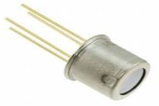
 Product
 Brand
Brand Articles
 Tools
Tools
LM7171 Voltage Feedback Amplifier: Datasheet, Pinout, Schematic

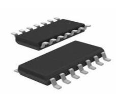
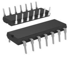
118mA per Channel 2.7μA 70 dB Instrumentational OP Amps 18V 5.5V~36V ±2.75V~18V LM7171 8 Pins 8-SOIC (0.154, 3.90mm Width)


118mA per Channel 2.7μA 70 dB Instrumentational OP Amps 18V 5.5V~36V ±2.75V~18V LM7171 8 Pins 8-SOIC (0.154, 3.90mm Width)
This post covers the datasheet, pinout, schematic and more details about LM7171, a high-speed voltage feedback amplifier.

Electronics: Strange output with a LM7171 opamp (non-inverser amplifier) (3 Solutions!!)
LM7171 Pinout

LM7171 Pinout
| Pin Number | Pin Name | Description |
| 1 | NC | No Connection |
| 2 | -IN | Inverting Power Supply |
| 3 | +IN | Non-inverting Power Suppl: |
| 4 | V. | Supply Voltage |
| 5 | NIC | No Connection |
| 6 | OUTPUT | Output |
| 7 | V+ | Supply Voltage |
| 8 | NC | No Connection |
Pin Description
LM7171 Description
The LM7171 is a high-speed voltage feedback amplifier that has the slewing characteristic of a current feedback amplifier, yet it can be used in all traditional voltage feedback amplifier configurations.
The LM7171 is stable for gains as low as +2 or −1. It provides a very high slew rate at 4100V/µs and a wide unity-gain bandwidth of 200 MHz while consuming only 6.5 mA of supply current.
LM7171 CAD Model
Symbol

LM7171 Symbol
Footprint

LM7171 Footprint
3D Model

LM7171 3D Model
Specifications
- TypeParameter
- Mount
In electronic components, the term "Mount" typically refers to the method or process of physically attaching or fixing a component onto a circuit board or other electronic device. This can involve soldering, adhesive bonding, or other techniques to secure the component in place. The mounting process is crucial for ensuring proper electrical connections and mechanical stability within the electronic system. Different components may have specific mounting requirements based on their size, shape, and function, and manufacturers provide guidelines for proper mounting procedures to ensure optimal performance and reliability of the electronic device.
Surface Mount - Mounting Type
The "Mounting Type" in electronic components refers to the method used to attach or connect a component to a circuit board or other substrate, such as through-hole, surface-mount, or panel mount.
Surface Mount - Package / Case
refers to the protective housing that encases an electronic component, providing mechanical support, electrical connections, and thermal management.
8-SOIC (0.154, 3.90mm Width) - Number of Pins8
- Number of Elements1
- Operating Temperature
The operating temperature is the range of ambient temperature within which a power supply, or any other electrical equipment, operate in. This ranges from a minimum operating temperature, to a peak or maximum operating temperature, outside which, the power supply may fail.
-40°C~85°C - Packaging
Semiconductor package is a carrier / shell used to contain and cover one or more semiconductor components or integrated circuits. The material of the shell can be metal, plastic, glass or ceramic.
Tape & Reel (TR) - Series
In electronic components, the "Series" refers to a group of products that share similar characteristics, designs, or functionalities, often produced by the same manufacturer. These components within a series typically have common specifications but may vary in terms of voltage, power, or packaging to meet different application needs. The series name helps identify and differentiate between various product lines within a manufacturer's catalog.
VIP™ III - JESD-609 Code
The "JESD-609 Code" in electronic components refers to a standardized marking code that indicates the lead-free solder composition and finish of electronic components for compliance with environmental regulations.
e0 - Pbfree Code
The "Pbfree Code" parameter in electronic components refers to the code or marking used to indicate that the component is lead-free. Lead (Pb) is a toxic substance that has been widely used in electronic components for many years, but due to environmental concerns, there has been a shift towards lead-free alternatives. The Pbfree Code helps manufacturers and users easily identify components that do not contain lead, ensuring compliance with regulations and promoting environmentally friendly practices. It is important to pay attention to the Pbfree Code when selecting electronic components to ensure they meet the necessary requirements for lead-free applications.
no - Part Status
Parts can have many statuses as they progress through the configuration, analysis, review, and approval stages.
Obsolete - Moisture Sensitivity Level (MSL)
Moisture Sensitivity Level (MSL) is a standardized rating that indicates the susceptibility of electronic components, particularly semiconductors, to moisture-induced damage during storage and the soldering process, defining the allowable exposure time to ambient conditions before they require special handling or baking to prevent failures
1 (Unlimited) - Number of Terminations8
- ECCN Code
An ECCN (Export Control Classification Number) is an alphanumeric code used by the U.S. Bureau of Industry and Security to identify and categorize electronic components and other dual-use items that may require an export license based on their technical characteristics and potential for military use.
EAR99 - Terminal Finish
Terminal Finish refers to the surface treatment applied to the terminals or leads of electronic components to enhance their performance and longevity. It can improve solderability, corrosion resistance, and overall reliability of the connection in electronic assemblies. Common finishes include nickel, gold, and tin, each possessing distinct properties suitable for various applications. The choice of terminal finish can significantly impact the durability and effectiveness of electronic devices.
Tin/Lead (Sn/Pb) - Packing Method
The packing method in electronic components refers to the technique used to package and protect the component during shipping and handling. It encompasses various forms including tape and reel, tray, tube, or bulk packaging, each suited for different types of components and manufacturing processes. The choice of packing method can affect the ease of handling, storage, and the efficiency of assembly in automated processes. Additionally, it plays a crucial role in ensuring the reliability and integrity of the components until they are used in electronic devices.
TAPE AND REEL - Terminal Position
In electronic components, the term "Terminal Position" refers to the physical location of the connection points on the component where external electrical connections can be made. These connection points, known as terminals, are typically used to attach wires, leads, or other components to the main body of the electronic component. The terminal position is important for ensuring proper connectivity and functionality of the component within a circuit. It is often specified in technical datasheets or component specifications to help designers and engineers understand how to properly integrate the component into their circuit designs.
DUAL - Terminal Form
Occurring at or forming the end of a series, succession, or the like; closing; concluding.
GULL WING - Peak Reflow Temperature (Cel)
Peak Reflow Temperature (Cel) is a parameter that specifies the maximum temperature at which an electronic component can be exposed during the reflow soldering process. Reflow soldering is a common method used to attach electronic components to a circuit board. The Peak Reflow Temperature is crucial because it ensures that the component is not damaged or degraded during the soldering process. Exceeding the specified Peak Reflow Temperature can lead to issues such as component failure, reduced performance, or even permanent damage to the component. It is important for manufacturers and assemblers to adhere to the recommended Peak Reflow Temperature to ensure the reliability and functionality of the electronic components.
235 - Number of Functions1
- Supply Voltage
Supply voltage refers to the electrical potential difference provided to an electronic component or circuit. It is crucial for the proper operation of devices, as it powers their functions and determines performance characteristics. The supply voltage must be within specified limits to ensure reliability and prevent damage to components. Different electronic devices have specific supply voltage requirements, which can vary widely depending on their design and intended application.
5V - Base Part Number
The "Base Part Number" (BPN) in electronic components serves a similar purpose to the "Base Product Number." It refers to the primary identifier for a component that captures the essential characteristics shared by a group of similar components. The BPN provides a fundamental way to reference a family or series of components without specifying all the variations and specific details.
LM7171 - Pin Count
a count of all of the component leads (or pins)
8 - Operating Supply Voltage
The voltage level by which an electrical system is designated and to which certain operating characteristics of the system are related.
18V - Operating Supply Current
Operating Supply Current, also known as supply current or quiescent current, is a crucial parameter in electronic components that indicates the amount of current required for the device to operate under normal conditions. It represents the current drawn by the component from the power supply while it is functioning. This parameter is important for determining the power consumption of the component and is typically specified in datasheets to help designers calculate the overall power requirements of their circuits. Understanding the operating supply current is essential for ensuring proper functionality and efficiency of electronic systems.
6.5mA - Nominal Supply Current
Nominal current is the same as the rated current. It is the current drawn by the motor while delivering rated mechanical output at its shaft.
6.5mA - Output Current
The rated output current is the maximum load current that a power supply can provide at a specified ambient temperature. A power supply can never provide more current that it's rated output current unless there is a fault, such as short circuit at the load.
100mA - Slew Rate
the maximum rate of output voltage change per unit time.
4100V/μs - Amplifier Type
Amplifier Type refers to the classification or categorization of amplifiers based on their design, functionality, and characteristics. Amplifiers are electronic devices that increase the amplitude of a signal, such as voltage or current. The type of amplifier determines its specific application, performance capabilities, and operating characteristics. Common types of amplifiers include operational amplifiers (op-amps), power amplifiers, audio amplifiers, and radio frequency (RF) amplifiers. Understanding the amplifier type is crucial for selecting the right component for a particular circuit or system design.
Voltage Feedback - Common Mode Rejection Ratio
Common Mode Rejection Ratio (CMRR) is a measure of the ability of a differential amplifier to reject input signals that are common to both input terminals. It is defined as the ratio of the differential gain to the common mode gain. A high CMRR indicates that the amplifier can effectively eliminate noise and interference that affects both inputs simultaneously, enhancing the fidelity of the amplified signal. CMRR is typically expressed in decibels (dB), with higher values representing better performance in rejecting common mode signals.
70 dB - Current - Input Bias
The parameter "Current - Input Bias" in electronic components refers to the amount of current required at the input terminal of a device to maintain proper operation. It is a crucial specification as it determines the minimum input current needed for the component to function correctly. Input bias current can affect the performance and accuracy of the device, especially in precision applications where small signal levels are involved. It is typically specified in datasheets for operational amplifiers, transistors, and other semiconductor devices to provide users with important information for circuit design and analysis.
2.7μA - Voltage - Supply, Single/Dual (±)
The parameter "Voltage - Supply, Single/Dual (±)" in electronic components refers to the power supply voltage required for the proper operation of the component. This parameter indicates whether the component requires a single power supply voltage (e.g., 5V) or a dual power supply voltage (e.g., ±15V). For components that require a single power supply voltage, only one voltage level is needed for operation. On the other hand, components that require a dual power supply voltage need both positive and negative voltage levels to function correctly.Understanding the voltage supply requirements of electronic components is crucial for designing and integrating them into circuits to ensure proper functionality and prevent damage due to incorrect voltage levels.
5.5V~36V ±2.75V~18V - Output Current per Channel
Output Current per Channel is a specification commonly found in electronic components such as amplifiers, audio interfaces, and power supplies. It refers to the maximum amount of electrical current that can be delivered by each individual output channel of the component. This parameter is important because it determines the capacity of the component to drive connected devices or loads. A higher output current per channel means the component can deliver more power to connected devices, while a lower output current may limit the performance or functionality of the component in certain applications. It is crucial to consider the output current per channel when selecting electronic components to ensure they can meet the power requirements of the intended system or setup.
118mA - Input Offset Voltage (Vos)
Input Offset Voltage (Vos) is a key parameter in electronic components, particularly in operational amplifiers. It refers to the voltage difference that must be applied between the two input terminals of the amplifier to nullify the output voltage when the input terminals are shorted together. In simpler terms, it represents the voltage required to bring the output of the amplifier to zero when there is no input signal present. Vos is an important parameter as it can introduce errors in the output signal of the amplifier, especially in precision applications where accuracy is crucial. Minimizing Vos is essential to ensure the amplifier operates with high precision and accuracy.
200μV - Gain Bandwidth Product
The gain–bandwidth product (designated as GBWP, GBW, GBP, or GB) for an amplifier is the product of the amplifier's bandwidth and the gain at which the bandwidth is measured.
200MHz - Neg Supply Voltage-Nom (Vsup)
The parameter "Neg Supply Voltage-Nom (Vsup)" in electronic components refers to the nominal negative supply voltage that the component requires to operate within its specified performance characteristics. This parameter indicates the minimum voltage level that must be provided to the component's negative supply pin for proper functionality. It is important to ensure that the negative supply voltage provided to the component does not exceed the maximum specified value to prevent damage or malfunction. Understanding and adhering to the specified negative supply voltage requirements is crucial for the reliable operation of the electronic component in a circuit.
-5V - Unity Gain BW-Nom
Unity Gain Bandwidth, often abbreviated as Unity Gain BW or UGBW, refers to the frequency at which an amplifier can provide a gain of one (0 dB). It is a critical parameter in assessing the performance of operational amplifiers and other amplifying devices, indicating the range of frequencies over which the amplifier can operate without distortion. Unity Gain BW is particularly important in applications where signal fidelity is crucial, as it helps determine the maximum frequency of operation for a given gain level. As the gain is reduced, the bandwidth typically increases, ensuring that the amplifier can still operate effectively across various signal frequencies.
125000 kHz - Voltage Gain
Voltage gain is a measure of how much an electronic component or circuit amplifies an input voltage signal to produce an output voltage signal. It is typically expressed as a ratio or in decibels (dB). A higher voltage gain indicates a greater amplification of the input signal. Voltage gain is an important parameter in amplifiers, where it determines the level of amplification provided by the circuit. It is calculated by dividing the output voltage by the input voltage and is a key factor in determining the overall performance and functionality of electronic devices.
78dB - Power Supply Rejection Ratio (PSRR)
Power Supply Rejection Ratio (PSRR) is a measure of how well an electronic component, such as an operational amplifier or voltage regulator, can reject changes in its supply voltage. It indicates the ability of the component to maintain a stable output voltage despite fluctuations in the input supply voltage. A higher PSRR value signifies better performance in rejecting noise and variations from the power supply, leading to improved signal integrity and more reliable operation in electronic circuits. PSRR is typically expressed in decibels (dB).
75dB - Low-Offset
Low-offset is a parameter used to describe the level of offset voltage in electronic components, particularly in operational amplifiers. Offset voltage refers to the small voltage difference that exists between the input terminals of the amplifier when the input voltage is zero. A low-offset value indicates that this voltage difference is minimal, which is desirable for accurate signal processing and amplification. Components with low-offset specifications are preferred in applications where precision and accuracy are critical, such as in instrumentation and measurement systems. Minimizing offset voltage helps reduce errors and ensures the faithful reproduction of input signals by the amplifier.
NO - Frequency Compensation
Frequency compensation is implemented by modifying the gain and phase characteristics of the amplifier's open loop output or of its feedback network, or both, in such a way as to avoid the conditions leading to oscillation. This is usually done by the internal or external use of resistance-capacitance networks.
YES AVCL>=2 - Low-Bias
Low-bias in electronic components refers to a design or configuration that minimizes the amount of bias current flowing through the component. Bias current is a small, steady current that is used to establish the operating point of a component, such as a transistor or amplifier. By reducing the bias current to a low level, the component can operate with lower power consumption and potentially lower distortion. Low-bias components are often used in applications where power efficiency and signal fidelity are important, such as in audio amplifiers or battery-powered devices. Overall, the low-bias parameter indicates the ability of the component to operate efficiently and accurately with minimal bias current.
NO - Micropower
the use of very small electric generators and prime movers or devices to convert heat or motion to electricity, for use close to the generator.
NO - -3db Bandwidth
The "-3dB bandwidth" of an electronic component refers to the frequency range over which the component's output signal power is reduced by 3 decibels (dB) compared to its maximum output power. This parameter is commonly used to describe the frequency response of components such as amplifiers, filters, and other signal processing devices. The -3dB point is significant because it represents the half-power point, where the output signal power is reduced to half of its maximum value. Understanding the -3dB bandwidth is important for designing and analyzing electronic circuits to ensure that signals are accurately processed within the desired frequency range.
220MHz - Programmable Power
A programmable power supply provides remote control capability of the output voltage(s) via an analog control signal controlled by keypad or rotary switch from the front panel of the power supply or via a computer interface such as RS232, GPIB, or USB.
NO - Wideband
Wideband refers to a characteristic of electronic components or systems that can operate over a broad frequency range. It indicates the ability of the component to handle a wide spectrum of frequencies without significant loss of performance. In applications such as amplifiers, antennas, and filters, wideband components are essential for transmitting and receiving signals across various frequencies, making them versatile for different communication standards and technologies.
YES - Length4.9mm
- Radiation Hardening
Radiation hardening is the process of making electronic components and circuits resistant to damage or malfunction caused by high levels of ionizing radiation, especially for environments in outer space (especially beyond the low Earth orbit), around nuclear reactors and particle accelerators, or during nuclear accidents or nuclear warfare.
No - RoHS Status
RoHS means “Restriction of Certain Hazardous Substances” in the “Hazardous Substances Directive” in electrical and electronic equipment.
Non-RoHS Compliant - Lead Free
Lead Free is a term used to describe electronic components that do not contain lead as part of their composition. Lead is a toxic material that can have harmful effects on human health and the environment, so the electronics industry has been moving towards lead-free components to reduce these risks. Lead-free components are typically made using alternative materials such as silver, copper, and tin. Manufacturers must comply with regulations such as the Restriction of Hazardous Substances (RoHS) directive to ensure that their products are lead-free and environmentally friendly.
Contains Lead
Parts with Similar Specs
LM7171 Features
Easy-to-use voltage feedback topology
Very high slew rate: 4100 V/µs
Wide unity-gain bandwidth: 200 MHz
−3 dB frequency @ AV = +2: 220 MHz
Low supply current: 6.5 mA
High open-loop gain: 85 dB
High output current: 100 mA
Differential gain and phase: 0.01%, 0.02˚
Specified for ±15V and ±5V operation
LM7171 Simplified Schematic Diagram

LM7171 Simplified Schematic Diagram
LM7171 Applications
HDSL and ADSL drivers
Multimedia broadcast systems
Professional video cameras
Video amplifiers
Copiers/scanners/fax
HDTV amplifiers
Pulse amplifiers and peak detectors
CATV/fibre optics signal processing
LM7171 Application Circuits
The LM7171 is a very high speed, voltage feedback amplifier. It consumes only 6.5 mA supply current while providing a unity-gain bandwidth of 200 MHz and a slew rate of 4100V/μs. It also has other great features such as low differential gain and phase and high output current.
The LM7171 is a true voltage feedback amplifier. Unlike current feedback amplifiers (CFAs) with a low inverting input impedance and a high non-inverting input impedance, both inputs of voltage feedback amplifiers (VFAs) have high impedance nodes. The low impedance inverting input in CFAs and a feedback capacitor creates an additional pole that will lead to instability. As a result, CFAs cannot be used in traditional op-amp circuits such as photodiode amplifiers, I-to-V converters and integrators where a feedback capacitor is required.
The class AB input stage in LM7171 is fully symmetrical and has a similar slewing characteristic to the current feedback amplifiers. In the LM7171 Simplified Schematic, Q1 through Q4 form the equivalent of the current feedback input buffer, RE the equivalent of the feedback resistor, and stage A buffers the inverting input. The triple-buffered output stage isolates the gain stage from the load to provide low output impedance.
The application circuits for LM7171 are shown below.

LM7171 Fast Instrumentation Amplifier

LM7171 Multivibrator

LM7171 Pulse Width Modulator

LM7171 Video Line Driver
LM7171 Alternatives
| Parts | Description | Manufacturer |
| LF347N AMPLIFIER CIRCUITS | IC QUAD OP-AMP, 13000 uV OFFSET-MAX, 4 MHz BAND WIDTH, PDIP14, PLASTIC, DIP-14, Operational Amplifier | National Semiconductor Corporation |
| LM101AH/883 AMPLIFIER CIRCUITS | IC OP-AMP, Operational Amplifier | Linear Technology |
| LMC6064IMX AMPLIFIER CIRCUITS | QUAD OP-AMP, 1300uV OFFSET-MAX, 0.1MHz BAND WIDTH, PDSO14, SOP-14 | Rochester Electronics LLC |
| 5962R9950402VDX AMPLIFIER CIRCUITS | Operational Amplifier, 4 Func, 4000uV Offset-Max, BIPolar, CDSO14, CERAMIC, DFP-14 | Defense Logistics Agency |
| 5962-8771002GA AMPLIFIER CIRCUITS | IC DUAL OP-AMP, 500 UV OFFSET-MAX, 1 MHz BANDWIDTH, MBCY8, METAL CAN, TO-99, 8 PIN, Operational Amplifier | National Semiconductor Corporation |
| LPV358MMX/NOPB AMPLIFIER CIRCUITS | IC DUAL OP-AMP, 10000 uV OFFSET-MAX, 0.152 MHz BAND WIDTH, PDSO8, MSOP-8, Operational Amplifier | National Semiconductor Corporation |
| LM358H AMPLIFIER CIRCUITS | DUAL OP-AMP, 9000uV OFFSET-MAX, 1MHz BAND WIDTH, MBCY8, METAL CAN, TO-5, 8 PIN | Texas Instruments |
| LF411ACN/NOPB AMPLIFIER CIRCUITS | IC OP-AMP, 500 UV OFFSET-MAX, 4 MHz BANDWIDTH, PDIP8, DIP-8, Operational Amplifier | National Semiconductor Corporation |
| M38510/10103BCA AMPLIFIER CIRCUITS | IC OP-AMP, 3000 uV OFFSET-MAX, CDIP14, CERAMIC, DIP-14, Operational Amplifier | Defense Supply Center Columbus |
| LF412MH AMPLIFIER CIRCUITS | IC DUAL OP-AMP, 3000 UV OFFSET-MAX, 4 MHz BANDWIDTH, MBCY8, METAL CAN-8, Operational Amplifier | National Semiconductor Corporation |
LM7171 Alternatives
LM7171 Package

LM7171 Package
LM7171 Manufacturer
Texas Instruments (TI) is a global semiconductor firm originating in 1958 and nowadays it has over 30,000 employees who design, conduct and sell analogue and product-differentiating embedded processing components in 35 countries. Aimed at changing the world of tech, TI has put great effort into becoming the solution provider coupled with a vision.
Datasheet PDF
- Datasheets :
Popularity by Region
Is lm7171 an op-amp or a comparator?
The LM7171 is a high-speed voltage feedback amplifier.
What is the LM7171?
The LM7171 is a high-speed voltage feedback amplifier that has the slewing characteristic of a current feedback amplifier, yet it can be used in all traditional voltage feedback amplifier configurations. The LM7171 is stable for gains as low as +2 or −1. It provides a very high slew rate at 4100V/µs and a wide unity-gain bandwidth of 200 MHz while consuming only 6.5 mA of supply current.
Is LM7171 ideal for video and high speed signal processing application?
Yes, It is ideal for video and high-speed signal processing applications such as HDSL and pulse amplifiers. With 100 mA output current, the LM7171 can be used for video distribution, as a transformer driver or as a laser diode driver.
What does LM7171 operate?
It operates on ±15V power supplies allows for large signal swings and provides greater dynamic range and signal-to-noise ratio. The LM7171 offers low SFDR and THD, ideal for ADC/DAC systems. In addition, the LM7171 is specified for ±5V operation for portable applications.
 TJA1043 High-speed Can Transceiver: Datasheet, Application Hints, Test Circuit
01 December 20217363
 XC6220b331PR-G- LDO Voltage Regulator
03 March 20221858
 J111 JFET Transistor: J111 Datasheet, Pinout, Equivalent
12 April 20228518
 IR2110 Driver IC: Equivalent, Pinout and Test Circuit
10 September 202121497
 AVR® ATtiny 4KB 8-bit MCU: Datasheet, Pinout, and Performance Deep Dive
12 February 2026332
 Introduction to MSP430G2x11 and MSP430G2x01 Mixed-Signal Microcontrollers
29 February 2024144
 MLX90614 Infra Red Thermometer: Pinout, Datasheet and Applications
30 July 20217719
 IRF5210 Power MOSFET: Datasheet, Price, Pinout
18 March 20225019
 Spiral wrap choices that keep hoses damage free
15 July 20251125
 What is Field Programmable Gate Array(FPGA)?
27 April 20221284
 The History of Thermometers
15 June 202618722
 Organic Semiconductor Market Set to Reach USD 843.62 Billion by 2032, Driven by Rising Demand for Flexible Electronics
05 October 20232521
 Analysis of Magnetic and Thermal Semiconductor Power Modules
13 March 20242078
 European Chipmakers Experience Decline Following SMIC's Profit Slump
20 November 20233289
 Classification and Working Principle of Ballast Resistor
18 November 20207716
 Huang Renxun: Nvidia Is No Longer a GPU Company
06 April 20222672
Texas Instruments
In Stock
United States
China
Canada
Japan
Russia
Germany
United Kingdom
Singapore
Italy
Hong Kong(China)
Taiwan(China)
France
Korea
Mexico
Netherlands
Malaysia
Austria
Spain
Switzerland
Poland
Thailand
Vietnam
India
United Arab Emirates
Afghanistan
Åland Islands
Albania
Algeria
American Samoa
Andorra
Angola
Anguilla
Antigua & Barbuda
Argentina
Armenia
Aruba
Australia
Azerbaijan
Bahamas
Bahrain
Bangladesh
Barbados
Belarus
Belgium
Belize
Benin
Bermuda
Bhutan
Bolivia
Bonaire, Sint Eustatius and Saba
Bosnia & Herzegovina
Botswana
Brazil
British Indian Ocean Territory
British Virgin Islands
Brunei
Bulgaria
Burkina Faso
Burundi
Cabo Verde
Cambodia
Cameroon
Cayman Islands
Central African Republic
Chad
Chile
Christmas Island
Cocos (Keeling) Islands
Colombia
Comoros
Congo
Congo (DRC)
Cook Islands
Costa Rica
Côte d’Ivoire
Croatia
Cuba
Curaçao
Cyprus
Czechia
Denmark
Djibouti
Dominica
Dominican Republic
Ecuador
Egypt
El Salvador
Equatorial Guinea
Eritrea
Estonia
Eswatini
Ethiopia
Falkland Islands
Faroe Islands
Fiji
Finland
French Guiana
French Polynesia
Gabon
Gambia
Georgia
Ghana
Gibraltar
Greece
Greenland
Grenada
Guadeloupe
Guam
Guatemala
Guernsey
Guinea
Guinea-Bissau
Guyana
Haiti
Honduras
Hungary
Iceland
Indonesia
Iran
Iraq
Ireland
Isle of Man
Israel
Jamaica
Jersey
Jordan
Kazakhstan
Kenya
Kiribati
Kosovo
Kuwait
Kyrgyzstan
Laos
Latvia
Lebanon
Lesotho
Liberia
Libya
Liechtenstein
Lithuania
Luxembourg
Macao(China)
Madagascar
Malawi
Maldives
Mali
Malta
Marshall Islands
Martinique
Mauritania
Mauritius
Mayotte
Micronesia
Moldova
Monaco
Mongolia
Montenegro
Montserrat
Morocco
Mozambique
Myanmar
Namibia
Nauru
Nepal
New Caledonia
New Zealand
Nicaragua
Niger
Nigeria
Niue
Norfolk Island
North Korea
North Macedonia
Northern Mariana Islands
Norway
Oman
Pakistan
Palau
Palestinian Authority
Panama
Papua New Guinea
Paraguay
Peru
Philippines
Pitcairn Islands
Portugal
Puerto Rico
Qatar
Réunion
Romania
Rwanda
Samoa
San Marino
São Tomé & Príncipe
Saudi Arabia
Senegal
Serbia
Seychelles
Sierra Leone
Sint Maarten
Slovakia
Slovenia
Solomon Islands
Somalia
South Africa
South Sudan
Sri Lanka
St Helena, Ascension, Tristan da Cunha
St. Barthélemy
St. Kitts & Nevis
St. Lucia
St. Martin
St. Pierre & Miquelon
St. Vincent & Grenadines
Sudan
Suriname
Svalbard & Jan Mayen
Sweden
Syria
Tajikistan
Tanzania
Timor-Leste
Togo
Tokelau
Tonga
Trinidad & Tobago
Tunisia
Turkey
Turkmenistan
Turks & Caicos Islands
Tuvalu
U.S. Outlying Islands
U.S. Virgin Islands
Uganda
Ukraine
Uruguay
Uzbekistan
Vanuatu
Vatican City
Venezuela
Wallis & Futuna
Yemen
Zambia
Zimbabwe
![LMV722MX]() LMV722MX
LMV722MXTexas Instruments
![LMC6082AIN]() LMC6082AIN
LMC6082AINTexas Instruments
![RC4558P]() RC4558P
RC4558PTexas Instruments
![LMC6482IMM/NOPB]() LMC6482IMM/NOPB
LMC6482IMM/NOPBTexas Instruments
![LM324MX/NOPB]() LM324MX/NOPB
LM324MX/NOPBTexas Instruments
![LM324AM/NOPB]() LM324AM/NOPB
LM324AM/NOPBTexas Instruments
![LMV324IDR]() LMV324IDR
LMV324IDRTexas Instruments
![LMC7101BIM5/NOPB]() LMC7101BIM5/NOPB
LMC7101BIM5/NOPBTexas Instruments
![TLV2372IDR]() TLV2372IDR
TLV2372IDRTexas Instruments
![NE5532P]() NE5532P
NE5532PTexas Instruments


