
 Product
 Brand
Brand Articles
 Tools
Tools
BSS138 MOSFET Guide: Logic-Level N-Channel Transistor Specs & Applications

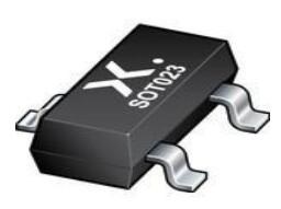
N-Channel Tape & Reel (TR) 3.5Ohm @ 220mA, 10V ±20V 27pF @ 25V 2.4nC @ 10V 50V TO-236-3, SC-59, SOT-23-3


N-Channel Tape & Reel (TR) 3.5Ohm @ 220mA, 10V ±20V 27pF @ 25V 2.4nC @ 10V 50V TO-236-3, SC-59, SOT-23-3
This comprehensive guide provides an in-depth review of the BSS138 MOSFET, exploring its technical specifications, key features, and common applications. We will delve into its performance characteristics, compare it with popular alternatives, and offer practical guidance to help you integrate this powerful component into your next design. Whether you are a seasoned engineer or just starting your journey in electronics, this guide will equip you with the knowledge to make informed decisions and unlock the full potential of the BSS138.
Understanding the BSS138
The onsemi BSS138 is a small-signal N-Channel enhancement-mode MOSFET that has carved out a significant niche in the semiconductor market [1]. Manufactured using onsemi’s proprietary, high-density DMOS technology, this transistor is engineered for efficiency and reliability. Its primary market positioning is as a logic-level MOSFET, meaning it can be controlled directly by the low-voltage signals from microcontrollers (like 3.3V or 5V) without the need for intermediary driver circuits. This feature makes it exceptionally valuable in modern digital electronics, where seamless integration with low-power processors is paramount.
In a market saturated with countless transistors, the BSS138 distinguishes itself through its versatility and accessibility. It is a staple component for a wide array of low-voltage, low-current applications, making it a favorite for both rapid prototyping and mass production. Its presence in the industry-standard SOT-23 package further enhances its appeal, allowing for high-density placement on printed circuit boards (PCBs) and making it suitable for space-constrained designs. The BSS138 is not just a component; it’s a problem-solver for engineers tackling challenges in power management, signal switching, and interfacing between different logic families.
Datasheet PDF
- PCN Design/Specification :
- Datasheets :
BSS138-ON-Semiconductor-datasheet-85430893.pdf
BSS138-Fairchild-Semiconductor-datasheet-47995523.pdf
BSS138-ON-Semiconductor-datasheet-137236190.pdf
BSS138-Fairchild-datasheet-7603324.pdf
BSS138-Fairchild-Semiconductor-datasheet-48066972.pdf
BSS138-ON-Semiconductor-datasheet-71727.pdf
- PCN Assembly/Origin :
- Environmental Information :
- PCN Packaging :
- ReachStatement :
- TechnicalDrawing :
Specifications
- TypeParameter
- Lifecycle Status
Lifecycle Status refers to the current stage of an electronic component in its product life cycle, indicating whether it is active, obsolete, or transitioning between these states. An active status means the component is in production and available for purchase. An obsolete status indicates that the component is no longer being manufactured or supported, and manufacturers typically provide a limited time frame for support. Understanding the lifecycle status is crucial for design engineers to ensure continuity and reliability in their projects.
ACTIVE (Last Updated: 6 days ago) - Factory Lead Time8 Weeks
- Contact Plating
Contact plating (finish) provides corrosion protection for base metals and optimizes the mechanical and electrical properties of the contact interfaces.
Tin - Mount
In electronic components, the term "Mount" typically refers to the method or process of physically attaching or fixing a component onto a circuit board or other electronic device. This can involve soldering, adhesive bonding, or other techniques to secure the component in place. The mounting process is crucial for ensuring proper electrical connections and mechanical stability within the electronic system. Different components may have specific mounting requirements based on their size, shape, and function, and manufacturers provide guidelines for proper mounting procedures to ensure optimal performance and reliability of the electronic device.
Surface Mount - Mounting Type
The "Mounting Type" in electronic components refers to the method used to attach or connect a component to a circuit board or other substrate, such as through-hole, surface-mount, or panel mount.
Surface Mount - Package / Case
refers to the protective housing that encases an electronic component, providing mechanical support, electrical connections, and thermal management.
TO-236-3, SC-59, SOT-23-3 - Number of Pins3
- Supplier Device Package
The parameter "Supplier Device Package" in electronic components refers to the physical packaging or housing of the component as provided by the supplier. It specifies the form factor, dimensions, and layout of the component, which are crucial for compatibility and integration into electronic circuits and systems. The supplier device package information typically includes details such as the package type (e.g., DIP, SOP, QFN), number of pins, pitch, and overall size, allowing engineers and designers to select the appropriate component for their specific application requirements. Understanding the supplier device package is essential for proper component selection, placement, and soldering during the manufacturing process to ensure optimal performance and reliability of the electronic system.
SOT-23-3 - Weight30mg
- Current - Continuous Drain (Id) @ 25℃220mA Ta
- Drive Voltage (Max Rds On, Min Rds On)4.5V 10V
- Number of Elements1
- Power Dissipation (Max)360mW Ta
- Turn Off Delay Time
It is the time from when Vgs drops below 90% of the gate drive voltage to when the drain current drops below 90% of the load current. It is the delay before current starts to transition in the load, and depends on Rg. Ciss.
20 ns - Operating Temperature
The operating temperature is the range of ambient temperature within which a power supply, or any other electrical equipment, operate in. This ranges from a minimum operating temperature, to a peak or maximum operating temperature, outside which, the power supply may fail.
-55°C~150°C TJ - Packaging
Semiconductor package is a carrier / shell used to contain and cover one or more semiconductor components or integrated circuits. The material of the shell can be metal, plastic, glass or ceramic.
Tape & Reel (TR) - Published2002
- Part Status
Parts can have many statuses as they progress through the configuration, analysis, review, and approval stages.
Active - Moisture Sensitivity Level (MSL)
Moisture Sensitivity Level (MSL) is a standardized rating that indicates the susceptibility of electronic components, particularly semiconductors, to moisture-induced damage during storage and the soldering process, defining the allowable exposure time to ambient conditions before they require special handling or baking to prevent failures
1 (Unlimited) - Termination
Termination in electronic components refers to the practice of matching the impedance of a circuit to prevent signal reflections and ensure maximum power transfer. It involves the use of resistors or other components at the end of transmission lines or connections. Proper termination is crucial in high-frequency applications to maintain signal integrity and reduce noise.
SMD/SMT - Resistance
Resistance is a fundamental property of electronic components that measures their opposition to the flow of electric current. It is denoted by the symbol "R" and is measured in ohms (Ω). Resistance is caused by the collisions of electrons with atoms in a material, which generates heat and reduces the flow of current. Components with higher resistance will impede the flow of current more than those with lower resistance. Resistance plays a crucial role in determining the behavior and functionality of electronic circuits, such as limiting current flow, voltage division, and controlling power dissipation.
6Ohm - Max Operating Temperature
The Maximum Operating Temperature is the maximum body temperature at which the thermistor is designed to operate for extended periods of time with acceptable stability of its electrical characteristics.
150°C - Min Operating Temperature
The "Min Operating Temperature" parameter in electronic components refers to the lowest temperature at which the component is designed to operate effectively and reliably. This parameter is crucial for ensuring the proper functioning and longevity of the component, as operating below this temperature may lead to performance issues or even damage. Manufacturers specify the minimum operating temperature to provide guidance to users on the environmental conditions in which the component can safely operate. It is important to adhere to this parameter to prevent malfunctions and ensure the overall reliability of the electronic system.
-55°C - Voltage - Rated DC
Voltage - Rated DC is a parameter that specifies the maximum direct current (DC) voltage that an electronic component can safely handle without being damaged. This rating is crucial for ensuring the proper functioning and longevity of the component in a circuit. Exceeding the rated DC voltage can lead to overheating, breakdown, or even permanent damage to the component. It is important to carefully consider this parameter when designing or selecting components for a circuit to prevent any potential issues related to voltage overload.
50V - Current Rating
Current rating is the maximum current that a fuse will carry for an indefinite period without too much deterioration of the fuse element.
220mA - Base Part Number
The "Base Part Number" (BPN) in electronic components serves a similar purpose to the "Base Product Number." It refers to the primary identifier for a component that captures the essential characteristics shared by a group of similar components. The BPN provides a fundamental way to reference a family or series of components without specifying all the variations and specific details.
BSS138 - Element Configuration
The distribution of electrons of an atom or molecule (or other physical structure) in atomic or molecular orbitals.
Single - Power Dissipation
the process by which an electronic or electrical device produces heat (energy loss or waste) as an undesirable derivative of its primary action.
360mW - Turn On Delay Time
Turn-on delay, td(on), is the time taken to charge the input capacitance of the device before drain current conduction can start.
2.5 ns - FET Type
"FET Type" refers to the type of Field-Effect Transistor (FET) being used in an electronic component. FETs are three-terminal semiconductor devices that can be classified into different types based on their construction and operation. The main types of FETs include Metal-Oxide-Semiconductor FETs (MOSFETs), Junction FETs (JFETs), and Insulated-Gate Bipolar Transistors (IGBTs).Each type of FET has its own unique characteristics and applications. MOSFETs are commonly used in digital circuits due to their high input impedance and low power consumption. JFETs are often used in low-noise amplifiers and switching circuits. IGBTs combine the high input impedance of MOSFETs with the high current-carrying capability of bipolar transistors, making them suitable for high-power applications like motor control and power inverters.When selecting an electronic component, understanding the FET type is crucial as it determines the device's performance and suitability for a specific application. It is important to consider factors such as voltage ratings, current handling capabilities, switching speeds, and power dissipation when choosing the right FET type for a particular circuit design.
N-Channel - Rds On (Max) @ Id, Vgs
Rds On (Max) @ Id, Vgs refers to the maximum on-resistance of a MOSFET or similar transistor when it is fully turned on or in the saturation region. It is specified at a given drain current (Id) and gate-source voltage (Vgs). This parameter indicates how much resistance the component will offer when conducting, impacting power loss and efficiency in a circuit. Lower Rds On values are preferred for better performance in switching applications.
3.5Ohm @ 220mA, 10V - Vgs(th) (Max) @ Id
The parameter "Vgs(th) (Max) @ Id" in electronic components refers to the maximum gate-source threshold voltage at a specified drain current (Id). This parameter is commonly found in field-effect transistors (FETs) and is used to define the minimum voltage required at the gate terminal to turn on the transistor and allow current to flow from the drain to the source. The maximum value indicates the upper limit of this threshold voltage under specified operating conditions. It is an important parameter for determining the proper biasing and operating conditions of the FET in a circuit to ensure proper functionality and performance.
1.5V @ 1mA - Input Capacitance (Ciss) (Max) @ Vds
The parameter "Input Capacitance (Ciss) (Max) @ Vds" in electronic components refers to the maximum input capacitance measured at a specific drain-source voltage (Vds). Input capacitance is a crucial parameter in field-effect transistors (FETs) and power MOSFETs, as it represents the total capacitance at the input terminal of the device. This capacitance affects the device's switching speed and overall performance, as it influences the time required for charging and discharging during operation. Manufacturers provide this parameter to help designers understand the device's input characteristics and make informed decisions when integrating it into a circuit.
27pF @ 25V - Gate Charge (Qg) (Max) @ Vgs
Gate Charge (Qg) (Max) @ Vgs refers to the maximum amount of charge that must be supplied to the gate of a MOSFET or similar device to fully turn it on, measured at a specific gate-source voltage (Vgs). This parameter is crucial for understanding the switching characteristics of the device, as it influences the speed at which the gate can charge and discharge. A higher gate charge value often implies slower switching speeds, which can impact the efficiency of high-frequency applications. This parameter is typically specified in nanocoulombs (nC) in the component's datasheet.
2.4nC @ 10V - Rise Time
In electronics, when describing a voltage or current step function, rise time is the time taken by a signal to change from a specified low value to a specified high value.
9ns - Drain to Source Voltage (Vdss)
The Drain to Source Voltage (Vdss) is a key parameter in electronic components, particularly in field-effect transistors (FETs) such as MOSFETs. It refers to the maximum voltage that can be applied between the drain and source terminals of the FET without causing damage to the component. Exceeding this voltage limit can lead to breakdown and potentially permanent damage to the device.Vdss is an important specification to consider when designing or selecting components for a circuit, as it determines the operating range and reliability of the FET. It is crucial to ensure that the Vdss rating of the component is higher than the maximum voltage expected in the circuit to prevent failures and ensure proper functionality.In summary, the Drain to Source Voltage (Vdss) is a critical parameter that defines the maximum voltage tolerance of a FET component and plays a significant role in determining the overall performance and reliability of electronic circuits.
50V - Vgs (Max)
Vgs (Max) refers to the maximum gate-source voltage that can be applied to a field-effect transistor (FET) without causing damage to the component. This parameter is crucial in determining the safe operating limits of the FET and helps prevent overvoltage conditions that could lead to device failure. Exceeding the specified Vgs (Max) rating can result in breakdown of the gate oxide layer, leading to permanent damage to the FET. Designers must ensure that the applied gate-source voltage does not exceed the maximum rating to ensure reliable and long-term operation of the electronic component.
±20V - Fall Time (Typ)
Fall Time (Typ) is a parameter used to describe the time it takes for a signal to transition from a high level to a low level in an electronic component, such as a transistor or an integrated circuit. It is typically measured in nanoseconds or microseconds and is an important characteristic that affects the performance of the component in digital circuits. A shorter fall time indicates faster switching speeds and can result in improved overall circuit performance, such as reduced power consumption and increased data transmission rates. Designers often consider the fall time specification when selecting components for their circuits to ensure proper functionality and efficiency.
9 ns - Continuous Drain Current (ID)
Continuous Drain Current (ID) is a key parameter in electronic components, particularly in field-effect transistors (FETs) such as MOSFETs. It refers to the maximum current that can flow continuously through the drain terminal of the FET without causing damage to the component. This parameter is crucial for determining the power handling capability of the FET and is specified by the manufacturer in the component's datasheet. Designers must ensure that the actual operating current does not exceed the specified Continuous Drain Current to prevent overheating and potential failure of the component.
220mA - Threshold Voltage
The threshold voltage is a critical parameter in electronic components, particularly in field-effect transistors (FETs). It refers to the minimum voltage required at the input terminal of the FET to turn it on and allow current to flow between the source and drain terminals. Below the threshold voltage, the FET remains in the off state, acting as an open switch. Once the threshold voltage is exceeded, the FET enters the on state, conducting current between the source and drain.The threshold voltage is a key factor in determining the operating characteristics of FETs, such as their switching speed and power consumption. It is typically specified by the manufacturer and can vary depending on the specific type of FET and its design. Designers must consider the threshold voltage when selecting FETs for a particular application to ensure proper functionality and performance.
1.3V - Gate to Source Voltage (Vgs)
The Gate to Source Voltage (Vgs) is a crucial parameter in electronic components, particularly in field-effect transistors (FETs) such as MOSFETs. It refers to the voltage difference between the gate and source terminals of the FET. This voltage determines the conductivity of the FET and controls the flow of current through the device. By varying the Vgs, the FET can be switched on or off, allowing for precise control of electronic circuits. Understanding and properly managing the Vgs is essential for ensuring the reliable and efficient operation of FET-based circuits.
20V - Drain to Source Breakdown Voltage
Drain to Source Breakdown Voltage, often denoted as V(BR) D-S, is a critical parameter in electronic components, particularly in field-effect transistors (FETs) and metal-oxide-semiconductor FETs (MOSFETs). It represents the maximum voltage that can be applied between the drain and source terminals of the device without causing breakdown or permanent damage. Exceeding this voltage can lead to excessive current flow, resulting in thermal failure or destruction of the component. It is essential for ensuring reliable operation in circuit designs where high voltages may be encountered.
50V - Dual Supply Voltage
Dual Supply Voltage refers to an electronic component's requirement for two separate power supply voltages, typically one positive and one negative. This configuration is commonly used in operational amplifiers, analog circuits, and certain digital devices to allow for greater signal handling capabilities and improved performance. The use of dual supply voltages enables the device to process bipolar signals, thereby enhancing its functionality in various applications.
50V - Input Capacitance
The capacitance between the input terminals of an op amp with either input grounded. It is expressed in units of farads.
27pF - Drain to Source Resistance
The Drain to Source Resistance, often denoted as RDS(on), is a crucial parameter in electronic components, particularly in field-effect transistors (FETs) such as MOSFETs. It represents the resistance between the drain and source terminals when the FET is in its on-state, conducting current. A lower RDS(on) value indicates better conductivity and efficiency, as it results in less power dissipation and heat generation in the component. Designers often aim to minimize RDS(on) to improve the performance and overall efficiency of electronic circuits, especially in power applications where minimizing losses is critical.
3.5Ohm - Rds On Max
Rds On Max refers to the maximum on-state resistance of a MOSFET (Metal-Oxide-Semiconductor Field-Effect Transistor) when it is fully conducting. This parameter indicates the resistance that the MOSFET presents when it is in the ON state, allowing current to flow through. A lower Rds On Max value indicates that the MOSFET can conduct more current with less resistance, leading to higher efficiency and lower power dissipation. Designers often look for MOSFETs with a lower Rds On Max value to minimize power losses and improve overall performance in electronic circuits.
3.5 Ω - Nominal Vgs
Nominal Vgs refers to the standard or expected gate-source voltage in field-effect transistors (FETs) and other related electronic components. It represents the voltage level at which the transistor operates optimally, ensuring proper switching characteristics and performance. This parameter is crucial for designers to determine the appropriate control signals required for efficient operation of the device in circuits. Variations from the nominal Vgs can affect the performance and reliability of the component.
1.3 V - Height930μm
- Length2.92mm
- Width1.3mm
- REACH SVHC
The parameter "REACH SVHC" in electronic components refers to the compliance with the Registration, Evaluation, Authorization, and Restriction of Chemicals (REACH) regulation regarding Substances of Very High Concern (SVHC). SVHCs are substances that may have serious effects on human health or the environment, and their use is regulated under REACH to ensure their safe handling and minimize their impact.Manufacturers of electronic components need to declare if their products contain any SVHCs above a certain threshold concentration and provide information on the safe use of these substances. This information allows customers to make informed decisions about the potential risks associated with using the components and take appropriate measures to mitigate any hazards.Ensuring compliance with REACH SVHC requirements is essential for electronics manufacturers to meet regulatory standards, protect human health and the environment, and maintain transparency in their supply chain. It also demonstrates a commitment to sustainability and responsible manufacturing practices in the electronics industry.
No SVHC - Radiation Hardening
Radiation hardening is the process of making electronic components and circuits resistant to damage or malfunction caused by high levels of ionizing radiation, especially for environments in outer space (especially beyond the low Earth orbit), around nuclear reactors and particle accelerators, or during nuclear accidents or nuclear warfare.
No - RoHS Status
RoHS means “Restriction of Certain Hazardous Substances” in the “Hazardous Substances Directive” in electrical and electronic equipment.
ROHS3 Compliant - Lead Free
Lead Free is a term used to describe electronic components that do not contain lead as part of their composition. Lead is a toxic material that can have harmful effects on human health and the environment, so the electronics industry has been moving towards lead-free components to reduce these risks. Lead-free components are typically made using alternative materials such as silver, copper, and tin. Manufacturers must comply with regulations such as the Restriction of Hazardous Substances (RoHS) directive to ensure that their products are lead-free and environmentally friendly.
Lead Free
A Closer Look: BSS138 Technical Specifications
To truly appreciate the capabilities of the onsemi BSS138, a detailed look at its technical specifications is essential. These parameters define the component’s operational limits and performance characteristics, guiding engineers in its proper application. The BSS138 is designed to be a robust and efficient switch for low-power scenarios.
Below is a summary of the key technical specifications for the BSS138, sourced directly from the official onsemi datasheet [1]. This table serves as a quick reference for the most critical values you’ll need during the design process.
| Parameter | Value | Description |
|---|---|---|
| Drain-Source Voltage (V_DS) | 50V | The maximum voltage the MOSFET can block between its drain and source terminals. |
| Continuous Drain Current (I_D) | 220mA | The maximum continuous current that can flow through the drain. |
| Gate-Source Voltage (V_GS) | ±20V | The maximum voltage that can be applied between the gate and source terminals. |
| Gate Threshold Voltage (V_GS(th)) | 0.8V to 1.5V | The gate voltage required to begin turning the MOSFET on. Its low value is key for logic-level compatibility. |
| On-State Resistance (R_DS(on)) | 3.5 Ω @ V_GS = 10V | The resistance between the drain and source when the MOSFET is fully on. A lower value means less power loss. |
| Power Dissipation (P_D) | 360mW | The maximum power the device can safely dissipate at ambient temperature. |
| Package | SOT-23 | A small, surface-mount package ideal for compact designs. |
Pro Tip: The low Gate Threshold Voltage (V_GS(th)) is the magic behind the BSS138’s logic-level compatibility. It ensures the MOSFET can be fully activated by the 3.3V or 5V output from a typical microcontroller’s GPIO pin, simplifying your circuit design significantly.
Features and Benefits
The onsemi BSS138 is more than just a set of specifications; its features translate into tangible benefits that simplify design challenges and enhance product performance. Understanding these characteristics helps engineers make informed decisions about component selection and circuit design.
The BSS138’s logic-level gate drive capabilityrepresents arguably its most significant advantage. The ability to be driven directly by 3.3V or 5V logic saves board space and cost by eliminating the need for a separate gate driver IC. This is a huge plus in microcontroller-based systems where simplicity and efficiency are paramount. The component’s fast switching speed, enabled by its low gate charge, makes it ideal for applications requiring rapid switching, such as in DC-DC converters or for driving PWM signals to control motors or LEDs.
The low on-state resistance (R_DS(on)) means less power is wasted as heat when the MOSFET is on. While not the lowest on the market, its R_DS(on) is excellent for its size and voltage class, contributing to better overall power efficiency in your circuits. Thecompact SOT-23 package is a ubiquitous surface-mount package whose small size is perfect for modern, high-density PCB layouts, and its widespread use means it is well-supported by PCB design software and manufacturing processes.
Built with onsemi’s high-density DMOS technology, the BSS138 is designed for ruggedness and reliability. It can withstand the rigors of various operating conditions, ensuring long-term reliability in your products. This robustness makes it suitable for both consumer electronics and more demanding industrial applications.
Important Note: While the BSS138 is a versatile component, it’s crucial to operate it within its specified absolute maximum ratings. Exceeding these limits, even for a short duration, can cause permanent damage to the device.
Where to Use the BSS138: Common Applications
The versatility of the onsemi BSS138 makes it a valuable component in a multitude of electronic circuits. Its unique characteristics lend themselves particularly well to applications where low-power, logic-level control is a necessity. Let’s explore some of the most common use cases for this popular MOSFET.
Bidirectional Logic-Level Shifting
One of the most celebrated applications of the BSS138 is inbidirectional logic-level shifting [2]. This is a common requirement when interfacing between two components that operate at different voltage levels, such as a 5V microcontroller and a 3.3V sensor. The BSS138, with a couple of pull-up resistors, can create a simple and effective circuit to translate signals (like I2C or UART) between these two voltage domains without compromising signal integrity. This is a classic circuit that every electronics enthusiast should know.
Low-Power Switching and Load Driving
Do you need to control a small motor, a relay, or a string of LEDs from a microcontroller pin? The BSS138 is an excellent choice for alow-side switch. A microcontroller’s GPIO pin often cannot provide enough current to drive these loads directly. By using a BSS138, the GPIO pin only needs to provide a tiny amount of current to the MOSFET’s gate, which then switches the much larger current required by the load. Its fast switching speed also makes it suitable for generating Pulse-Width Modulation (PWM) signals for dimming LEDs or controlling the speed of a DC motor.
Power MOSFET Gate Driving
While the BSS138 is a small-signal MOSFET, it can also be used as a driver for its larger cousins—power MOSFETs. Power MOSFETs have a much larger gate capacitance and require a more substantial current to turn on and off quickly. The BSS138 can act as a pre-driver, taking the low-current signal from a microcontroller and providing the higher peak current needed to drive the power MOSFET’s gate efficiently. This ensures the power MOSFET switches quickly, minimizing switching losses and improving overall efficiency.
How Does the BSS138 Stack Up? A Competitive Analysis
No component exists in a vacuum. To make an informed choice, it’s helpful to compare the onsemi BSS138 with some of its common alternatives. The 2N7002 and theBSS123 are two other popular N-Channel MOSFETs in the SOT-23 package that are often considered for similar applications.
Here’s a comparative look at these three components:
| Feature | onsemi BSS138 | 2N7002 | BSS123 |
|---|---|---|---|
| V_DS (Max) | 50V | 60V | 100V |
| I_D (Continuous) | 220mA | 115mA | 170mA |
| V_GS(th) (Typ) | 1.15V | 2.1V | 1.7V |
| R_DS(on) @ 4.5V | ~6.0 Ω | ~7.5 Ω | ~6.0 Ω |
| Package | SOT-23 | SOT-23 | SOT-23 |
Analysis of the Comparison
The onsemi BSS138 shines with its very low gate threshold voltage (V_GS(th)), making it the most reliable choice for direct drive from 3.3V logic. It also offers a good balance of drain current and on-state resistance. The 2N7002 is a very common and inexpensive alternative. However, its higher V_GS(th) means it might not fully turn on with a 3.3V signal, leading to higher on-resistance and more power loss. It’s often more suitable for 5V logic systems. The BSS123 offers a higher drain-source voltage (100V), making it a better choice for applications that involve higher voltage spikes. Its on-resistance is comparable to the BSS138, but its threshold voltage is slightly higher.
The Verdict: For true logic-level applications, especially with 3.3V microcontrollers, the onsemi BSS138 is often the superior choice due to its guaranteed low threshold voltage. While the 2N7002 is a viable and often cheaper alternative for 5V systems, the BSS138 provides more design margin and better performance in mixed-voltage environments. For more information on alternatives, you can check out this comparison on FindIC [3].
Parts with Similar Specs
- ImagePart NumberManufacturerMountPackage / CaseDrain to Source Voltage (Vdss)Continuous Drain Current (ID)Current - Continuous Drain (Id) @ 25°CThreshold VoltageRds On MaxGate to Source Voltage (Vgs)Power DissipationPower Dissipation-MaxView Compare
![BSS138]()
BSS138
Surface Mount
TO-236-3, SC-59, SOT-23-3
50V
220 mA
220mA (Ta)
1.3 V
3.5 Ω
20 V
360 mW
360mW (Ta)
![BSS138NH6327XTSA2]()
Surface Mount
TO-236-3, SC-59, SOT-23-3
-
310 mA
310mA (Ta)
2 V
-
20 V
540 mW
370mW (Ta)
![DMN65D8L-7]()
Surface Mount
TO-236-3, SC-59, SOT-23-3
-
200 mA
200mA (Ta)
1.2 V
-
20 V
300 mW
300mW (Ta)
![BSS138-7-F]()
Surface Mount
TO-236-3, SC-59, SOT-23-3
-
230 mA
230mA (Ta)
1 V
-
20 V
360 mW
360mW (Ta)
![BSS84]()
Surface Mount
TO-236-3, SC-59, SOT-23-3
50V
130 mA
130mA (Ta)
-1.7 V
10 Ω
20 V
360 mW
360mW (Ta)


FAQs
Basic Specifications
What is the typical gate threshold voltage (V_GS(th)) for the BSS138?
The typical gate threshold voltage is around 1.15V, with the datasheet specifying a range of 0.8V to 1.5V. This low threshold is what makes it a true logic-level MOSFET, capable of being reliably driven by 3.3V logic.
What is the maximum continuous drain current the BSS138 can handle?
The BSS138 is designed for low-power applications and has a maximum continuous drain current (I_D) of 220mA. It’s important to stay within this limit to ensure the longevity of the component.
What is the on-state resistance (R_DS(on)) of the BSS138?
The on-state resistance is approximately 3.5 Ω when the gate is driven with 10V. When driven by a 4.5V logic signal, the resistance is around 6.0 Ω. This low resistance helps to minimize power loss.
What is the maximum breakdown voltage (V_DS(BV)) of the drain-source junction?
The maximum breakdown voltage of the drain-source junction is50V (typical). This makes it suitable for low to medium voltage applications.
Application and Design Questions
Can I use the BSS138 for high-power applications?
No, the BSS138 is a small-signal MOSFET and is not suitable for high-power applications. It is designed for tasks like logic-level shifting, driving small loads like LEDs or relays, and as a gate driver for larger MOSFETs.
What applications are the BSS138 transistors particularly suited for?
The BSS138 transistors are particularly suited for low voltage servo motor control, power MOSFET gate drivers, and low current applications such as small, reliable, and fast switching applications. They excel in logic-level shifting circuits and I2C/SPI level translation.
What is the total gate charge (Q_G) of this transistor?
The total gate charge (Q_G) of the transistor is 4.5 nC under typical operating conditions. This low gate charge contributes to its fast switching characteristics.
Safety and Compliance
Are there any specific safety precautions I should take when using the BSS138?
Like all MOSFETs, the BSS138 is sensitive to electrostatic discharge (ESD). Always use proper ESD handling procedures. Additionally, ensure that you operate the component within the absolute maximum ratings specified in the official onsemi datasheet to prevent damage.
What specific safety standards must be followed when using ON Semiconductor products?
When using ON Semiconductor products in specific applications, it is crucial to comply with all relevant safety standards and regulations. These may include electromagnetic compatibility (EMC) standards, electrical safety requirements (such as IEC/EN 60950-1), environmental regulations (like RoHS and WEEE), and industry-specific standards depending on the application’s usage environment.
What are the typical consequences of using unauthorized modifications of ON Semiconductor components?
Using unauthorized modifications of ON Semiconductor components can lead to several serious issues. First, the product may not meet safety standards or regulatory requirements. Second, it could result in unexpected behavior or performance issues. Third, unauthorized modifications may violate intellectual property rights and could expose the user to legal liability. Fourth, it may void any warranties that ON Semiconductor provides for its products. Finally, using unauthorized components can pose risks to the overall system reliability and functionality.
Technical Support and Ordering
What is the process for requesting technical support from ON Semiconductor?
To request technical support from ON Semiconductor, you can contact
their customer service team through multiple channels: - Phone
Support: 800-282-9855 (for USA/Canada) or +41 33 790 2910
(Europe, Middle East, and Africa) - Email Support:
Email your inquiry to orderlit@onsemi.com - For more
information or to access additional resources, visit ON Semiconductor’s
website at http://www.onsemi.com or
contact your local sales representative.
What information should a buyer provide when placing an order with ON Semiconductor?
When placing an order with ON Semiconductor, the buyer should provide the following information: 1. Order Quantity: The number of items or parts needed 2. Ship To: The delivery address where the order should be sent 3. Contact Information: Buyer’s name, email address, and phone number for communication 4. Payment Method: Details about how payment will be made (e.g., purchase order number) 5. Technical Support Contact: If any specific technical support is required during the process
What package marking and ordering information is available for the BSS138?
The BSS138 is available in SOT-23 surface mount packaging with the following specifications: - Tape width: 350 mm - Quantity: 3000 units per reel - The package is marked according to industry standards for easy identification
Quality and Reliability
How does ON Semiconductor ensure product quality and reliability?
ON Semiconductor ensures product quality and reliability through rigorous testing, validation, and compliance with industry standards. Each product undergoes thorough testing to meet specified performance criteria and regulatory requirements. Additionally, the process includes regular reviews and updates to ensure that products remain compatible with evolving technologies and market demands. The company maintains a strong focus on continuous improvement, incorporating feedback from internal and external stakeholders to enhance product quality.
How does the company handle discrepancies between product descriptions and actual delivery specifications?
The company ensures that discrepancies between product descriptions and actual delivery specifications are handled by verifying the accuracy of each product before shipping. In case any differences are detected, the customer is notified immediately to address the issue. The company maintains strict quality control measures to minimize such discrepancies and provides detailed documentation for each shipment to ensure clarity and transparency.
Conclusion
The onsemi BSS138 has rightfully earned its place as a fundamental building block in modern electronics. Its blend of logic-level compatibility, fast switching, and a compact form factor makes it an incredibly versatile and reliable choice for a wide range of low-power applications. From the hobbyist’s workbench to high-volume production lines, the BSS138 consistently delivers performance and value.
By understanding its strengths and limitations, you can leverage this powerful little MOSFET to simplify your designs, improve efficiency, and bring your creative ideas to life. Whether you are building a logic-level shifter, a PWM motor driver, or a complex embedded system, the BSS138 is a component that you will find yourself reaching for time and time again. As the semiconductor industry continues to evolve, the demand for efficient, reliable, and easy-to-integrate components like the BSS138 will only grow. For more information on the semiconductor market, you can refer to the latest data from the Semiconductor Industry Association [4].
Further Reading
For those interested in expanding their knowledge of MOSFETs and related topics, consider exploring these resources:
Understanding MOSFETs - A comprehensive guide to MOSFET fundamentals
Logic Level Shifters Explained - Detailed tutorial on level shifting circuits
An Introduction to I2C - Understanding the I2C communication protocol
References
[1] onsemi. (2025). BSS138 Datasheet. Retrieved from https://www.onsemi.com/download/data-sheet/pdf/bss138-d.pdf
[2] Avaq. (2025). BSS138 Transistor: Features, Circuit, Datasheet and Alternative. Retrieved from https://www.avaq.com/technology/bss138-transistor–features–circuit–datasheet-and-alternative
[3] FindIC. (n.d.). 2N7002 vs BSS138 Compare. Retrieved fromhttps://www.findic.us/compare/2n7002-vs-bss138-BpDJ1Pz73.html
[4] Semiconductor Industry Association. (2025). Market Data. Retrieved from https://www.semiconductors.org/policies/tax/market-data/?type=post
 ESP32 vs ESP8266: Which is better?
01 December 202126231
 SigmaDSP Audio Processors 294.912 MHz Performance: Datasheet, Pinout, and Design Analysis
12 February 2026120
 EV1527 Encoder IC: Datasheet pdf, equivalent and Circuit
19 November 202118928
 MMBT3906 PNP Switching Transistor: MMBT3906 Datasheet, Pinout, Alternatives
28 January 20224991
 2SA1943 PNP Transistor: Datasheet, Price and Equivalent
15 October 202118164
 AT24C02 Two Wire Serial EEPROM: Pinout, Equivalent and Datasheet
23 April 20223356
 Analog Devices AD8065ARTZ-R2: Key Features and Applications
28 May 2025768
 AP63205WU-7 Switching Voltage Regulator: 5V 2A TSOT26, AP63205WU-7 Regulators Datasheet
14 January 20223353
 Utmel Discount Coupon is being delivered
19 October 20201356
 Proximity Sensors: Types, Working Principles and Applications
22 April 202244097
 Introduction to Acceleration Sensors
07 November 20257821
 Exploring the Strengths and Hurdles of Wide Bandgap Devices in Alternating Current Electric Drives
19 January 20243264
 What is an Electromagnetic Relay?
13 October 202011284
 Near Field Communication (NFC) Explained: Working and Applications
24 May 202113253
 Comparative Analysis of Si and SiC Devices for EV Traction Inverters
10 March 20235058
 How to make an Obstacle Avoiding Robot?
29 August 202313588
ON Semiconductor
In Stock: 27900
United States
China
Canada
Japan
Russia
Germany
United Kingdom
Singapore
Italy
Hong Kong(China)
Taiwan(China)
France
Korea
Mexico
Netherlands
Malaysia
Austria
Spain
Switzerland
Poland
Thailand
Vietnam
India
United Arab Emirates
Afghanistan
Åland Islands
Albania
Algeria
American Samoa
Andorra
Angola
Anguilla
Antigua & Barbuda
Argentina
Armenia
Aruba
Australia
Azerbaijan
Bahamas
Bahrain
Bangladesh
Barbados
Belarus
Belgium
Belize
Benin
Bermuda
Bhutan
Bolivia
Bonaire, Sint Eustatius and Saba
Bosnia & Herzegovina
Botswana
Brazil
British Indian Ocean Territory
British Virgin Islands
Brunei
Bulgaria
Burkina Faso
Burundi
Cabo Verde
Cambodia
Cameroon
Cayman Islands
Central African Republic
Chad
Chile
Christmas Island
Cocos (Keeling) Islands
Colombia
Comoros
Congo
Congo (DRC)
Cook Islands
Costa Rica
Côte d’Ivoire
Croatia
Cuba
Curaçao
Cyprus
Czechia
Denmark
Djibouti
Dominica
Dominican Republic
Ecuador
Egypt
El Salvador
Equatorial Guinea
Eritrea
Estonia
Eswatini
Ethiopia
Falkland Islands
Faroe Islands
Fiji
Finland
French Guiana
French Polynesia
Gabon
Gambia
Georgia
Ghana
Gibraltar
Greece
Greenland
Grenada
Guadeloupe
Guam
Guatemala
Guernsey
Guinea
Guinea-Bissau
Guyana
Haiti
Honduras
Hungary
Iceland
Indonesia
Iran
Iraq
Ireland
Isle of Man
Israel
Jamaica
Jersey
Jordan
Kazakhstan
Kenya
Kiribati
Kosovo
Kuwait
Kyrgyzstan
Laos
Latvia
Lebanon
Lesotho
Liberia
Libya
Liechtenstein
Lithuania
Luxembourg
Macao(China)
Madagascar
Malawi
Maldives
Mali
Malta
Marshall Islands
Martinique
Mauritania
Mauritius
Mayotte
Micronesia
Moldova
Monaco
Mongolia
Montenegro
Montserrat
Morocco
Mozambique
Myanmar
Namibia
Nauru
Nepal
New Caledonia
New Zealand
Nicaragua
Niger
Nigeria
Niue
Norfolk Island
North Korea
North Macedonia
Northern Mariana Islands
Norway
Oman
Pakistan
Palau
Palestinian Authority
Panama
Papua New Guinea
Paraguay
Peru
Philippines
Pitcairn Islands
Portugal
Puerto Rico
Qatar
Réunion
Romania
Rwanda
Samoa
San Marino
São Tomé & Príncipe
Saudi Arabia
Senegal
Serbia
Seychelles
Sierra Leone
Sint Maarten
Slovakia
Slovenia
Solomon Islands
Somalia
South Africa
South Sudan
Sri Lanka
St Helena, Ascension, Tristan da Cunha
St. Barthélemy
St. Kitts & Nevis
St. Lucia
St. Martin
St. Pierre & Miquelon
St. Vincent & Grenadines
Sudan
Suriname
Svalbard & Jan Mayen
Sweden
Syria
Tajikistan
Tanzania
Timor-Leste
Togo
Tokelau
Tonga
Trinidad & Tobago
Tunisia
Turkey
Turkmenistan
Turks & Caicos Islands
Tuvalu
U.S. Outlying Islands
U.S. Virgin Islands
Uganda
Ukraine
Uruguay
Uzbekistan
Vanuatu
Vatican City
Venezuela
Wallis & Futuna
Yemen
Zambia
Zimbabwe
![2N7002LT1G]() 2N7002LT1G
2N7002LT1GON Semiconductor
![NTA4153NT1G]() NTA4153NT1G
NTA4153NT1GON Semiconductor
![FDB24AN06LA0]() FDB24AN06LA0
FDB24AN06LA0ON Semiconductor
![FDI2532]() FDI2532
FDI2532ON Semiconductor
![FDD16AN08A0-F085]() FDD16AN08A0-F085
FDD16AN08A0-F085ON Semiconductor
![BSS138K]() BSS138K
BSS138KON Semiconductor
![BSS138LT1G]() BSS138LT1G
BSS138LT1GON Semiconductor
![BSS138L]() BSS138L
BSS138LON Semiconductor
![NVR5198NLT1G]() NVR5198NLT1G
NVR5198NLT1GON Semiconductor
![NDS0605]() NDS0605
NDS0605ON Semiconductor


