
 Product
 Brand
Brand Articles
 Tools
Tools
AP63205WU-7 Switching Voltage Regulator: 5V 2A TSOT26, AP63205WU-7 Regulators Datasheet

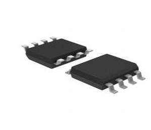
3.8V DC DC Voltage Regulator SWITCHING REGULATOR 1 Outputs 1.1MHz Tape & Reel (TR) SOT-23-6 Thin, TSOT-23-6


3.8V DC DC Voltage Regulator SWITCHING REGULATOR 1 Outputs 1.1MHz Tape & Reel (TR) SOT-23-6 Thin, TSOT-23-6
AP63205WU-7 is a switching voltage regulator. This article is going to explain pinout, features, applications, circuits, and more details about the AP63205WU-7 regulator.
What is AP63205WU-7?
The AP63205WU-7 is a 2A switching voltage regulator having a 3.8V to 32V input voltage range. A 125m high-side power MOSFET and a 68m low-side power MOSFET are fully integrated. To achieve high-efficiency step-down DC/DC conversion, a power MOSFET is used.
The AP63205WU-7 device is easily used by minimizing the external component count due to its adoption of peak current mode control along with its integrated compensation network.
AP63205WU-7 Pinout

AP63205WU-7 Pinout
AP63205WU-7 CAD Model

AP63205WU-7 Symbol

AP63205WU-7 Footprint

AP63205WU-7 3D Model
Specifications
- TypeParameter
- Factory Lead Time19 Weeks
- Mounting Type
The "Mounting Type" in electronic components refers to the method used to attach or connect a component to a circuit board or other substrate, such as through-hole, surface-mount, or panel mount.
Surface Mount - Package / Case
refers to the protective housing that encases an electronic component, providing mechanical support, electrical connections, and thermal management.
SOT-23-6 Thin, TSOT-23-6 - Operating Temperature
The operating temperature is the range of ambient temperature within which a power supply, or any other electrical equipment, operate in. This ranges from a minimum operating temperature, to a peak or maximum operating temperature, outside which, the power supply may fail.
-40°C~85°C TA - Packaging
Semiconductor package is a carrier / shell used to contain and cover one or more semiconductor components or integrated circuits. The material of the shell can be metal, plastic, glass or ceramic.
Tape & Reel (TR) - JESD-609 Code
The "JESD-609 Code" in electronic components refers to a standardized marking code that indicates the lead-free solder composition and finish of electronic components for compliance with environmental regulations.
e3 - Part Status
Parts can have many statuses as they progress through the configuration, analysis, review, and approval stages.
Active - Moisture Sensitivity Level (MSL)
Moisture Sensitivity Level (MSL) is a standardized rating that indicates the susceptibility of electronic components, particularly semiconductors, to moisture-induced damage during storage and the soldering process, defining the allowable exposure time to ambient conditions before they require special handling or baking to prevent failures
1 (Unlimited) - Terminal Finish
Terminal Finish refers to the surface treatment applied to the terminals or leads of electronic components to enhance their performance and longevity. It can improve solderability, corrosion resistance, and overall reliability of the connection in electronic assemblies. Common finishes include nickel, gold, and tin, each possessing distinct properties suitable for various applications. The choice of terminal finish can significantly impact the durability and effectiveness of electronic devices.
Matte Tin (Sn) - Function
The parameter "Function" in electronic components refers to the specific role or purpose that the component serves within an electronic circuit. It defines how the component interacts with other elements, influences the flow of electrical signals, and contributes to the overall behavior of the system. Functions can include amplification, signal processing, switching, filtering, and energy storage, among others. Understanding the function of each component is essential for designing effective and efficient electronic systems.
Step-Down - Number of Outputs1
- Voltage - Input (Max)
Voltage - Input (Max) is a parameter in electronic components that specifies the maximum voltage that can be safely applied to the input of the component without causing damage. This parameter is crucial for ensuring the proper functioning and longevity of the component. Exceeding the maximum input voltage can lead to electrical overstress, which may result in permanent damage or failure of the component. It is important to carefully adhere to the specified maximum input voltage to prevent any potential issues and maintain the reliability of the electronic system.
32V - Output Type
The "Output Type" parameter in electronic components refers to the type of signal or data that is produced by the component as an output. This parameter specifies the nature of the output signal, such as analog or digital, and can also include details about the voltage levels, current levels, frequency, and other characteristics of the output signal. Understanding the output type of a component is crucial for ensuring compatibility with other components in a circuit or system, as well as for determining how the output signal can be utilized or processed further. In summary, the output type parameter provides essential information about the nature of the signal that is generated by the electronic component as its output.
Fixed - Voltage - Input (Min)
Voltage - Input (Min) refers to the minimum voltage level that an electronic component requires to operate correctly. It indicates the lowest voltage that can be applied to the component while still allowing it to function as intended. If the input voltage falls below this specified minimum, the component may not perform properly or may fail to operate altogether. This parameter is critical for ensuring reliable operation and longevity of the device in electronic circuits.
3.8V - Analog IC - Other Type
Analog IC - Other Type is a parameter used to categorize electronic components that are integrated circuits (ICs) designed for analog signal processing but do not fall into more specific subcategories such as amplifiers, comparators, or voltage regulators. These ICs may include specialized analog functions such as analog-to-digital converters (ADCs), digital-to-analog converters (DACs), voltage references, or signal conditioning circuits. They are typically used in various applications where precise analog signal processing is required, such as in audio equipment, instrumentation, communication systems, and industrial control systems. Manufacturers provide detailed specifications for these components to help engineers select the most suitable IC for their specific design requirements.
SWITCHING REGULATOR - Output Configuration
Output Configuration in electronic components refers to the arrangement or setup of the output pins or terminals of a device. It defines how the output signals are structured and how they interact with external circuits or devices. The output configuration can determine the functionality and compatibility of the component in a circuit design. Common types of output configurations include single-ended, differential, open-drain, and push-pull configurations, each serving different purposes and applications in electronic systems. Understanding the output configuration of a component is crucial for proper integration and operation within a circuit.
Positive - Voltage - Output (Min/Fixed)
Voltage - Output (Min/Fixed) refers to the minimum fixed output voltage level that an electronic component, such as a voltage regulator or power supply, is designed to provide under specified load conditions. This parameter ensures that the device consistently delivers a reliable voltage that meets the requirements of the connected circuits or components. It is critical for applications where stable and predictable voltage is necessary for proper operation.
5V - Topology
In the context of electronic components, "topology" refers to the arrangement or configuration of the components within a circuit or system. It defines how the components are connected to each other and how signals flow between them. The choice of topology can significantly impact the performance, efficiency, and functionality of the electronic system. Common topologies include series, parallel, star, mesh, and hybrid configurations, each with its own advantages and limitations. Designers carefully select the appropriate topology based on the specific requirements of the circuit to achieve the desired performance and functionality.
Buck - Frequency - Switching
"Frequency - Switching" in electronic components refers to the rate at which a device, such as a transistor or switching regulator, turns on and off during operation. This parameter is crucial in determining the efficiency and performance of power converters, oscillators, and other circuits that rely on rapid switching. Higher switching frequencies typically allow for smaller component sizes but may require more advanced design considerations to manage heat and electromagnetic interference.
1.1MHz - Synchronous Rectifier
Synchronous rectification is a technique for improving the efficiency of rectification by replacing diodes with actively controlled switches, usually power MOSFETs or power bipolar junction transistors (BJT).
Yes - RoHS Status
RoHS means “Restriction of Certain Hazardous Substances” in the “Hazardous Substances Directive” in electrical and electronic equipment.
ROHS3 Compliant
AP63205WU-7 Features
VIN 3.8V to 32V
2A Continuous Output Current
0.8V ± 1% Reference Voltage
22µA Ultralow Quiescent Current
Switching Frequency
500 kHz: AP63200 and AP63201
1.1MHz: AP63203 and AP63205
Pulse Width Modulation (PWM) Regardless of Output Load
AP63201
Supports Pulse Frequency Modulation (PFM)
AP63200, AP63203, and AP63205
Up to 80% Efficiency at 1mA Light Load
Up to 88% Efficiency at 5mA Light Load
Fixed Output Voltage
3.3V: AP63203
5.0V: AP63205
Proprietary Gate Driver Design for Best EMI Reduction
Frequency Spread Spectrum (FSS) to Reduce EMI
Precision Enable Threshold to Adjust UVLO
Protection Circuitry
Overvoltage Protection
Cycle-by-Cycle Peak Current Limit
Thermal Shutdown
Lead-Free & Fully RoHS Compliant
Halogen and Antimony Free “Green” Device
AP63205WU-7 Functional Block Diagram
The following is AP63205WU-7 Functional Block Diagram:

AP63205WU-7 Functional Block Diagram
AP63205WU-7 Applications
Gaming Consoles
Flat Screen TV Sets and Monitors
Set-Top Boxes
Home Audio
Network Systems
Power Tools and Laser Printers
White Goods and Small Home Appliance
AP63205WU-7 Application Circuit
The following is the application circuit of AP63205WU-7:

AP63205WU-7 Application Circuit
AP63205WU-7 PCB Layout
The AP63205WU-7 PCB device works at 2A current load, so heat dissipation is a major concern in the layout of the PCB. 2oz copper for both the top and bottom layers is recommended.
Provide sufficient vias for the input and output capacitors’ GND side to dissipate heat to the bottom layer.
Make the bottom layer under the device the GND layer for heat dissipation. The GND layer should be as large as possible to provide a better thermal effect.
Place the VIN capacitors as close to the device as possible.
Place the feedback components as close to FB as possible.
The following is the PCB layout of AP63205WU-7 :

AP63205WU-7 PCB Layout
AP63205WU-7 Package Dimensions

AP63205WU-7 Package Dimensions
AP63205WU-7 Manufacturer
Diodes Incorporated delivers high-quality semiconductor products to the world’s leading companies in the consumer electronics, computing, communications, industrial, and automotive markets. They leverage their expanded product portfolio of discrete, analog, and mixed-signal products and leading-edge packaging technology to meet customers’ needs. Their broad range of application-specific solutions and solutions-focused sales, coupled with worldwide operations of 25 sites, including engineering, testing, manufacturing, and customer service, enables us to be a premier provider for high-volume, high-growth markets.
Trend Analysis
Datasheet PDF
- Datasheets :
What is the use of AP63205WU-7?
The AP63205WU-7 is easily used by minimizing the external component count due to its adoption of peak current mode control along with its integrated compensation network.
How does AP63205WU-7 work?
The AP63205WU-7 is a fixed output buck converter with Electromagnetic Interference (EMI) reduction. The converter features Frequency Spread Spectrum (FSS) with a switching frequency jitter of ±6%, which reduces EMI by not allowing emitted energy to stay in any one frequency for a significant period.
What is the nominal supply current of AP63205WU-7?
It is 22 µA.
 SI4463 Transceiver: Features, Pinout, and Datasheet
28 October 202111051
 ULN2004A Darlington Array: Pinout, Equivalent and Datasheet
29 November 20216792
 TIP36C Transistor: Equivalent, Datasheet, Test Circuit
29 November 20218718
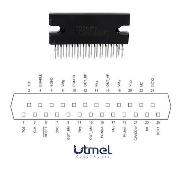 TB6560AHQ:PWM chopper-type stepping motor driver IC
17 April 20251498
 Designing with ATTINY13A: Datasheet, Pinout, and Motor Control Guide
31 January 202662
 TL071CD Operational Amplifier: Pinout, Specification, and Datasheet
16 August 20242949
![ATTINY84A-PU AVR series Microcontroller IC 8-Bit 20MHz[FAQ]: Datasheet, Features, and Pinout](https://res.utmel.com/Images/Article/889533d0-63dd-4ec6-8d21-6b346255db18.jpg) ATTINY84A-PU AVR series Microcontroller IC 8-Bit 20MHz[FAQ]: Datasheet, Features, and Pinout
ATTINY84A-PU AVR series Microcontroller IC 8-Bit 20MHz[FAQ]: Datasheet, Features, and Pinout18 March 2022643
 LT3045:High Performance Regulator
22 March 20224464
 Global Power Technology Authorized Distributor | UTMEL Electronics
21 November 20233837
 What is SPI (Serial Perripheral Interface)?
25 November 20214346
 Introduction to buck, boost, and buck-boost converters
28 September 202123770
 What is an Optical Sensor?
19 March 20216554
 Basic Introduction to Memristor
12 January 202111733
 Eight Internet of Things (IoT) Trends for 2022
08 April 20224966
 What is PWM "Dead Band"?
21 April 20226648
 How to read Resistors Color Code?
16 October 202522876
Diodes Incorporated
In Stock: 500
United States
China
Canada
Japan
Russia
Germany
United Kingdom
Singapore
Italy
Hong Kong(China)
Taiwan(China)
France
Korea
Mexico
Netherlands
Malaysia
Austria
Spain
Switzerland
Poland
Thailand
Vietnam
India
United Arab Emirates
Afghanistan
Åland Islands
Albania
Algeria
American Samoa
Andorra
Angola
Anguilla
Antigua & Barbuda
Argentina
Armenia
Aruba
Australia
Azerbaijan
Bahamas
Bahrain
Bangladesh
Barbados
Belarus
Belgium
Belize
Benin
Bermuda
Bhutan
Bolivia
Bonaire, Sint Eustatius and Saba
Bosnia & Herzegovina
Botswana
Brazil
British Indian Ocean Territory
British Virgin Islands
Brunei
Bulgaria
Burkina Faso
Burundi
Cabo Verde
Cambodia
Cameroon
Cayman Islands
Central African Republic
Chad
Chile
Christmas Island
Cocos (Keeling) Islands
Colombia
Comoros
Congo
Congo (DRC)
Cook Islands
Costa Rica
Côte d’Ivoire
Croatia
Cuba
Curaçao
Cyprus
Czechia
Denmark
Djibouti
Dominica
Dominican Republic
Ecuador
Egypt
El Salvador
Equatorial Guinea
Eritrea
Estonia
Eswatini
Ethiopia
Falkland Islands
Faroe Islands
Fiji
Finland
French Guiana
French Polynesia
Gabon
Gambia
Georgia
Ghana
Gibraltar
Greece
Greenland
Grenada
Guadeloupe
Guam
Guatemala
Guernsey
Guinea
Guinea-Bissau
Guyana
Haiti
Honduras
Hungary
Iceland
Indonesia
Iran
Iraq
Ireland
Isle of Man
Israel
Jamaica
Jersey
Jordan
Kazakhstan
Kenya
Kiribati
Kosovo
Kuwait
Kyrgyzstan
Laos
Latvia
Lebanon
Lesotho
Liberia
Libya
Liechtenstein
Lithuania
Luxembourg
Macao(China)
Madagascar
Malawi
Maldives
Mali
Malta
Marshall Islands
Martinique
Mauritania
Mauritius
Mayotte
Micronesia
Moldova
Monaco
Mongolia
Montenegro
Montserrat
Morocco
Mozambique
Myanmar
Namibia
Nauru
Nepal
New Caledonia
New Zealand
Nicaragua
Niger
Nigeria
Niue
Norfolk Island
North Korea
North Macedonia
Northern Mariana Islands
Norway
Oman
Pakistan
Palau
Palestinian Authority
Panama
Papua New Guinea
Paraguay
Peru
Philippines
Pitcairn Islands
Portugal
Puerto Rico
Qatar
Réunion
Romania
Rwanda
Samoa
San Marino
São Tomé & Príncipe
Saudi Arabia
Senegal
Serbia
Seychelles
Sierra Leone
Sint Maarten
Slovakia
Slovenia
Solomon Islands
Somalia
South Africa
South Sudan
Sri Lanka
St Helena, Ascension, Tristan da Cunha
St. Barthélemy
St. Kitts & Nevis
St. Lucia
St. Martin
St. Pierre & Miquelon
St. Vincent & Grenadines
Sudan
Suriname
Svalbard & Jan Mayen
Sweden
Syria
Tajikistan
Tanzania
Timor-Leste
Togo
Tokelau
Tonga
Trinidad & Tobago
Tunisia
Turkey
Turkmenistan
Turks & Caicos Islands
Tuvalu
U.S. Outlying Islands
U.S. Virgin Islands
Uganda
Ukraine
Uruguay
Uzbekistan
Vanuatu
Vatican City
Venezuela
Wallis & Futuna
Yemen
Zambia
Zimbabwe
![AP34063S8G-13]() AP34063S8G-13
AP34063S8G-13Diodes Incorporated
![AP3211KTR-G1]() AP3211KTR-G1
AP3211KTR-G1Diodes Incorporated
![AP3429KTTR-G1]() AP3429KTTR-G1
AP3429KTTR-G1Diodes Incorporated
![AP3429AKTTR-G1]() AP3429AKTTR-G1
AP3429AKTTR-G1Diodes Incorporated
![AP3012KTR-E1]() AP3012KTR-E1
AP3012KTR-E1Diodes Incorporated
![AP3015AKTR-G1]() AP3015AKTR-G1
AP3015AKTR-G1Diodes Incorporated
![PAM2306AYPKE]() PAM2306AYPKE
PAM2306AYPKEDiodes Incorporated
![AP3012KTR-G1]() AP3012KTR-G1
AP3012KTR-G1Diodes Incorporated
![AP1509-33SG-13]() AP1509-33SG-13
AP1509-33SG-13Diodes Incorporated
![AP5100WG-7]() AP5100WG-7
AP5100WG-7Diodes Incorporated


