Comparative Analysis of Si and SiC Devices for EV Traction Inverters
| Topics covered in this article: |
| Ⅰ. Simulation of Si and SiC devices on a Hybrid EV design |
| Ⅱ. Comparative Analysis between Si and SiC devices |
| Ⅲ. Conclusion |
The latest worldwide trends show that the world is rapidly shifting towards Electric Vehicles (EVs). As a result, major automobile companies are planning to move significant chunks of production to EVs.
Volvo plans to sell only EVs by 2030, Lotus by 2028, and General Motors by 2035. Also, countries like Japan plan to turn to EVs entirely by 2025.
One of the most critical components in EVs is traction inverters. It directly influences the driving experience, the battery range, and the vehicle's overall safety. The purpose of the traction inverter is to convert the DC from the EVs battery to AC to be used in the electric motor to drive the vehicle's propulsion system. There is increasing research in SiC-based power semiconductors to increase inverter efficiency, switching frequencies, maximum permissible junction temperature, and system power density. In the case of HEVs, highly integrated inverters cooled by the combustion engine's cooling circuit are a favorable solution, making an additional low-temperature power electronic cooling circuit dispensable.
This article is based on the IEEE research paper "Characterization and Scalable Modeling of Power Semiconductors for Optimized Design of Traction Inverters with Si and SiC-Devices." In this article, we aim to study the characteristics, compare the methods to calculate the power losses in thermal models and understand the power consumption and chip area required for different Si and SiC devices through the simulation of an NEDC vehicle with set parameters.
Some of the parameters for comparative analysis between Si and SiC devices are:
1. Power Loss
2. Device Modeling constraints
3. Minimum chip area for higher frequencies
Ⅰ. Simulation of Si and SiC devices on a Hybrid EV design
Firstly, we will explore a system simulation for a Hybrid EV traction inverter with Si and SiC devices with the final output.
This simulation used a vehicle power module with a package rating of tj(max) = 175 ◦C junction temperature and a typical combustion engine cooling fluid temperature of tf = 105 ◦C. The electrical machine determines the loss-influencing factors such as current, voltage, and power factor. Efficiency optimized speed–torque lookup tables are used as a fast method to define the operating conditions of the inverter. A minimal phase current operated machine for each dc-link voltage is considered without changing its electromagnetic design. The fluid-cooled pin-fin base plate has been proposed as a suitable power module cooling option for Hybrid and electric vehicles. Its thermal transition resistance of 19 mm2 KW has been used for the additional modeling.
The state-space representation of the Thermal Domain Transient Model with the Nonlinear Electrical Domain Loss Model as feedback was simulated with MATLAB/Simulink software.
A Vehicle Physics Model with gearshift was added to generate mission profiles for the HEV traction inverters from standardized drive cycles. The vehicle chosen for the simulations was a 2500-kg HEV–SUV with a gearbox-integrated permanent-magnet synchronous machine(PMSM) (32 poles, 500 Nm, 60 kW). Operating conditions for the simulation are:
1. Constant battery voltage:
a. 350 V for 650-V IGBTs
b. 700 V for 1200-V IGBTs
c. 700 V for 1200-V D-mode-SiC-JFETs
2. 10-kHz switching frequency
A brief overview of the simulation model structure is displayed below.

Figure.1 Simulation model for testing Si and SiC semiconductor traction inverters
The efficiency of the inverters and the electrical machine driving the new European drive cycle (NEDC) showed reduced losses of the SiC inverter, especially at partial load.

Figure.2 Inverter output to Efficiency graph for different power electronics technologies
The time domain simulation and transient modeling are done to test the power semiconductor's reliability and lifetime, considering the load profile and possible redesign of the chip area of the system. The application of the Rainflow-algorithm on the thermal chip time domain responses is a state-of-the-art procedure to count the thermal cycles of the package during the operation for an estimation of the lifetime.
This calculation showed no significant difference between the chip area optimized Si and SiC inverters. The simulation model also yields power losses from which the energy consumption for the semiconductor devices was calculated. The power losses for Si and SiC devices are:

Figure.3 Simulation output for various power electronics devices
Through this experiment of NEDC simulated driving, a possible reduction in energy loss of up to 70% for traction inverters with a 66% reduction in chip area using silicon carbide devices can be achieved as compared to silicon devices.
Ⅱ. Comparative Analysis between Si and SiC devices
Apart from the NEDC simulation, we also aim to study the characteristics and comparative analysis of different Si and SiC semiconductor devices:
1. Device Characterization
The laboratory setup for the investigation of switching behavior was set up with an external temperature controller. The gate driver has been designed to provide a configurable voltage between ±25 V with a maximum peak current of 1 A. The range of switching curves achieved for SiC-D-J-1200, SiC-E-J-1200, and SiC-EMOS-1200 devices is:

Figure.4 Half-bridge switching for SiC-D-J-1200 vs time for voltage, current and junction temperature

Figure.5 Half-bridge switching for SiC-E-J-1200 vs time for voltage, current and junction temperature

Figure.6 Half-bridge switching for SiC-E-MOS-1200 vs time for voltage, current and junction temperature
The turn-off behavior of all half-bridges is comparably fast, and there is no significant difference in the slopes.
A reverse recovery spike of the SiC-D-J-1200 at high currents and temperatures becomes significant during the turn-on of the SiC-body-diode. As a result, the device introduces a moderate ringing into the commutation loop due to steep current slopes, which reach the speed of the turn-off slope. The SiC-E-J1200 shows nearly no reverse recovery behavior due to the SiC JBS-diode. A flat voltage slope characterizes it during turn-on. This leads to significant switching losses. The SiC-E-MOS-1200 half bridge shows the fastest turn-on accompanied by the highest reverse recovery spike, leading to significant ringing in the commutation loop.
2. Thermal characteristics
The below figure shows the thermal characteristics of the device's differential area normalized on-state resistance. The D-mode SiC-JFET, SiC-MOSFET, and Si IGBTs show a flat thermal characteristic. At the same time, the E-mode SiC-JFET reveals a sharp increase in the resistance above 150 ◦ C. The bipolar Si diodes nearly reach an order of magnitude lower differential on-state resistance compared with the unipolar SiC-JBS-Diode, which is in the range of the SiC-FETs.
The voltage offset of the SiC-JBS-Diode decreases with temperature, as is with all the voltage offsets of the silicon devices. Therefore, the value of the SiC-JBS-Diode voltage offset is in the range below the 1200-V and above the 650-V silicon devices for the pictured temperature region.
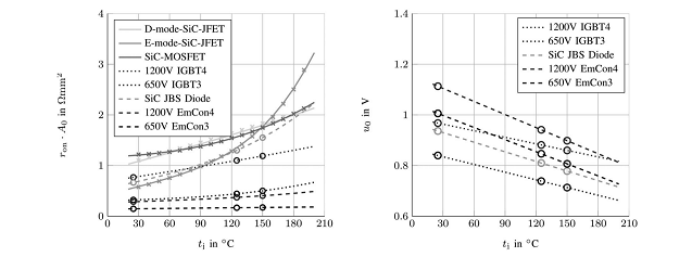
Figure.7 Resistance vs temperature and voltage vs temperature for different devices
The gate drive current varies in proportion to the chip area and parasitic inductance of the commutation loop varies inversely. Hence, comparing Si and SiC half bridges with the same chip area demonstrated five to ten times higher switching losses for the Si half bridges.
3. Heat Loss vs semiconductor chip areas

Figure.8 Power loss for different chip areas for different devices
The above figure shows the generated and dissipated heat at a set critical operating condition for different chip areas with 400-V dc-link voltage, 173-A peak phase current, 175 ◦C maximum junction temperature, and 10-kHz switching frequency. The results of the above experiment conclude that the minimum permissible chip area of the semiconductor device is given by the intersection of the generated and dissipated power over the chip area curve.
This minimum chip area was calculated numerically. In addition, the resulting minimum cumulated chip area of the traction inverter for a 60-kW electrical drivetrain component of an HEV has been calculated for different switching frequencies and battery voltages.

Figure.9 Chip area vs dc-link voltage at different switching frequencies and battery voltages
The Si inverters show an increase in minimum chip area for higher switching frequencies to dissipate the extra switching loss. In contrast, for SiC inverters, only a slight increase in chip area is needed. As far as comparison between same technology devices are concerned, Si-E-I-0650 technology performs better compared with Si-E-I-1200 for switching frequencies higher than 5 kHz. Also, the SiC-D-J-1200 and SiC-E-MOS-1200 show similar performance and surpass SiC-E-J-1200 due to utilization of the body diode.
Ⅲ. Conclusion
The simulated driving of the NEDC experiment presented in the research paper shows a 70% energy loss and 66% chip area reduction for traction inverters with SiC devices over Si power semiconductors. Through this article, we also presented the loss characterization of SiC semiconductors and dependence on dc-link voltage, current and junction temperature based on the same research paper.
 Analysis of Wide Bandgap Devices in Renewable Energy SystemsSaumitra Jagdale11 April 20234751
The article will describe the Analysis of Wide Bandgap Devices in Renewable Energy Systems.
Read More Role of Solar Energy in Wide-Band Gap Devices for Photovoltaic ApplicationsSaumitra Jagdale15 March 20244240
The enhancement of photovoltaic systems is closely linked to advancements in power semiconductor devices. Traditional Silicon-based power devices face challenges in meeting market demands for various applications such as EV, PV systems, and other high-power requirements. Presently, power device boasts enhanced efficiency, higher power density, increased blocking voltage, increased switching frequency, reduced cost, and improved reliability.
Read More Modeling, Modulation Analysis of Filter-Integrated Three-Switch Boost InverterRakesh Kumar, Ph.D.12 April 20234402
This article discusses the importance of inverters in energy conversion, the need for filters to eliminate harmonics that can cause system loss and circuit failure, two types of inverters, and an analysis of the three-switch boost inverter topology.
Read More An Analysis of Current-Source Inverters Using High-Frequency WBG SwitchesSaumitra Jagdale09 May 20234539
Hello everyone, welcome to the new post today.
Read More Three Phase Inverter - 180 Degree Conduction ModeRakesh Kumar, Ph.D.05 October 202319336
This technical article illustrates the working of the three phase power electronics inverter in the 180 degree conduction mode. The operation of the six thyristors and the associated waveforms are shown for easier understanding.
Read More
Subscribe to Utmel !


 Product
 Brand
Brand Articles
 Tools
Tools


