
 Product
 Brand
Brand Articles
 Tools
Tools
MMBT3906 PNP Switching Transistor: MMBT3906 Datasheet, Pinout, Alternatives


TRANS PNP 40V 0.2A SOT23
MMBT3906 is a PNP switching transistor in a SOT23 plastic package. This article will unlock more details about MMBT3906, including its pinout, datasheet, feature and so on... Welcome your RFQ!
MMBT3906 Pinout

MMBT3906 Pinout
MMBT3906 CAD Model
Symbol

MMBT3906 Symbol
Footprint

MMBT3906 Footprint
3D Model

MMBT3906 3D Model
MMBT3906 Datasheet
MMBT3906 Description
MMBT3906 is a PNP switching transistor in a SOT23 plastic package. NPN complement: MMBT3904.
MMBT3906 Feature
Collector current capability IC = −200 mA
Collector-emitter voltage VCEO = −40 V.
Emitter-Base Voltage: -5 V
Collector Current: -0.2 A
Collector Dissipation: 0.35 W
DC Current Gain (hfe): 100 to 300
Transition Frequency: 250 MHz
Noise Figure: 4 dB
Operating and Storage Junction Temperature Range: -55 to +150 °C
Package: SOT-23
MMBT3906 Application
• General switching and amplification.
MMBT3906 Alternatives
The alternatives for MMBT3906:
SMBT3906S
PMBT3906
2SA1366
2SA1518
2SA1519
2SA1520
Specifications
- TypeParameter
- Factory Lead Time4 Weeks
- Mounting Type
The "Mounting Type" in electronic components refers to the method used to attach or connect a component to a circuit board or other substrate, such as through-hole, surface-mount, or panel mount.
Surface Mount - Package / Case
refers to the protective housing that encases an electronic component, providing mechanical support, electrical connections, and thermal management.
TO-236-3, SC-59, SOT-23-3 - Surface Mount
having leads that are designed to be soldered on the side of a circuit board that the body of the component is mounted on.
YES - Number of Pins3
- Transistor Element Material
The "Transistor Element Material" parameter in electronic components refers to the material used to construct the transistor within the component. Transistors are semiconductor devices that amplify or switch electronic signals and are a fundamental building block in electronic circuits. The material used for the transistor element can significantly impact the performance and characteristics of the component. Common materials used for transistor elements include silicon, germanium, and gallium arsenide, each with its own unique properties and suitability for different applications. The choice of transistor element material is crucial in designing electronic components to meet specific performance requirements such as speed, power efficiency, and temperature tolerance.
SILICON - Collector-Emitter Saturation Voltage-400mV
- Current-Collector (Ic) (Max)200mA
- Number of Elements1
- hFEMin60
- Operating Temperature
The operating temperature is the range of ambient temperature within which a power supply, or any other electrical equipment, operate in. This ranges from a minimum operating temperature, to a peak or maximum operating temperature, outside which, the power supply may fail.
150°C TJ - Packaging
Semiconductor package is a carrier / shell used to contain and cover one or more semiconductor components or integrated circuits. The material of the shell can be metal, plastic, glass or ceramic.
Tape & Reel (TR) - Series
In electronic components, the "Series" refers to a group of products that share similar characteristics, designs, or functionalities, often produced by the same manufacturer. These components within a series typically have common specifications but may vary in terms of voltage, power, or packaging to meet different application needs. The series name helps identify and differentiate between various product lines within a manufacturer's catalog.
Automotive, AEC-Q101 - Published2009
- JESD-609 Code
The "JESD-609 Code" in electronic components refers to a standardized marking code that indicates the lead-free solder composition and finish of electronic components for compliance with environmental regulations.
e3 - Part Status
Parts can have many statuses as they progress through the configuration, analysis, review, and approval stages.
Active - Moisture Sensitivity Level (MSL)
Moisture Sensitivity Level (MSL) is a standardized rating that indicates the susceptibility of electronic components, particularly semiconductors, to moisture-induced damage during storage and the soldering process, defining the allowable exposure time to ambient conditions before they require special handling or baking to prevent failures
1 (Unlimited) - Number of Terminations3
- ECCN Code
An ECCN (Export Control Classification Number) is an alphanumeric code used by the U.S. Bureau of Industry and Security to identify and categorize electronic components and other dual-use items that may require an export license based on their technical characteristics and potential for military use.
EAR99 - Terminal Finish
Terminal Finish refers to the surface treatment applied to the terminals or leads of electronic components to enhance their performance and longevity. It can improve solderability, corrosion resistance, and overall reliability of the connection in electronic assemblies. Common finishes include nickel, gold, and tin, each possessing distinct properties suitable for various applications. The choice of terminal finish can significantly impact the durability and effectiveness of electronic devices.
Tin (Sn) - Terminal Position
In electronic components, the term "Terminal Position" refers to the physical location of the connection points on the component where external electrical connections can be made. These connection points, known as terminals, are typically used to attach wires, leads, or other components to the main body of the electronic component. The terminal position is important for ensuring proper connectivity and functionality of the component within a circuit. It is often specified in technical datasheets or component specifications to help designers and engineers understand how to properly integrate the component into their circuit designs.
DUAL - Terminal Form
Occurring at or forming the end of a series, succession, or the like; closing; concluding.
GULL WING - Peak Reflow Temperature (Cel)
Peak Reflow Temperature (Cel) is a parameter that specifies the maximum temperature at which an electronic component can be exposed during the reflow soldering process. Reflow soldering is a common method used to attach electronic components to a circuit board. The Peak Reflow Temperature is crucial because it ensures that the component is not damaged or degraded during the soldering process. Exceeding the specified Peak Reflow Temperature can lead to issues such as component failure, reduced performance, or even permanent damage to the component. It is important for manufacturers and assemblers to adhere to the recommended Peak Reflow Temperature to ensure the reliability and functionality of the electronic components.
260 - Time@Peak Reflow Temperature-Max (s)
Time@Peak Reflow Temperature-Max (s) refers to the maximum duration that an electronic component can be exposed to the peak reflow temperature during the soldering process, which is crucial for ensuring reliable solder joint formation without damaging the component.
40 - Base Part Number
The "Base Part Number" (BPN) in electronic components serves a similar purpose to the "Base Product Number." It refers to the primary identifier for a component that captures the essential characteristics shared by a group of similar components. The BPN provides a fundamental way to reference a family or series of components without specifying all the variations and specific details.
MMBT3906 - Pin Count
a count of all of the component leads (or pins)
3 - Qualification Status
An indicator of formal certification of qualifications.
Not Qualified - Configuration
The parameter "Configuration" in electronic components refers to the specific arrangement or setup of the components within a circuit or system. It encompasses how individual elements are interconnected and their physical layout. Configuration can affect the functionality, performance, and efficiency of the electronic system, and may influence factors such as signal flow, impedance, and power distribution. Understanding the configuration is essential for design, troubleshooting, and optimizing electronic devices.
SINGLE - Power Dissipation
the process by which an electronic or electrical device produces heat (energy loss or waste) as an undesirable derivative of its primary action.
250mW - Transistor Application
In the context of electronic components, the parameter "Transistor Application" refers to the specific purpose or function for which a transistor is designed and used. Transistors are semiconductor devices that can amplify or switch electronic signals and are commonly used in various electronic circuits. The application of a transistor can vary widely depending on its design and characteristics, such as whether it is intended for audio amplification, digital logic, power control, or radio frequency applications. Understanding the transistor application is important for selecting the right type of transistor for a particular circuit or system to ensure optimal performance and functionality.
SWITCHING - Gain Bandwidth Product
The gain–bandwidth product (designated as GBWP, GBW, GBP, or GB) for an amplifier is the product of the amplifier's bandwidth and the gain at which the bandwidth is measured.
250MHz - Polarity/Channel Type
In electronic components, the parameter "Polarity/Channel Type" refers to the characteristic that determines the direction of current flow or the type of signal that can be accommodated by the component. For components like diodes and transistors, polarity indicates the direction in which current can flow through the component, such as forward bias or reverse bias for diodes. For components like MOSFETs or JFETs, the channel type refers to whether the component is an N-channel or P-channel device, which determines the type of charge carriers that carry current through the component. Understanding the polarity or channel type of a component is crucial for proper circuit design and ensuring that the component is connected correctly to achieve the desired functionality.
PNP - Transistor Type
Transistor type refers to the classification of transistors based on their operation and construction. The two primary types are bipolar junction transistors (BJTs) and field-effect transistors (FETs). BJTs use current to control the flow of current, while FETs utilize voltage to control current flow. Each type has its own subtypes, such as NPN and PNP for BJTs, and MOSFETs and JFETs for FETs, impacting their applications and characteristics in electronic circuits.
PNP - Collector Emitter Voltage (VCEO)
Collector-Emitter Voltage (VCEO) is a key parameter in electronic components, particularly in transistors. It refers to the maximum voltage that can be applied between the collector and emitter terminals of a transistor while the base terminal is open or not conducting. Exceeding this voltage limit can lead to breakdown and potential damage to the transistor. VCEO is crucial for ensuring the safe and reliable operation of the transistor within its specified limits. Designers must carefully consider VCEO when selecting transistors for a circuit to prevent overvoltage conditions that could compromise the performance and longevity of the component.
-40V - Max Collector Current
Max Collector Current is a parameter used to specify the maximum amount of current that can safely flow through the collector terminal of a transistor or other electronic component without causing damage. It is typically expressed in units of amperes (A) and is an important consideration when designing circuits to ensure that the component operates within its safe operating limits. Exceeding the specified max collector current can lead to overheating, degradation of performance, or even permanent damage to the component. Designers must carefully consider this parameter when selecting components and designing circuits to ensure reliable and safe operation.
-200mA - DC Current Gain (hFE) (Min) @ Ic, Vce
The parameter "DC Current Gain (hFE) (Min) @ Ic, Vce" in electronic components refers to the minimum value of the DC current gain, denoted as hFE, under specific operating conditions of collector current (Ic) and collector-emitter voltage (Vce). The DC current gain hFE represents the ratio of the collector current to the base current in a bipolar junction transistor (BJT), indicating the amplification capability of the transistor. The minimum hFE value at a given Ic and Vce helps determine the transistor's performance and efficiency in amplifying signals within a circuit. Designers use this parameter to ensure proper transistor selection and performance in various electronic applications.
100 @ 10mA 1V - Current - Collector Cutoff (Max)
The parameter "Current - Collector Cutoff (Max)" refers to the maximum current at which a transistor or other electronic component will cease to conduct current between the collector and emitter terminals. This parameter is important in determining the maximum current that can flow through the component when it is in the cutoff state. Exceeding this maximum cutoff current can lead to malfunction or damage of the component. It is typically specified in the component's datasheet and is crucial for proper circuit design and operation.
50nA ICBO - Vce Saturation (Max) @ Ib, Ic
The parameter "Vce Saturation (Max) @ Ib, Ic" in electronic components refers to the maximum voltage drop across the collector-emitter junction when the transistor is in saturation mode. This parameter is specified at a certain base current (Ib) and collector current (Ic) levels. It indicates the minimum voltage required to keep the transistor fully conducting in saturation mode, ensuring that the transistor operates efficiently and does not enter the cutoff region. Designers use this parameter to ensure proper transistor operation and to prevent overheating or damage to the component.
400mV @ 5mA, 50mA - Voltage - Collector Emitter Breakdown (Max)
Voltage - Collector Emitter Breakdown (Max) is a parameter that specifies the maximum voltage that can be applied between the collector and emitter terminals of a transistor or other semiconductor device before it breaks down and allows excessive current to flow. This parameter is crucial for ensuring the safe and reliable operation of the component within its specified limits. Exceeding the maximum breakdown voltage can lead to permanent damage or failure of the device. Designers and engineers must carefully consider this parameter when selecting components for their circuits to prevent potential issues and ensure proper functionality.
40V - Transition Frequency
Transition Frequency in electronic components refers to the frequency at which a device can transition from one state to another, typically defining the upper limit of its operating frequency. It is a critical parameter in determining the speed and performance of active components like transistors and integrated circuits. This frequency is influenced by factors such as capacitance, resistance, and the inherent characteristics of the materials used in the component's construction. Understanding transition frequency is essential for optimizing circuit designs and ensuring reliable signal processing in various applications.
250MHz - Collector Base Voltage (VCBO)
Collector Base Voltage (VCBO) is the maximum allowable voltage that can be applied between the collector and base terminals of a bipolar junction transistor when the emitter is open. It is a critical parameter that determines the voltage rating of the transistor and helps prevent breakdown in the collector-base junction. Exceeding this voltage can lead to permanent damage or failure of the component.
-40V - Emitter Base Voltage (VEBO)
Emitter Base Voltage (VEBO) is a parameter used in electronic components, particularly in transistors. It refers to the maximum voltage that can be applied between the emitter and base terminals of a transistor without causing damage to the device. Exceeding this voltage limit can lead to breakdown of the transistor and potential failure. VEBO is an important specification to consider when designing circuits to ensure the proper operation and reliability of the components. It is typically provided in the datasheet of the transistor and should be carefully observed to prevent any potential damage during operation.
-6V - Max Junction Temperature (Tj)
Max Junction Temperature (Tj) refers to the maximum allowable temperature at the junction of a semiconductor device, such as a transistor or integrated circuit. It is a critical parameter that influences the performance, reliability, and lifespan of the component. Exceeding this temperature can lead to thermal runaway, breakdown, or permanent damage to the device. Proper thermal management is essential to ensure the junction temperature remains within safe operating limits during device operation.
150°C - Ambient Temperature Range High
This varies from person to person, but it is somewhere between 68 and 77 degrees F on average. The temperature setting that is comfortable for an individual may fluctuate with humidity and outside temperature as well. The temperature of an air conditioned room can also be considered ambient temperature.
150°C - Turn On Time-Max (ton)
Turn On Time-Max (ton) is a parameter in electronic components that refers to the maximum time it takes for a device to transition from an off state to an on state when a specific input signal is applied. This parameter is crucial in determining the speed and efficiency of the component in switching operations. A shorter turn-on time indicates faster response and better performance in applications where quick switching is required. It is typically specified in the component's datasheet and is important for designers to consider when selecting components for their circuits to ensure proper functionality and timing requirements are met.
70ns - Height1.1mm
- RoHS Status
RoHS means “Restriction of Certain Hazardous Substances” in the “Hazardous Substances Directive” in electrical and electronic equipment.
ROHS3 Compliant
Parts with Similar Specs
- ImagePart NumberManufacturerPackage / CaseVoltage - Collector Emitter Breakdown (Max)Max Collector CurrentTransition FrequencyCollector Emitter Saturation VoltagehFE MinPower DissipationMounting TypeView Compare
![MMBT3906,215]()
MMBT3906,215
TO-236-3, SC-59, SOT-23-3
40V
-200 mA
250 MHz
-400 mV
60
250 mW
Surface Mount
![FJV4114RMTF]()
TO-236-3, SC-59, SOT-23-3
-
100 mA
200 MHz
-
68
200 mW
Surface Mount
![FJV4110RMTF]()
TO-236-3, SC-59, SOT-23-3
40V
100 mA
-
-
100
200 mW
Surface Mount
![FJV4104RMTF]()
TO-236-3, SC-59, SOT-23-3
-
100 mA
200 MHz
-
68
200 mW
Surface Mount


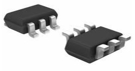
MMBT3906 Package

MMBT3906 Package
MMBT3906 Manufacturer
Nexperia is a dedicated global leader in Discretes, Logic and MOSFETs devices. This new company became independent at the beginning of 2017. Focused on efficiency, Nexperia produces consistently reliable semiconductor components at a high volume: 85 billion annually. The company's extensive portfolio meets the stringent standards set by the Automotive industry. And industry-leading small packages, produced in their own manufacturing facilities, combine power and thermal efficiency with best-in-class quality levels. Built on over half a century of expertise, Nexperia has 11,000 employees across Asia, Europe and the U.S. supporting customers globally.
Datasheet PDF
- Datasheets :
- PCN Assembly/Origin :
- PCN Packaging :
- PCN Design/Specification :
- RohsStatement :
Trend Analysis
How does a PNP transistor work as a switch?
For a PNP transistor, the Emitter potential must be positive with respect to the Base. ... With a positive signal applied to the base of the transistor it turns “ON” acting like a closed switch and maximum circuit current flows through the device.
What is PNP transistor used for?
PNP transistors are used in amplification circuits. PNP transistors are used in Darlington pair circuits. PNP transistors are used in robotic applications. PNP transistors to control current flow in heavy applications.
What is difference between PNP and NPN transistor?
An NPN transistor has a piece of P-type silicon (the base) sandwiched between two pieces of N-type (the collector and emitter). In a PNP transistor, the type of the layers are reversed. ... NPN and PNP transistors have very similar schematic symbols. The only difference is the direction of the arrow on the emitter.
.png) AD558: A Versatile Digital to Analog Converter for Precise Voltage Output
AD558: A Versatile Digital to Analog Converter for Precise Voltage Output06 March 2024450
 MC74HC4051A Analog Multiplexer: Pinout, Equivalent and Datasheet
14 February 20224080
 AD9371 300 MHz to 6 GHz Wideband RF Transceiver: Technical Deep Dive and Performance Review
13 March 2026322
 LIS2DW12TR Motion Sensor: Datasheet, Pinout, Application Hint
07 April 20225044
 TPS92630QPWPRQ1 LED Driver: Pinout, Manufacturer, and Datasheet
23 March 2022357
![CAP1188 Sensor: Diagram, Pinout, and Datasheet [Video&FAQ]](https://res.utmel.com/Images/Article/dff3f31a-bd56-4349-8550-62e74c3d5428.png) CAP1188 Sensor: Diagram, Pinout, and Datasheet [Video&FAQ]
CAP1188 Sensor: Diagram, Pinout, and Datasheet [Video&FAQ]04 May 20223674
 PIC18F46K22 Microcontroller: Features, Pinout, and Datasheet
27 October 20218321
 SN74LVC2G17DCKR Dual Schmitt-Trigger Buffer: Circuit, Pinout, and Datasheet
29 March 20223744
 Top 10 Popular Semiconductor Companies in 2025
25 December 202516250
 LDR/Light Dependent Resistor: Working Principle, Types and Applications
19 January 202633466
 Introduction to Flash Memory
31 October 20259718
 Essential Tips for Picking the Best Gas Sensor
15 July 20252966
 Manifold Absolute Pressure (MAP) Sensor: Working Principles, Structure, and Types
31 March 202548277
 Emerging Storage Technologies: MRAM, RRAM, and PCRAM
08 January 202616267
 What are the Differences Between Pull up and Pull down Resistors?
22 October 202539162
 Understanding Photodiodes: Working Principles and Applications - Part 2
24 May 20245146
Nexperia USA Inc.
In Stock: 45000
United States
China
Canada
Japan
Russia
Germany
United Kingdom
Singapore
Italy
Hong Kong(China)
Taiwan(China)
France
Korea
Mexico
Netherlands
Malaysia
Austria
Spain
Switzerland
Poland
Thailand
Vietnam
India
United Arab Emirates
Afghanistan
Åland Islands
Albania
Algeria
American Samoa
Andorra
Angola
Anguilla
Antigua & Barbuda
Argentina
Armenia
Aruba
Australia
Azerbaijan
Bahamas
Bahrain
Bangladesh
Barbados
Belarus
Belgium
Belize
Benin
Bermuda
Bhutan
Bolivia
Bonaire, Sint Eustatius and Saba
Bosnia & Herzegovina
Botswana
Brazil
British Indian Ocean Territory
British Virgin Islands
Brunei
Bulgaria
Burkina Faso
Burundi
Cabo Verde
Cambodia
Cameroon
Cayman Islands
Central African Republic
Chad
Chile
Christmas Island
Cocos (Keeling) Islands
Colombia
Comoros
Congo
Congo (DRC)
Cook Islands
Costa Rica
Côte d’Ivoire
Croatia
Cuba
Curaçao
Cyprus
Czechia
Denmark
Djibouti
Dominica
Dominican Republic
Ecuador
Egypt
El Salvador
Equatorial Guinea
Eritrea
Estonia
Eswatini
Ethiopia
Falkland Islands
Faroe Islands
Fiji
Finland
French Guiana
French Polynesia
Gabon
Gambia
Georgia
Ghana
Gibraltar
Greece
Greenland
Grenada
Guadeloupe
Guam
Guatemala
Guernsey
Guinea
Guinea-Bissau
Guyana
Haiti
Honduras
Hungary
Iceland
Indonesia
Iran
Iraq
Ireland
Isle of Man
Israel
Jamaica
Jersey
Jordan
Kazakhstan
Kenya
Kiribati
Kosovo
Kuwait
Kyrgyzstan
Laos
Latvia
Lebanon
Lesotho
Liberia
Libya
Liechtenstein
Lithuania
Luxembourg
Macao(China)
Madagascar
Malawi
Maldives
Mali
Malta
Marshall Islands
Martinique
Mauritania
Mauritius
Mayotte
Micronesia
Moldova
Monaco
Mongolia
Montenegro
Montserrat
Morocco
Mozambique
Myanmar
Namibia
Nauru
Nepal
New Caledonia
New Zealand
Nicaragua
Niger
Nigeria
Niue
Norfolk Island
North Korea
North Macedonia
Northern Mariana Islands
Norway
Oman
Pakistan
Palau
Palestinian Authority
Panama
Papua New Guinea
Paraguay
Peru
Philippines
Pitcairn Islands
Portugal
Puerto Rico
Qatar
Réunion
Romania
Rwanda
Samoa
San Marino
São Tomé & Príncipe
Saudi Arabia
Senegal
Serbia
Seychelles
Sierra Leone
Sint Maarten
Slovakia
Slovenia
Solomon Islands
Somalia
South Africa
South Sudan
Sri Lanka
St Helena, Ascension, Tristan da Cunha
St. Barthélemy
St. Kitts & Nevis
St. Lucia
St. Martin
St. Pierre & Miquelon
St. Vincent & Grenadines
Sudan
Suriname
Svalbard & Jan Mayen
Sweden
Syria
Tajikistan
Tanzania
Timor-Leste
Togo
Tokelau
Tonga
Trinidad & Tobago
Tunisia
Turkey
Turkmenistan
Turks & Caicos Islands
Tuvalu
U.S. Outlying Islands
U.S. Virgin Islands
Uganda
Ukraine
Uruguay
Uzbekistan
Vanuatu
Vatican City
Venezuela
Wallis & Futuna
Yemen
Zambia
Zimbabwe
![PMBT3904,215]() PMBT3904,215
PMBT3904,215Nexperia USA Inc.
![BC857C,215]() BC857C,215
BC857C,215Nexperia USA Inc.
![BC817-40,215]() BC817-40,215
BC817-40,215Nexperia USA Inc.
![BC807-40,215]() BC807-40,215
BC807-40,215Nexperia USA Inc.
![BC846B,215]() BC846B,215
BC846B,215Nexperia USA Inc.
![PMBT2222A,215]() PMBT2222A,215
PMBT2222A,215Nexperia USA Inc.
![PMBT2907A,215]() PMBT2907A,215
PMBT2907A,215Nexperia USA Inc.
![BC807-25,215]() BC807-25,215
BC807-25,215Nexperia USA Inc.
![PBSS4350Z,135]() PBSS4350Z,135
PBSS4350Z,135Nexperia USA Inc.
![BC847,215]() BC847,215
BC847,215Nexperia USA Inc.
