Product
 Brand
Brand Articles
 Tools
Tools
What are the Differences in the Copying Methods of Double-Sided and Multi-Layer PCBs?
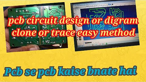
pcb print clone or trace circuit diagram design make new pcb circuit print
| Topics covered in this article: |
| Ⅰ. The specific steps of PCB copying |
| Ⅱ. Double-sided copying method |
| Ⅲ. Multilayer board copying method |
The technical realization of PCB copying is as simple as scanning the circuit board to be copied, recording the precise component positions, removing the components to create a bill of materials (BOM) and arrange for material procurement, and then sending the empty board to the plate manufacturing factory with the PCB file for production. After the PCB board is created, the purchased components are welded to it. The circuit board and debugging are then tested.
Ⅰ. The specific steps of PCB copying
1. Obtain a PCB, then write down the models, parameters, and locations of all the important components on the paper, paying particular attention to the direction of the diodes, triodes, and IC notch. It is advisable to use a digital camera to snap two images of the element's location. The sophistication of PCB circuit boards today is increasing. Some of the aforementioned diodes and triodes cannot be seen at all.
2. Take out the tin from the PAD hole and all of the multi-layer board components. After cleaning the PCB with alcohol, place it in the scanner. To produce a crisper image during scanning, the scanner needs to slightly increase the scanned pixels. Once the copper film is shiny, lightly buff the top and bottom layers with wet gauze paper, place them in the scanner, launch PHOTOSHOP, and scan the two layers in color. Remember that for the scanned image to be available, the PCB must be positioned both horizontally and vertically in the scanner.
3. Change the second image to black and white and make sure the lines are apparent. If not, repeat steps 3 and 4 to adjust the canvas's contrast and brightness such that the area covered with copper film and the area that isn't have a strong contrast. If it is obvious that the images were saved as the files TOP.BMP and BOT.BMP in the BMP format, if you find any problems with the graphics, you can also use PHOTOSHOP to repair and correct them.
4. Transfer two levels in PROTEL from the two BMP format files into their corresponding PROTEL format files. For instance, the positions of PAD and VIA after the two layers are nearly identical, demonstrating the effectiveness of the initial procedures. The third step should be repeated if there is any variance. Therefore, PCB copying is a task that requires patience because even a minor issue will have an impact on the copy's quality and degree of matching.
5. Change the TOP layer's BMP to TOP.
PCB, be sure to change it to the SILK layer (the yellow layer), after which you can draw a line on the TOP layer and, in the following step, position the device in accordance with the drawing. After drawing, delete the SILK layer, and repeat until all layers are drawn.
6. Import TOP.PCB and BOT.PCB into PROTEL and merge them into a single image.
7. Print the TOP LAYER and BOTTOM LAYER on the transparencies in a 1:1 ratio using a laser printer, then place the film on the PCB and check for errors. Upon confirmation, you are done.
A duplicate of the original board was created, however it was incomplete. Testing is also required to see if the clone board's electronic technical performance is identical to that of the original board. If so, it is effectively finished.
Remarks: If the board has multiple layers, it should be properly polished down to the inner layer while also copying the third through fifth processes. Of course, the names given to the graphics vary as well, and they should be chosen based on the number of layers. The double-sided board should typically be replicated. The multi-layer copy board should be extremely cautious and meticulous because it is much simpler than the multi-layer board and the multi-layer copy board is prone to improper alignment (the internal vias and non-conductive holes are prone to problems).
Ⅱ. Double-sided copying method
1. Scan the circuit board's upper and lower layers, then save two BMP images.
2. Launch Quickpcb2005, select "File," and then "Open Basemap" to open a scanned image. In order to see the pad, insert a pad by pressing PP, observe the line, and route, use PAGEUP to magnify the screen. Draw it again in this program like a kid would, then click "Save" to create a B2P file.
3. To view the scanned color image of a different layer, select "File" and "Open Basemap";

Figure. 1
4. To open the B2P file previously saved, once again click "File" and "Open." The freshly duplicated board is shown layered on top of this image; it is the same PCB board; the holes are in the same locations; however, the circuit connections are different. In order to just see the multi-layer vias, we disable the lines and silkscreens that reveal the top layer by selecting "Options" - "Layer Settings."
5.The vias on the top layer and the bottom layer image are both in the same location. We can once again trace the base layer like we did when we were younger. Once more, click "Save" to add the top and bottom layers of data to the B2P file.
6. Click "File" and "Export as PCB File", you can get a PCB file with two layers of data, you can re-modify the board or re-print the schematic diagram or send it directly to the PCB plate-making factory for production.
Ⅲ. Multilayer board copying method
A four-layer board can really be copied by using two double-sided boards, while a six-layer board can be copied by using three double-sided boards. The fact that we cannot see the internal circuitry makes numerous layers intimidating. How do we see the inner layers of a precision multi-layer board? – Layered
There are numerous methods for layering already, such as knife peeling and potion corrosion, however it is simple to divide the layers too much and lose data. We know from experience that sanding is the most precise.
After copying the top and bottom layers of the PCB, we often use sandpaper to remove the outer layer and reveal the inner layer. The PCB is typically laid out on a flat surface before the sandpaper is applied, rubbing the PCB evenly (If the board is small, you can also lay the sandpaper flat, hold the PCB with one finger and rub it on the sandpaper). In order for it to grind evenly, the object is to flatten.
The copper wire and copper skin should be repeatedly cleansed once the silk screen and green oil have been removed. Generally speaking, wiping the Bluetooth board only takes a few minutes, and wiping the memory stick takes around ten minutes. Of course, depending on your strength, it may take less time or a bit longer.
The most popular and affordable method of layering at the moment is grinding. We can look for an unused PCB. Although technically not difficult, grinding the board is a little monotonous. There is no need to worry about wearing the board into your fingertips; it just takes a little work.
In the PCB layout process, after the system layout is completed, the PCB diagram should be reviewed to see whether the system layout is reasonable and whether it can achieve the optimal effect.

Figure. 2
It can usually be investigated from the following aspects:
1. Whether the system layout can guarantee that the wiring is reasonable or ideal, whether it can guarantee that the wiring will operate reliably, and whether it can guarantee that the circuit will operate reliably. The direction of the signal as well as the power and ground network must be understood and planned for generally during the architecture.
2. Whether the printed board's dimensions match those of the processing drawing, whether it can satisfy the conditions of PCB manufacture, and whether a behavior mark is there. This issue need special consideration. Many PCB boards' circuit layouts and wirings are elegantly and sensibly constructed, but the proper positioning of the positioning connection is often overlooked, making it impossible for the specified circuit to be connected to other circuits.
3.The degree of incompatibility between elements in two- and three-dimensional space. Pay close attention to the device's real dimensions, particularly its height. The height typically cannot be greater than 3mm when soldering layout-free components.
4. The density and organization of the component layout, the neatness with which it is structured, and the completion of all layouts. When arranging components, it is important to take into account the overall density of the device layout so that the density is consistent, as well as the signal's direction, kind, and vulnerable locations.
5.Whether the plug-in board can be conveniently put into the device and whether the often replaced components can be simply replaced. The ease and dependability of the replacement and connection of the frequently replaced components should be guaranteed.
 UTMEL
UTMEL
We are the professional distributor of electronic components, providing a large variety of products to save you a lot of time, effort, and cost with our efficient self-customized service. careful order preparation fast delivery service
1. What is PCB copy board?
PCB copy board, also known as "circuit board clone", that is, under the premise of existing electronic products and circuit boards, reverse R&D technology is used to reversely analyze the circuit boards, and the PCB files and bills of materials of the original products will be reversed. (BOM) files, schematic files and other technical files and PCB silk screen production files are restored 1:1, and then use these technical files and production files for PCB board making, component welding, flying probe testing, and circuit board debugging, complete A complete reproduction of the original circuit board template. In layman's terms, it is to analyze a ready-made circuit board, copy its circuit direction and the use of electronic components completely, and then make it by yourself.
2. What is the difference between PCB copy board and PCB board?
PCB board is a manufactured product, which converts the designed drawing data (gerber file) into an actual product (PCB board).
The PCB copy board is to copy the PCB board made by others into a GerBer file. The PCB manufacturer needs this file to produce the PCB board. Copy board is copying others.
3. What are the ways to prevent PCB from being copied?
1. Sealing and painting the printed circuit board, this method can easily increase the difficulty of copying the board.
2. Chip grinding, the key to copying the board is to understand the chip. If you are familiar with all the chips on the printed board, it will be easier to copy the board. On the premise of not affecting the function of the chip, polish all the models of the chip. It is impossible to find the model of the chip, which greatly increases the difficulty for the copy board personnel.
3. Appropriately use some relatively unpopular and uncommon chips. If it is a very commonly used chip, even if the chip model cannot be checked, it is easy to infer the model of the chip based on the packaging and experience.
4. The PCB design adopts buried via and blind via technology, and the over-control is hidden in the board. It is difficult for the board copying personnel to infer the actual wiring according to the multi-layer circuits. However, the research and development cost of the buried via and blind via technology is relatively high, generally only Used in high-end products.
5. The processor selects chips with good encryption performance, high decryption difficulty and high security performance.
6. Add a self-destruction function chip to the hardware design, and add an anti-piracy function program to the software.
 Pull-Down Circuit Guide: Working Principle, Resistor Value, Circuit Design, and ApplicationsUTMEL26 June 202625
Learn how pull-down circuits work, how to choose a pull-down resistor value, and how to design reliable microcontroller inputs, MOSFET gates, reset pins, and sensor interfaces.
Read More HF PCB Circuit Design 10 QuestionsUTMEL16 March 20225340
Hello everyone, I am Rose. Today I want to give you a full explanation about PCB design. I Hope the following ten questions will give you a satisfied answer.
Read More How Many do You Know About the 12 Components Included in the Circuit Board?UTMEL12 February 20228758
We are lucky to live in an era where electronic devices are readily available. These electronic devices, on the other hand, come to us thanks to the incredible components on the circuit board, and we frequently wonder what makes electronic devices operate, how they achieve such massive success, and how they accomplish it. Electronic devices are incredible things; you can't see what's going on within them, but you can see what they're capable of. We'll talk about the wonders of PCBs and how to get past them to construct the circuit board in this article.
Read More![50 Frequently Asked Questions about PCB Layout [Q&A]](https://res.utmel.com/Images/Article/b5ce2a0a-d37c-4243-aff3-df7b2da2db0f.jpg "50 Frequently Asked Questions about PCB Layout [Q&A]") 50 Frequently Asked Questions about PCB Layout [Q&A]UTMEL16 November 20217148
50 Frequently Asked Questions about PCB Layout [Q&A]UTMEL16 November 20217148In the design of electronic products, PCB layout and routing is an important step, and the quality of PCB layout and routing will directly affect the performance of the circuit.
Read More An Overview of Development BoardUTMEL18 December 202515274
The development board is a circuit board used for embedded system development. Development boards are generally customized by embedded system developers according to development needs.
Read More
Subscribe to Utmel !
![SMH600PS24-EF-K]() SMH600PS24-EF-K
SMH600PS24-EF-KXP Power
![SDN4024100CX]() SDN4024100CX
SDN4024100CXSolaHD
![PEC550-12-074RD]() PEC550-12-074RD
PEC550-12-074RDBel Power
![CQB75-300S05-C]() CQB75-300S05-C
CQB75-300S05-CCincon
![ABC601-1T28]() ABC601-1T28
ABC601-1T28Bel Power
![CR00140-02]() CR00140-02
CR00140-02Trenz Electronic
![MS-10-12]() MS-10-12
MS-10-12TDK Lambda
![MDR-100-15]() MDR-100-15
MDR-100-15Advantech
![101188004]() 101188004
101188004Integrated Power Designs
![101191901]() 101191901
101191901Integrated Power Designs