Semiconductor Equipment Industry Research
1. TSMC raised its capital expenditure budget
1.1. Strong demand for expansion of downstream fabs
The scale of the global semiconductor market is growing against the trend, driving the demand for semiconductor special equipment: The semiconductor special equipment market is closely related to the prosperity of the semiconductor industry. Among them, chip manufacturing equipment is the field with the largest demand for the semiconductor special equipment industry, and the rapid development of downstream emerging industries is the maximum driving force of the semiconductor equipment industry.
Sales of semiconductor manufacturing equipment have grown strongly, and the semiconductor industry chain is expected to shift to China, which will become the largest market for semiconductor equipment: According to SEMI statistics, global semiconductor equipment sales in 2020 will reach a record high of US$71.2 billion, a year-on-year increase of 19%. In terms of regions, mainland China became the world's largest semiconductor equipment market for the first time, with sales increasing by 39% year on year to US$18.72 billion. Taiwan, the second-largest equipment market, held steady in 2020 at $17.15 billion after showing strong growth in 2019.
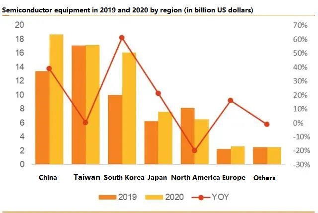
Semiconductor equipment in 2019 and 20 by region (in billion US dollars)
Since 2020 Q4, the shortage of chips has been serious, and it is expected to ease in 2022, and the demand for fab expansion is strong. The start of the high demand in the semiconductor industry is marked by the high demand for new energy vehicles in the second half of 2020. The tight chip production capacity has gradually spread from automotive chips to consumer chips. The demand for fab expansion is very strong. The main reasons for the lack of chips are as follows:
Before 2019, the demand for mobile phone chips was far greater than the demand for automobile chips. Many fabs transformed automobile chip production lines into mobile phone chip production lines, resulting in a significant reduction in global automobile chip production capacity. After the second half of 2020, the demand for new energy vehicles will increase, orders for automotive chips will increase significantly, and downstream fabs are completely unprepared.
The epidemic has caused a shock to the overall production capacity of the semiconductor industry.
Wafer production capacity is tight, downstream manufacturers have raised product prices: wafer shortage has become the norm, expanding from the 8-inch wafer field to the 12-inch field. At present, many chip foundries are operating at full capacity, but the production capacity is still tight and it is difficult to meet the huge demand OEM needs. As a result, domestic and foreign media and industry chains predict that the global chip shortage caused by at least the shortage of wafers will not begin to ease until the second half of 2022. Downstream chip makers are facing supply shortages due to wafer shortages, and have raised prices for this reason.
In response to the capacity gap, wafer manufacturers have expanded capacity: In response to the capacity gap, wafer manufacturers have expanded capacity. According to statistics, in 2020, a total of 12 wafer fabs will be constructed and put into operation in the mainland, with an additional capacity of 1.445 million wafers per month.
Wafer fab capacity expansion, new fab is expected to bring a lot of demand for semiconductor equipment: As of April 2021, some fab projects under construction in China have been counted, and the known investment scale is 95.72 billion yuan, which can provide a production capacity of 450,000-550,000 pieces/month. Semiconductor equipment is the largest investment in wafer fabs, accounting for about 75-80% of the total investment. It is expected that with the construction of wafer fab capacity expansion projects, there will be a large demand for semiconductor equipment.
1.2. The growth rate of downstream capital expenditure has increased, and the prosperity of semiconductor equipment has continued to rise
The semiconductor equipment industry is highly affected by the capital expenditure of downstream manufacturers and has a certain cyclical attribute. With the growth of downstream demand in recent years, the capital expenditure of the global semiconductor industry will reach US$73.2 billion in 2020, and the growth rate will change from negative to positive.
In 2020, TSMC's capital expenditure reached US$17.2 billion, and capital expenditure continue to expand in the next few years. According to TSMC's first-quarter conference call, it is expected that capital expenditure will increase to US$30 billion in 2021, and the capital expenditure in the next three years (21-23) will total 1,000 US dollars. US$100 million, of which 80% is used for advanced processes (3nm, 5nm, 7nm), 10% is used for advanced packaging and mask manufacturing, and 10% is used for specialty processes.
2. Sorting out the semiconductor industry chain
2.1. Sorting out the semiconductor industry chain
Semiconductors refer to materials with electrical conductivity between conductors and insulators at room temperature and are widely used in various electronic products. Semiconductor products can be subdivided into four categories: integrated circuits, discrete devices, optoelectronic devices, and sensors. They are widely used in 5G communications, computers, consumer electronics, network communications, automotive electronics, the Internet of Things, and other industries.
Special equipment is the basis of semiconductor production: the production process of various semiconductors mainly includes chip design, wafer manufacturing, packaging and testing, and other processes. Each production process needs to be designed and manufactured within the scope allowed by the corresponding special equipment technology. The technology of semiconductor special equipment is complex, and the technical parameters of the equipment and the stability of the operation play a crucial role in the efficiency, quality, and yield of semiconductor production.
From the perspective of the industry chain, the semiconductor industry chain involves supporting industries such as materials and equipment, chip design, wafer manufacturing and packaging and testing industries, and semiconductor product terminal application industries. Semiconductors represented by integrated circuits have a wide range of product applications, and the growth in demand from downstream industries is the core driving force for the rapid development of the semiconductor industry.
2.2. Semiconductor equipment carding
2.2.1. Proportion of each equipment investment
The semiconductor manufacturing process mainly includes three main links: silicon wafer manufacturing, wafer manufacturing, and packaging and testing. In mature markets, wafer manufacturing equipment accounts for about 80%, and inspection, packaging, silicon wafer manufacturing, and other (such as mask manufacturing) equipment account for about 8%, 6%, 3%, and 3%, respectively.

Wafer Processing Equipment Investment Proportion
The wafer manufacturing process is the most important asset in the production chain, and the investment in wafer manufacturing equipment accounts for about 80% of the total equipment investment. Among the investment in wafer processing equipment, lithography equipment investment accounts for up to 25%, followed by thin film deposition accounting for 15%, and the third is front-end testing equipment, etching equipment, and packaging equipment, accounting for 10%. Followed by packaging and testing equipment (8%), cleaning equipment (7%), ion implantation equipment (3%), and crystal growth (2%).
2.2.2. Lithography machine
The basic principle of the lithography machine: pass the high-energy laser light through the reticle, pass the circuit pattern on the reticle through the condenser lens (projection lens), reduce the image by one-sixteenth, and then image (image copy) on the pre-coating photoresist layer on the wafer.
Main manufacturers: The concentration of lithography machine manufacturers is high. Among the world's major companies, the Netherlands ASML can cover all grades of lithography machine products and is in a leading position in the world with the production of high-end lithography machines. Other well-known lithography machine manufacturers include Japan's Canon (CANON) and Japan's Nikon (NIKON).
2.2.3. Etching equipment
Basic principle: Etching is a process of selectively removing unwanted materials from the surface of a silicon wafer by chemical or physical methods, usually after development and inspection, in order to correctly replicate the mask pattern on the glue-coated silicon wafer.
There are two basic etching processes in semiconductor manufacturing, dry etching, and wet etching, among which dry etching is the most important method for etching devices in submicron size.
Dry etching, also known as plasma etching, refers to the use of a gaseous chemical etchant to physically or chemically react (or both) with material on the silicon wafer not covered by photoresist to remove the exposed surface material process.
Wet etching refers to the process of chemically removing the surface material of silicon wafers using liquid chemical reagents (acids, alkalis, solvents, etc.). Due to its limitations in line width control and etching directionality, it is currently only used for etching certain layers or cleaning residues on silicon wafers.
Main production enterprises: There are many manufacturers of silicon etching machines, mainly include Pan-Lin Semiconductor, Applied Materials, and Tokyo Electronics of Japan; Chinese manufacturers include China Micro Corporation, North Huachuang, etc. Among them, the medium etching machine of China Micro Corporation has entered the 5nm process.
2.2.4. Cleaning equipment
Cleaning equipment is very important semiconductor equipment and is critical to ensuring chip yield. It is widely used in all aspects of semiconductor production. Repeated cleaning is required in lithography, etching, deposition, and other processes to avoid impurities affecting chip yield and performance.
According to the process, cleaning equipment can be mainly divided into wet cleaning equipment and dry cleaning equipment. Among them, the wet cleaning route accounts for more than 90% of the number of chip manufacturing cleaning steps. The working principle of the wet cleaning equipment is as follows: using a specific chemical solution and deionized water, the surface of the wafer is cleaned without damage to remove particles, natural oxide layers, organic matter, metal contamination, and sacrificial layers in the wafer manufacturing process. Under the wet cleaning process route, it can be divided into single-chip cleaning, tank cleaning, combined cleaning, and batch rotary spray cleaning.
Main manufacturers: The global cleaning equipment market is highly concentrated, and Japan's SCREEN and TEL are the leading companies. Other manufacturers include SEMES, LAMRESEARCH, as well as domestic manufacturers Shengmei Semiconductor, Zhichun Technology, and North Huachuang.
2.2.5. Ion implantation equipment
Basic principle: An ion implanter is a device that implants specific species of ions into specific materials with specified parameters, and performs the core doping process. To make a semiconductor into a device and change its electrical properties, impurities must be doped, and an ion implanter is the standard equipment for performing the doping process.
Main manufacturers: The global IC ion implanter industry market is basically occupied by Applied Materials, Other major manufacturers include Axecelis in the United States, Sumitomo Heavy Industries in Japan, and Zhongkexin in China.
2.2.6. Glue coating and developing equipment
Basic principle: The glue coating and developing equipment is the glue coating, baking, and developing equipment used in conjunction with the lithography machine in the photolithography process, including the glue coating machine (SpinCoater), the developer, and the spray coating machine (SprayCoater). The glue coating and developing equipment and the lithography machine work online to form a matching wafer processing and lithography production line to complete the fine lithography process.
Applicator: Apply photoresist to the clean and dry wafer surface. The silicon wafer is fixed on a vacuum slide stage, a liquid photoresist is dropped on the center of the silicon wafer, and a uniform photoresist coating is obtained by rotating.
Developer: Dissolve the exposed area of the positive photoresist with the developer solution (the negative photoresist is the non-exposed area). Cool the silicon wafer to about 23°C (same temperature as the developer), and chemically react with the developer to dissolve the exposed area to form the designed three-dimensional pattern.
Glue sprayer: Coat photoresist on irregular surface wafers. By atomizing the photoresist into droplets, the photoresist droplets are blown out by nitrogen (N2) and sprayed onto the surface of the substrate or wafer, and the hot plate carrying the wafer evaporates the photoresist solvent by heating. The resin remains on the surface of the substrate or wafer, resulting in a relatively uniform photoresist coverage.
Main production enterprises: In the current global glue developing equipment market, Tokyo Electronics (TEL) of Japan is in a leading position, with a market share of 86%. In addition, SCREEN, SEMES, and other enterprises are also strong. In the domestic glue coating and developing equipment market, Xinyuan Micro, as the only local enterprise, has a market share of about 4%, TEL is about 91%, and SCREEN is 5%.
2.2.7. Thin film deposition equipment
Basic principle: The working principle of thin film deposition technology is to achieve a series of adsorption involving atoms through physical or chemical methods. The adatoms diffuse on the surface and coalesce in appropriate positions, and then gradually form a thin film and grow. At present, the thin film deposition equipment on the market is mainly divided into three types according to the process: ADL (Atomic Layer Deposition), PVD (Physical Vacuum Coating), and Chemical Vacuum Coating (CVD).
ALD technology: A method (technology) in which a deposition film is formed by alternately passing gas-phase precursor pulses into the reactor and chemically adsorbing and reacting on the deposition substrate. When precursors reach the surface of the deposition substrate, they chemisorb on its surface and undergo surface reactions. The atomic layer deposition reactor needs to be cleaned with an inert gas between precursor pulses.
CVD technology: The vapor containing the gaseous reactant or liquid reactant and other gases required for the reaction are introduced into the reaction chamber, and a chemical reaction occurs on the surface of the substrate to form a thin film.
PVD technology: Under vacuum conditions, arc discharge technology with low voltage and high current is used, and gas discharge is used to evaporate the target material and ionize both the evaporated material and the gas, and use the acceleration of the electric field to make the evaporated material and its reaction. The product is deposited on the workpiece.
Main manufacturers: In the international thin film deposition equipment market, there are mainly applied materials, Fanlin Semiconductor, TEL, and other manufacturers. In the domestic market, the main companies are NAURA and Shenyang Tuojing. Among them, NAURA covers three product lines of CVD, ALD, and PVD. while Shenyang Tuojing mainly focuses on CVD and ALD. Both NAURA and Shenyang Tuojing have technology nodes that are reached 14/28nm.
2.2.8. Pre-channel quantity testing equipment
Basic principle: The pre-quantity detection works according to the principles of optics and electron beams. It is used in the processing and manufacturing process of wafers. It is a physical and functional test to detect whether the processing parameters of the product after each step of the process have reached the level.
According to the test purpose, the front-end volume detection can be subdivided into measurement and detection. The measurement is mainly to measure the chip's film thickness, key dimensions, registration accuracy, and other material properties, such as film stress, doping concentration, and other material properties to ensure that it meets the parameter design requirements; and detection is mainly used to identify and locate products. Problems such as contamination of impurity particles on the surface, mechanical scratches, wafer pattern defects, etc.
There are many kinds of front-line measurement equipment, including ellipsometer, four-probe, thermal wave system, coherent detection microscope, optical microscope, scanning electron microscope, etc.
Main production enterprises: Due to the extremely high technical and financial barriers, the front-line measurement equipment industry has strong requirements for the research and development capabilities of companies in the industry. At present, the domestic and foreign markets are highly concentrated, and the leading companies in the international market mainly include KLA in the United States, HITACHI in Japan, and ONTO in the United States.
2.2.9. Packaged devices
Basic principle: The packaging process is not: dicing, chip loading, bonding, plastic packaging, deflashing, electroplating, printing, rib cutting and forming, visual inspection, finished product testing, packaging, and shipping. Correspondingly, the packaging equipment includes cutting and thinning equipment, dicing machine, placement machine, curing equipment, wire welding/bonding equipment, plastic packaging, rib cutting equipment, etc.
Main production companies: In the field of packaging equipment production, representative companies in the global market include Shinkawa, KAWASAKI in Japan, Besi in the Netherlands, and ASMPacific in Hong Kong, China. Other domestic packaging equipment manufacturers include CLP 45, Shenzhen Cuitao, Suzhou Acres, Dalian Jiafeng, Fushi Sanjia, etc.
2.2.10. Testing equipment
Basic principle: Inspection equipment refers to the equipment that quantitatively inspects the quality and performance of silicon wafers or wafers during the entire production process or after several key processes, including probe stations, testing machines, and sorting machines. Check whether the various properties of the product in the production process and after production meet the design requirements.
Semiconductor testing includes wafer acceptability testing (WAT), wafer inspection (CP), and finished product testing (FT). The wafer acceptability test is mainly used to monitor process stability, determine shipping standards, etc.; wafer inspection (CP) is to test some basic device parameters, such as threshold voltage, on-resistance, source-drain breakdown voltage, etc.; Finished Product Test (FT) is to test the function and electrical parameters of the packaged chip.
Main manufacturers: At present, the market concentration is high, showing a highly concentrated pattern. Well-known foreign companies, such as Teradyne, Cohu in the United States, and Advantest in Japan, occupy a leading position in the high-end market by virtue of their strong technology and brand advantages.
2.3. Competitive landscape of the global semiconductor industry chain
2.3.1. Global Semiconductor Equipment Market
In terms of revenue, most of the top ten semiconductor equipment companies in the world are American and Japanese companies. In terms of the overall semiconductor equipment market, American and Japanese companies have obvious advantages and high market concentration, with CR10 as high as 76.6%. Among the top ten semiconductor equipment companies by global revenue in 2020, there are four American companies, four Japanese companies, and two Dutch companies. Among them, there are four companies with revenue of more than 10 billion US dollars, namely American Applied Materials (AMAT), Netherlands ASML, American Lam Research (LamResearch), and Japan Tokyo Electron (TEL).
Etching, thin-film, testing, cleaning, and other fields have broken domestic blanks, and technological breakthroughs have been rapid. In recent years, Chinese enterprises have continued to increase investment and made key breakthroughs in technology, breaking the gaps in many fields. The market has begun to realize Chinese substitution. For example, the research and development of micro-etching machines has reached the technology node of 5nm; the thin film deposition equipment of North Huachuang and Tuojing has reached the technology node of 14/28nm; the cleaning equipment of Zhichun Technology has entered SMIC, Hua Hong, etc. The supply chain of the enterprise; the testing machines of Huafeng Measurement and Control have entered the supply chain of international packaging and testing leaders such as ASE and STMicroelectronics.
2.3.2. Competitive landscape of the global semiconductor industry chain
Globally, American and Japanese companies have obvious advantages in most areas of the entire semiconductor industry chain. Other countries and regions, such as Taiwan China, South Korea, and Europe, are developing well in some fields.
Specifically:
Chip design: Most of the leading companies in the chip design industry are American companies. There are mainly Qualcomm, Broadcom, MediaTek, Nvidia, etc.
Wafer manufacturing: The wafer manufacturing industry is highly concentrated, and TSMC's leading position is stable, with a market share of more than 50% in 2021Q1. Other companies such as Samsung in South Korea, GlobalFoundries in the United States, and UMC in Taiwan have a relatively high market share.
Packaging and testing: The CR10 of the packaging and testing industry in 2020 is 83.98%, and the industry is highly concentrated. There are mainly ASE in Taiwan, Amkor in the United States, PTI in Taiwan, and United Technologies in Singapore.
Semiconductor front-end equipment: American and Japanese companies have great advantages. Leading companies in this field include Dutch ASML, American AMAT, Japanese TEL, Japanese SCREEN, American Ketian, and South Korean SEMES.
Packaging and testing equipment: The packaging and testing equipment market is also highly concentrated to the head. In terms of test equipment, in 2019, Japan's Advantech and American Teradyne had a combined market share of 90%. In terms of packaging equipment, the main companies are Shinkawa, Kawasaki, and so on.
Materials: Among the many subdivided semiconductor material markets, American and Japanese companies are still dominant. In terms of silicon wafers, Japan's Shin-Etsu Chemical, Japan's SUMCO, Germany's Siltronic, and South Korea's LG are the main companies; in terms of target materials, Japan's JX Nippon Mining Metals and American Honeywell are the leading companies; in terms of CMP polishing materials, Dow Chemical, Japan's Fujimi and Japan's HinomotoKenmazai are the leading companies; in terms of photoresist, Japan's JSR, Japan's Shin-Etsu Chemical. and the United States' Dow Chemical are the leading companies; in terms of electronic special gases, American Air Chemicals and American Praxair. Japan's Dayo Nippon Acid and others are leading companies; in terms of photomasks, American Photronics, Japan's DNP, and Japan's Toppan account for more than 80% of the market.
1.What was the global semiconductor market revenue in 2021?
$583.5 billion
2.What is the estimated investment scale for a new fab in China?
95.72 billion yuan
3.What is the core driving force for the rapid development of the semiconductor industry?
downstream industries
4.What companies have obvious advantages in most areas of the entire semiconductor industry chain?
American and Japanese
 Modeling Wide Band-Gap Semiconductors for Enhanced PerformanceRakesh Kumar, Ph.D.31 January 20243439
The article delves into the challenges faced by silicon-based power electronic devices and highlights the potential of wide band-gap semiconductors. It also emphasizes the importance of modeling power semiconductor devices and provides insights into various models. For electrical energy conversion to be dependable and effective, power electronics and semiconductor device technologies are essential.
Read More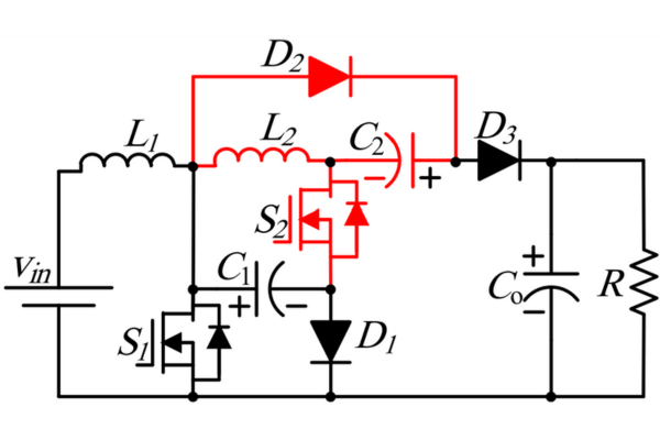 Optimizing Energy Management with Non-Isolated DC-DC ConvertersRakesh Kumar, Ph.D.04 February 20243080
The article classifies DC-DC converters and discusses the benefits and limitations of them. It proposes a modified DC-DC converter topology that combines the Cuk and Positive Output Super Lift Luo topologies to achieve a higher voltage gain with fewer components.
Read More ‘6G Networks’ - Pioneering the Next Era of Connectivity And InnovationRakesh Kumar, Ph.D.18 March 20243416
The article provides a comprehensive overview of the evolving landscape of mobile networks, the requirements that will shape the future of mobile communication, and the innovative technologies driving the transition to 6G.
Read More Review of IoT-Based Smart Home Security Systems- Part 1Rakesh Kumar, Ph.D.28 March 20243768
The article discusses the evolution of IoT-based smart home security systems, integrating advanced technologies like Raspberry Pi, PIR sensors, and voice recognition for enhanced user experience and efficiency.
Read More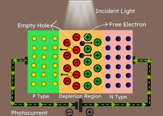 Understanding Photodiodes: Working Principles and Applications - Part 2Rakesh Kumar, Ph.D.24 May 20244454
The article provides a comprehensive overview of photodiodes, focusing on their operational principles, key factors affecting their efficiency, advantages, and disadvantages, and highlights their diverse applications.
Read More
Subscribe to Utmel !
![HOOKIT DISC 150MM X P120]()
![MAX6518UKP115 T]() MAX6518UKP115 T
MAX6518UKP115 TAnalog Devices
![98-0003-3052-6]()
![98-0003-3129-2]()
![98-0003-3046-8]()
![98-0003-3047-6]()
![2608596696]() 2608596696
2608596696Robert Bosch
![2608596731]() 2608596731
2608596731Robert Bosch
![2608630032]() 2608630032
2608630032Robert Bosch
![3M 987C diam 115, 36]()


 Product
 Brand
Brand Articles
 Tools
Tools


