Product
 Brand
Brand Articles
 Tools
Tools
What Is An Intrinsic Semiconductor?
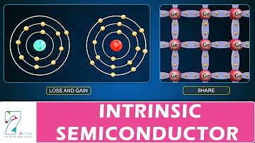
INTRINSIC SEMICONDUCTOR
Catalog
| I. General Introduction | |
| II. Conductivity principle | |
| III. Features | |
| 2. Temperature | |
| 3. Carriers | |
| IV. Applications | |
I. General Introduction
A single crystal made from a pure semiconductor through a certain process is called an intrinsic semiconductor. Two adjacent atoms of the intrinsic semiconductor share a pair of outermost electrons to form a covalent.

covalent bonds
Intrinsic semiconductors are pure semiconductors whose conductivity is mainly determined by the intrinsic excitation of the material. More generally speaking, a completely pure, impurity-free semiconductor is called an intrinsic semiconductor or I-type semiconductor. There are two forms of polycrystalline and single crystal in physical structure, and single crystal must be used to manufacture semiconductor devices. The purity of the semiconductor materials used to manufacture semiconductor devices must reach 99.9999999%. In the process of manufacturing semiconductor devices, the purity of materials will be further improved. Single crystals are not only highly pure, but also have no defects in the lattice structure. Only devices manufactured with such single crystals can guarantee the quality.
Typical intrinsic semiconductors include silicon (Si), germanium (Ge), and gallium arsenide (GaAs). Commonly used semiconductor materials are single crystal silicon (Si) and single crystal germanium (Ge). The so-called single-crystal refers to a crystal in which the atoms in the entire crystal are arranged neatly according to a certain rule.
II. Conductivity principle
Since the atoms of intrinsic semiconductors are connected by covalent bonds which have a strong binding force, at room temperature, only a small number of electrons can obtain enough energy through thermal motion (thermal excitation) to break free from the nucleus. The bond becomes a free electron, and at the same time, it leaves an empty position in the covalent bond, called an electron-hole. If a voltage is applied to both ends of the intrinsic semiconductor, the free electrons move directionally due to the action of the electric field. The directional movement of free electrons will fill the electron holes along the way. From a macro point of view, the electron holes are also moving in the opposite direction. Directional movement generates electron current, and electron-hole movement generates a current. This is the conductive principle of intrinsic semiconductors. Obviously, when the ambient temperature rises, the thermal movement intensifies, and the free electrons that break free from the covalent bond increase, and the electron holes also increase, so the conductivity is enhanced.
- Atoms are positively charged due to the loss of electrons, which can be understood as positively charged electron holes.
- When an intrinsic semiconductor conducts electricity, the electron current and electron-hole current move in opposite directions, and the current in an intrinsic semiconductor is the sum of the two currents.
- The particles that carry the charge are called carriers.
- There is only one type of carrier when the conductors conduct electricity: free electrons.
- There are two types of carriers when the Intrinsic semiconductor conduct electricity: free electrons and electron holes.
- The phenomenon that a semiconductor generates free electron and electron-hole pairs under thermal motion (thermal excitation) is called intrinsic excitation.
III. Features
1. Conductivity Features
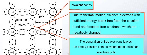
covalent bonds, free electrons, and electron holes
1.1 The covalent bond structure of the intrinsic semiconductor
Silicon and germanium are tetravalent elements. The four electrons on the outermost orbital of the atom are called valence electrons. They respectively form a covalent bond with the valence electrons of the surrounding four atoms. The valence electrons in the covalent bond are these atoms Shared by them, and bound by them. They form ordered crystals in space. The nucleus and inner electrons are usually regarded as a whole, which is called the inertial nucleus. The inertial nucleus has 4 units of positive charge, and the outermost layer has 4 A valence electron carries 4 units of negative charge. Therefore, the entire atom is electrically neutral.
1.2 Electron hole pair
Generally speaking, the valence electrons in the covalent bond are not completely as strong as the valence electrons in the insulator. If a certain amount of energy can be obtained from the outside (such as light, heating, electromagnetic field excitation, etc.), some valence electrons may break away from the common The valence bond becomes a free electron. This phenomenon is called intrinsic excitation (also called thermal excitation).
Theories and experiments show that at room temperature (T=300K), the valence electrons in the silicon covalent bond can be excited into free electrons as long as they obtain energy greater than the ionization energy EG (=1.1eV). The ionization energy of intrinsic germanium is even smaller. , Only 0.72eV.
When a valence electron in a covalent bond is forced to break free from the bondage of the nucleus and become a free electron, a vacant position is left in the covalent bond, called an "electron-hole". When an electron-hole appears, The valence electron of the adjacent atom is easier to leave the covalent bond where it is located and fill the hole to make a new electron-hole appear in the covalent bond where the valence electron was originally located. This electron-hole may be filled by the valence electron of the neighboring atom. New electron holes appear again. The movement of valence electrons to fill electron holes is equivalent to the movement of positively charged holes in both form and effect, and the direction of movement is opposite to the direction of movement of valence electrons. In order to distinguish it from free electrons This kind of movement is called cavity movement, and the cavity is regarded as a kind of carrier with a punctual load.
When free electrons encounter holes in the process of movement, they may be filled in to restore a covalent bond, and at the same time, an "electron-hole" pair disappears. This reverse process is called "recombination". Under certain temperature conditions, when the number of generated "electron-hole pairs" and the compound "electron-hole pairs" are equal, a relative balance is formed. This relative balance belongs to dynamic equilibrium. When dynamic equilibrium is accomplished, "electron-hole pairs" maintain a certain number.
It can be seen that there are two types of carriers, free electrons, and holes, in semiconductors, while there is only one type of free electron carrier in metal conductors. This is also the difference between semiconductors and conductors.
2. Temperature
1. Due to thermal motion, valence electrons with sufficient energy break free from the bondage of covalent bonds and become free electrons, which are negatively charged.
2. The higher the temperature is, the more electrons will break free. The higher the concentration of free electron and hole pairs (more carriers), and the higher the conductivity.
3. When the thermodynamic temperature is 0K (minus 273℃), it does not conduct electricity
4. The conductivity of intrinsic semiconductors has a lot to do with temperature.
3. Carriers
The particles that carry charge are called carriers. Intrinsic semiconductors have two types of carriers, free electrons, and electron holes.
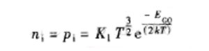
The formula of carrier concentration
- ni and pi represent the concentration of free electrons and holes, respectively
- T is the thermodynamic temperature
- k is the Paltzmann constant (8.63 * 10 ^ -5 eV/K)
- EGO is the energy required to break the covalent bond at zero degrees of thermodynamics (1.21 eV for silicon)
- K1 is a constant related to the effective mass and effective energy level density of semiconductor materials
IV. Applications
Intrinsic semiconductors do not contain impurities, have poor conductivity, and are greatly affected by temperature. Because of their large temperature-affected properties, they are often used as heat-sensitive and off-sensitive devices, which is also the cause of the poor temperature stability of semiconductor devices. Why should semiconductors be made into intrinsic semiconductors with poor conductivity? To make the conductivity of the materials controllable.
The electrons in the conduction band fall into the electron holes, causing the electron-hole pairs to disappear, which is called recombination. The energy generated during recombination is released in the form of electromagnetic radiation (photon emission) or thermal vibration of the lattice (phonon emission). At a certain temperature, the generation and recombination of electron-hole pairs exist at the same time and reach a dynamic equilibrium. At this time, the intrinsic semiconductor has a certain carrier concentration and thus a certain electrical conductivity. Heating or light will cause the semiconductor to be thermally or lightly excited, thereby generating more electron-hole pairs. At this time, the carrier concentration increases, and the conductivity increases. Semiconductor devices such as semiconductor thermistors and photoresistors are made according to this principle.
In practical applications, intrinsic germanium single crystals (required that the residual impurity concentration is less than 1010cm-3.) can be made into high-energy particle detectors, which are widely used in scientific research, geological prospecting, and medicine. Another example is silicon photodetectors made of highly pure near intrinsic silicon crystals, which have important applications in optical engineering.
The conductivity of intrinsic semiconductors at room temperature is small, and the carrier concentration is sensitive to temperature changes, so it is difficult to control semiconductor characteristics, so there are not many practical applications.
 UTMEL
UTMEL
We are the professional distributor of electronic components, providing a large variety of products to save you a lot of time, effort, and cost with our efficient self-customized service. careful order preparation fast delivery service
What are the properties of intrinsic semiconductor?
1)materials in pure form show the property of semiconductor are called intrinsic semiconductor. 2)the number of free electrons in the conduction band is equal to the number of holes in the valence bond. 3)Its electrical conductivity is low. 4)Its electrical conductivity depends on temperature only.
Is Aluminium an intrinsic semiconductor?
Dopants that contribute mobile electrons are called donor impurities; those that cause holes to form are acceptor impurities. Undoped semiconductor material is called intrinsic semiconductor material. Certain chemical compounds, including gallium arsenide, indium antimonide, and aluminum phosphide are semiconductors.
How many types of intrinsic semiconductors are there?
Semiconductors fall into two broad categories: Intrinsic semiconductors are composed of only one kind of material; silicon and germanium are two examples. These are also called “undoped semiconductors” or “i-type semiconductors.
 Modeling Wide Band-Gap Semiconductors for Enhanced PerformanceRakesh Kumar, Ph.D.31 January 20243551
The article delves into the challenges faced by silicon-based power electronic devices and highlights the potential of wide band-gap semiconductors. It also emphasizes the importance of modeling power semiconductor devices and provides insights into various models. For electrical energy conversion to be dependable and effective, power electronics and semiconductor device technologies are essential.
Read More Optimizing Energy Management with Non-Isolated DC-DC ConvertersRakesh Kumar, Ph.D.04 February 20243207
The article classifies DC-DC converters and discusses the benefits and limitations of them. It proposes a modified DC-DC converter topology that combines the Cuk and Positive Output Super Lift Luo topologies to achieve a higher voltage gain with fewer components.
Read More ‘6G Networks’ - Pioneering the Next Era of Connectivity And InnovationRakesh Kumar, Ph.D.18 March 20243546
The article provides a comprehensive overview of the evolving landscape of mobile networks, the requirements that will shape the future of mobile communication, and the innovative technologies driving the transition to 6G.
Read More Review of IoT-Based Smart Home Security Systems- Part 1Rakesh Kumar, Ph.D.28 March 20243954
The article discusses the evolution of IoT-based smart home security systems, integrating advanced technologies like Raspberry Pi, PIR sensors, and voice recognition for enhanced user experience and efficiency.
Read More Understanding Photodiodes: Working Principles and Applications - Part 2Rakesh Kumar, Ph.D.24 May 20245033
The article provides a comprehensive overview of photodiodes, focusing on their operational principles, key factors affecting their efficiency, advantages, and disadvantages, and highlights their diverse applications.
Read More
Subscribe to Utmel !
![110541]() 110541
110541Essentra Components
![T30UXIA-806639]() T30UXIA-806639
T30UXIA-806639Banner Engineering
![T30UXIA-806638]() T30UXIA-806638
T30UXIA-806638Banner Engineering
![WBWS633731-2OZ]() WBWS633731-2OZ
WBWS633731-2OZSRA Soldering
![FLS312-4G]() FLS312-4G
FLS312-4GSRA Soldering
![MCC-105EA]() MCC-105EA
MCC-105EAMicro Care
![110170]() 110170
110170Brady Corporation
![MAX6626PMTT]() MAX6626PMTT
MAX6626PMTTAnalog Devices
![110302]() 110302
110302Alpha Wire
![TCA355GGEGXT]() TCA355GGEGXT
TCA355GGEGXTInfineon