What is SMT (Surface Mount Technology)?

SMT PCB Assembly Process | Surface Mount Technology Manufacturing Process
Catalog |
Ⅰ SMT concept explanation
SMT (Surface Mount Technology) usually refers to a kind of electronic assembly technology that uses automated assembly equipment to mount and solder miniature surface-mounted components (SMC/SMD, collectively referred to as sheet components) directly onto the surface of printed circuit boards (PCBs) or other substrate surfaces at specified locations.
The standard in the electronics industry refers to SMT (Surface Mount Technology) as surface mount technology, which is an important part of modern electronic product advanced manufacturing technology.
Under normal circumstances, the electronic products we use are designed by PCB plus various capacitors, resistors, and other electronic components according to the designed circuit diagram, so electrical appliances need various SMT processing techniques to process.
Ⅱ Development Trends of Surface Mount Technology
The first stage (1960-1975): miniaturization, hybrid integrated circuits (thick film circuits); calculators, quartz watches, radios.
The second stage (1976-1985): miniaturization, enhanced circuit functions, SMT automation equipment, a large number of cameras, video recorders, digital cameras.
The third stage (1986-1995): highly integrated, reduce costs, improve product cost performance <PC, NB>
Current stage (1995-present): micro-assembly, high-density assembly, three-dimensional assembly <intelligent high-end electronic products (PDA, server).
The general trend of SMT development is that electronic products are becoming more and more powerful, smaller and smaller in size, lower and lower in price, and the speed of replacement is getting faster and faster.
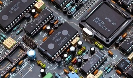
Surface mount components
The miniaturization of electronic products has led to higher and higher integration of semiconductor integrated circuits, and the pin spacing of SMC/SMD and IC has become shorter and shorter. The pin spacing has been reduced from a fine pitch of 0.3mm to 0.1mm.
Lead-free solders have become an inevitable trend to replace tin-lead solders. Countries and areas such as the European Union, the United States, and Japan have completely banned the use of lead, including banning the import of lead-containing electronic products. Electronic assembly is developing in the direction of lead-free conversion, and lead-free assembly is the inevitable trend of SMT development.
In terms of component technology: BGA, CSP, and FP (FlipChip) devices have become more widely used, and the technology has gradually matured. WLP is moving towards the semiconductor industry stage.
Technology status: Since the 1990s, electronic products using through-hole insertion technology have been declining at an annual rate of 11%, while the types of electronic products using SMT have been increasing at a rate of 8%.
Ⅲ SMT basic process
Solder paste printing --> parts placement --> reflow soldering --> AOI optical inspection --> maintenance --> sub-board.

SMT process
Electronic products are pursuing miniaturization, and the previously used perforated plug-in components can no longer be reduced. Electronic products have more complete functions, and the integrated circuits (ICs) used no longer have perforated components, especially large-scale, highly integrated ICs, which have to use surface mount components. With mass production of products and automation of production, the factory must produce high-quality products with low cost and high output to meet customer needs and strengthen market competitiveness. It is conceivable that when the production processes of international CPU and image processing device manufacturers such as Intel and AMD have advanced to more than 20 nanometers, the development of surface assembly technology such as SMT is also a necessity.
The advantages of SMT processing
High assembly density, small size, and lightweight. The volume and weight of the patch component are only about 1/10 of the traditional plug-in component. After SMT is generally adopted, the volume of electronic products is reduced by 40% to 60%, and the weight is reduced by 60% to 80%.
High reliability and strong anti-vibration ability.
The defect rate of solder joints is low.
Good high-frequency characteristics.
Reduce electromagnetic and radio frequency interference. It is easy to realize automation and improve production efficiency.
Reduce costs by 30%~50%. Save materials, energy, equipment, manpower, time, etc.
SMT Process
The basic process components of SMT include screen printing (or dispensing), mounting (curing), reflow soldering, cleaning, inspection, and rework.
1. Screen printing: Its function is to print solder paste or patch glue onto the PCB pads to prepare for the soldering of components. The equipment used is a screen printing machine, located at the forefront of the SMT production line.
2. Dispensing: It is to drop the glue onto the fixed position of the PCB board, and its main function is to fix the components on the PCB board. The equipment used is a glue dispenser, located at the forefront of the SMT production line or behind the testing equipment.
3. Mounting: Its function is to accurately mount the surface mount components to the fixed position of the PCB. The equipment used is a placement machine, located behind the screen printing machine in the SMT production line.
4. Curing: Its function is to melt the patch glue so that the surface assembly components and the PCB board are firmly bonded together. The equipment used is a curing oven, located behind the placement machine in the SMT production line.
5. Reflow soldering: Its function is to melt the solder paste so that the surface assembly components and the PCB board are firmly bonded together. The equipment used is a reflow oven, located behind the placement machine in the SMT production line.
6. Cleaning: Its function is to remove the solder residues such as flux that are harmful to the human body on the assembled PCB board. The equipment used is a washing machine, and the location may not be fixed, it may be online or offline.
7. Inspection: Its function is to inspect the welding quality and assembly quality of the assembled PCB board. The equipment used includes magnifying glass, microscope, online tester (ICT), flying probe tester, automatic optical inspection (AOI), X-RAY inspection system, functional tester, etc. The location can be configured in a suitable place on the production line according to the needs of the inspection.
8. Rework: Its function is to rework the PCB boards that have failed to detect faults. The tools used are soldering irons, rework stations, etc. Configured at any position in the production line.
Ⅳ Mounting process
Single-sided mount
Incoming inspection => silk screen solder paste (point patch glue) => mounting => drying (curing) => reflow soldering => cleaning => inspection => rework
Double-sided mount
A: Incoming inspection => PCB A-side silk-screen solder paste => mounting PCB B-side silk-screen solder paste => mounting => Drying => Reflow soldering ( It is best to only apply to side B => cleaning => inspection => rework).
B: Incoming inspection => PCB's A side silk screen solder paste => mounting => Drying (curing) => A side reflow soldering => Cleaning => Turnover = PCB's B side point SMD glue => mounting => curing => B surface wave soldering => cleaning => inspection => rework)
This process is suitable for reflow soldering on the A-side of the PCB and wave soldering on the B-side. This process should be used when only SOT or SOIC (28) pins are used in the SMD assembled on the B side of the PCB.
Single-sided mixed process
Incoming inspection => PCB A-side silkscreen solder paste => mounting => drying (curing) => reflow soldering => cleaning => plug-in => wave soldering => cleaning => inspection = > Rework
Double-sided mixed process
A: Incoming inspection => PCB's B side patch glue => mounting => curing => flipping => PCB A side plug-in => wave soldering => cleaning => inspection => rework
Paste first, insert later, suitable for situations where there are more SMD components than separate components
B: incoming inspection => PCB A-side plug-in (pin bending) => flipboard => PCB B-side point SMD adhesive => mounting => curing => flipboard => wave soldering => cleaning => testing => rework
Insert first, then paste, suitable for the situation where there are more separate components than SMD components
C: Incoming inspection => PCB A side silk screen solder paste => Patch => Drying => Reflow soldering => Plug-in, pin bending => Turnover => PCB side B point patch glue => mounting => curing => flipping => wave soldering => cleaning => inspection => rework
A side mixed, B side mounted.
D: Incoming inspection => PCB's B side point patch glue => mounting => curing => flip board => PCB's A side silk screen solder paste => mounting => A side reflow soldering => plug-in => B-side wave soldering => cleaning => inspection => rework A-side mixed assembly, B-side mounting.
First mount on both sides of SMD, reflow soldering, then inserting, wave soldering
E: Incoming inspection => PCB's B side silk screen solder paste (point patch glue) => mounting => drying (curing) => reflow soldering = > Flip board => PCB A-side silk screen solder paste => mounting => Drying = Reflow soldering 1 (partial soldering can be used) => Plug-in => Wave soldering 2 (If there are few inserted components, manual soldering can be used) => Cleaning => Inspection => Rework
A-side mounting and B-side mixed mounting.
1. What is SMT technology?
Surface mount technology

Surface mount technology (SMT) allows for the creation of customized electronic circuits by mounting individual components to a printed circuit board.
2. What is the difference between SMD and SMT?
The difference between SMD and SMT is that SMD (surface mount device) refers to an electronic component that is mounted on a PCB. In contrast, SMT (surface mount technology) relates to the method used to place electronic components on a printed circuit board.
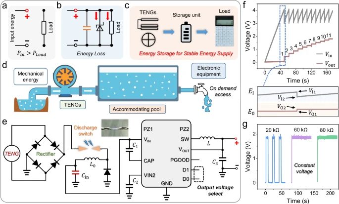 Improving the Energy Conversion Efficiency of Triboelectric NanogeneratorsSaumitra Jagdale19 November 20242903
There is a huge growth in demand for self-sustaining electronic devices, as the traditional power-generating devices fail in remote and harsh environments due to the periodic requirement of battery changes. Also, these devices are frequency specific; some work only in high frequency and some in low frequency. Triboelectric nanogenerators (TENGs) provide a promising solution by efficiently converting mechanical energy into electricity as they are versatile, compact, and cheap, making them a popular choice.
Read More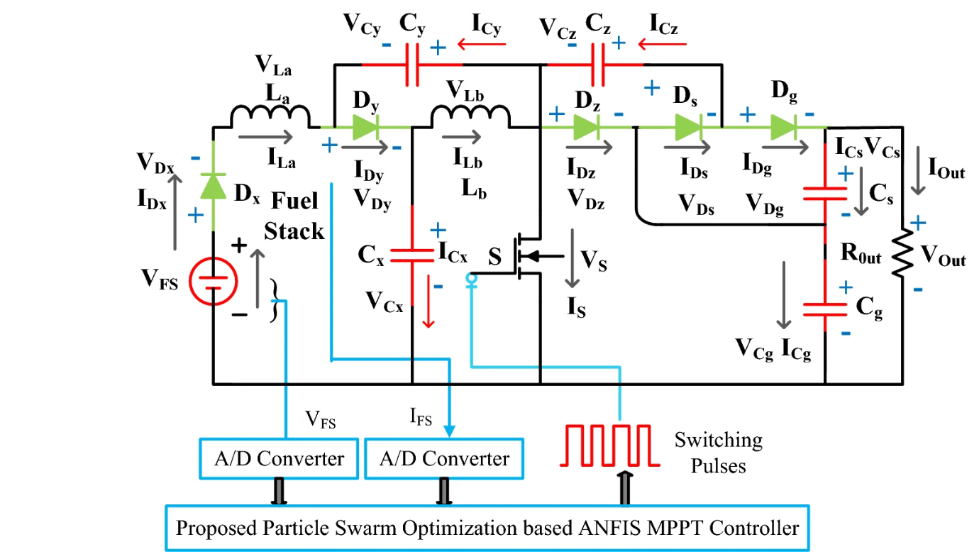 Methodologies for Increasing Efficiency of Fuel Stack Technology for Energy GenerationSaumitra Jagdale19 November 20242894
Presently, power companies are moving towards renewable energy systems. Conventional energy sources are more expensive because they require a vast network to be maintained and huge human resources. Also, they harm the environment by releasing several harmful gases. As the industry’s focus shifts toward renewable energy sources, energy systems powered by Proton Exchange Membrane Fuel Stacks (PEMFS) are gaining traction.
Read More Reconfigurable Antennas: Improving Efficiency in Modern CommunicationRakesh Kumar, Ph.D.24 December 20242858
This article highlights the limitations of conventional antennas and discusses the advantages of reconfigurable antenna designs. It also explores various reconfiguration techniques, applications, and their potential to enhance efficiency.
Read More The Ultimate Guide to AI Noise Reduction Translation EarbudsUTMEL01 April 20257400
In today’s connected world, talking to others is very important. You’ve likely seen how global business, travel, and learning need easy chats in different languages. This need keeps growing because of new tech like 5G and edge computing. These make fast and smooth connections possible.
Read More Comparing Popular Jumper Wires for Electronics ProjectsUTMEL10 July 20252069
Compare top jumper wires for electronics projects in 2025. Explore options by material, length, gauge, and durability to find the best fit for your needs.
Read More
Subscribe to Utmel !
![REMTOOL26]() REMTOOL26
REMTOOL26Switchcraft / Conxall
![INSTOOL26]() INSTOOL26
INSTOOL26Switchcraft / Conxall
![9-1579004-8]() 9-1579004-8
9-1579004-8TE Connectivity
![64001-8200]() 64001-8200
64001-8200Molex
![63455-0160]() 63455-0160
63455-0160Molex
![63455-1606]() 63455-1606
63455-1606Molex
![63443-2919]() 63443-2919
63443-2919Molex
![63455-0142]() 63455-0142
63455-0142Molex
![63457-2401]() 63457-2401
63457-2401Molex
![63443-7522]() 63443-7522
63443-7522Molex


 Product
 Brand
Brand Articles
 Tools
Tools


