
 Product
 Brand
Brand Articles
 Tools
Tools
TC4420CPA 6A High-Speed MOSFET Drivers: Datasheet, Pinout, and Applications

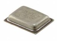
Through Hole Tube Active EAR99 Gate Drivers ICs Non-Inverting 8-DIP (0.300, 7.62mm) TC4420


Through Hole Tube Active EAR99 Gate Drivers ICs Non-Inverting 8-DIP (0.300, 7.62mm) TC4420
The TC4420CPA is a single-output MOSFET driver with a peak current of 6A. This article is going to introduce pinout, applications, features, and more details about TC4420CPA.

Pt. 1 Intro. TC4420-TC4429 High Power MOSFET Drivers
- Overview of TC4420CPA
- TC4420CPA Features
- TC4420CPA Pinout
- TC4420CPA Block Diagram
- TC4420CPA 3D Model
- Specifications
- TC4420CPA Electrical Characteristics
- TC4420CPA Technical Data
- TC4420CPA Applications
- TC4420CPA Package information
- TC4420CPA Warnings
- TC4420CPA Manufacturer
- Datasheet PDF
- Popularity by Region
- Parts with Similar Specs
Overview of TC4420CPA
The TC4420CPA is a single-output MOSFET driver with a peak current of 6A. The TC4420CPA is a non-inverting driver, while the TC4429 is an inverting driver (pin-compatible with the TC429). In comparison to bipolar drivers, these drivers are built-in CMOS for reduced power and more efficient operation. Both devices feature TTL /CMOS inputs that can be driven as high as VDD + 0.3V or as low as –5V without the device being agitated or damaged. External level-shifting circuitry and its accompanying expense and size are no longer required. The rail-to-rail output swing ensures improved drive voltage margin, especially during power-up/power-down sequencing.
The TC4420CPA is essentially latch-up proof, unlike other drivers. It can replace three or more discrete components, conserving PCB space, materials, and increasing system reliability.
TC4420CPA Features
Latch-Up Protected: Will Withstand >1.5AReverse Output Current
Logic Input Will Withstand Negative Swing Up To5V
ESD Protected: 4 kV
Matched Rise and Fall Times:- 25 ns (2500 pF load)
High Peak Output Current: 6A
Wide Input Supply Voltage Operating Range:- 4.5V to 18V
High Capacitive Load Drive Capability: 10,000 pF
Short Delay Time: 55 ns (Typ.)
CMOS/TTL Compatible Input
Low Supply Current With Logic ‘1’ Input:- 450 µA (Typ.)
Low Output Impedance: 2.5W
Output Voltage Swing to Within 25 mV of Ground or VDD
Space-Saving 8-Pin SOIC and 8-Pin 6x5 DFNPackages
TC4420CPA Pinout

TC4420CPA Pinout
TC4420CPA Block Diagram

TC4420CPA Block Diagram
TC4420CPA 3D Model

TC4420CPA Symbol

TC4420CPA Footprint

TC4420CPA 3D Model
Specifications
- TypeParameter
- Factory Lead Time6 Weeks
- Mount
In electronic components, the term "Mount" typically refers to the method or process of physically attaching or fixing a component onto a circuit board or other electronic device. This can involve soldering, adhesive bonding, or other techniques to secure the component in place. The mounting process is crucial for ensuring proper electrical connections and mechanical stability within the electronic system. Different components may have specific mounting requirements based on their size, shape, and function, and manufacturers provide guidelines for proper mounting procedures to ensure optimal performance and reliability of the electronic device.
Through Hole - Mounting Type
The "Mounting Type" in electronic components refers to the method used to attach or connect a component to a circuit board or other substrate, such as through-hole, surface-mount, or panel mount.
Through Hole - Package / Case
refers to the protective housing that encases an electronic component, providing mechanical support, electrical connections, and thermal management.
8-DIP (0.300, 7.62mm) - Number of Pins8
- Logic voltage-VIL, VIH0.8V 2.4V
- Driver ConfigurationLow-Side
- Turn Off Delay Time
It is the time from when Vgs drops below 90% of the gate drive voltage to when the drain current drops below 90% of the load current. It is the delay before current starts to transition in the load, and depends on Rg. Ciss.
25 ns - Usage LevelCommercial grade
- Operating Temperature
The operating temperature is the range of ambient temperature within which a power supply, or any other electrical equipment, operate in. This ranges from a minimum operating temperature, to a peak or maximum operating temperature, outside which, the power supply may fail.
0°C~150°C TJ - Packaging
Semiconductor package is a carrier / shell used to contain and cover one or more semiconductor components or integrated circuits. The material of the shell can be metal, plastic, glass or ceramic.
Tube - Published1997
- JESD-609 Code
The "JESD-609 Code" in electronic components refers to a standardized marking code that indicates the lead-free solder composition and finish of electronic components for compliance with environmental regulations.
e3 - Pbfree Code
The "Pbfree Code" parameter in electronic components refers to the code or marking used to indicate that the component is lead-free. Lead (Pb) is a toxic substance that has been widely used in electronic components for many years, but due to environmental concerns, there has been a shift towards lead-free alternatives. The Pbfree Code helps manufacturers and users easily identify components that do not contain lead, ensuring compliance with regulations and promoting environmentally friendly practices. It is important to pay attention to the Pbfree Code when selecting electronic components to ensure they meet the necessary requirements for lead-free applications.
yes - Part Status
Parts can have many statuses as they progress through the configuration, analysis, review, and approval stages.
Active - Moisture Sensitivity Level (MSL)
Moisture Sensitivity Level (MSL) is a standardized rating that indicates the susceptibility of electronic components, particularly semiconductors, to moisture-induced damage during storage and the soldering process, defining the allowable exposure time to ambient conditions before they require special handling or baking to prevent failures
1 (Unlimited) - Number of Terminations8
- ECCN Code
An ECCN (Export Control Classification Number) is an alphanumeric code used by the U.S. Bureau of Industry and Security to identify and categorize electronic components and other dual-use items that may require an export license based on their technical characteristics and potential for military use.
EAR99 - Terminal Finish
Terminal Finish refers to the surface treatment applied to the terminals or leads of electronic components to enhance their performance and longevity. It can improve solderability, corrosion resistance, and overall reliability of the connection in electronic assemblies. Common finishes include nickel, gold, and tin, each possessing distinct properties suitable for various applications. The choice of terminal finish can significantly impact the durability and effectiveness of electronic devices.
Matte Tin (Sn) - Max Power Dissipation
The maximum power that the MOSFET can dissipate continuously under the specified thermal conditions.
730mW - Voltage - Supply
Voltage - Supply refers to the range of voltage levels that an electronic component or circuit is designed to operate with. It indicates the minimum and maximum supply voltage that can be applied for the device to function properly. Providing supply voltages outside this range can lead to malfunction, damage, or reduced performance. This parameter is critical for ensuring compatibility between different components in a circuit.
4.5V~18V - Terminal Position
In electronic components, the term "Terminal Position" refers to the physical location of the connection points on the component where external electrical connections can be made. These connection points, known as terminals, are typically used to attach wires, leads, or other components to the main body of the electronic component. The terminal position is important for ensuring proper connectivity and functionality of the component within a circuit. It is often specified in technical datasheets or component specifications to help designers and engineers understand how to properly integrate the component into their circuit designs.
DUAL - Number of Functions1
- Terminal Pitch
The center distance from one pole to the next.
2.54mm - Base Part Number
The "Base Part Number" (BPN) in electronic components serves a similar purpose to the "Base Product Number." It refers to the primary identifier for a component that captures the essential characteristics shared by a group of similar components. The BPN provides a fundamental way to reference a family or series of components without specifying all the variations and specific details.
TC4420 - Pin Count
a count of all of the component leads (or pins)
8 - Number of Outputs1
- Output Voltage
Output voltage is a crucial parameter in electronic components that refers to the voltage level produced by the component as a result of its operation. It represents the electrical potential difference between the output terminal of the component and a reference point, typically ground. The output voltage is a key factor in determining the performance and functionality of the component, as it dictates the level of voltage that will be delivered to the connected circuit or load. It is often specified in datasheets and technical specifications to ensure compatibility and proper functioning within a given system.
18V - Max Output Current
The maximum current that can be supplied to the load.
6A - Nominal Supply Current
Nominal current is the same as the rated current. It is the current drawn by the motor while delivering rated mechanical output at its shaft.
3mA - Power Dissipation
the process by which an electronic or electrical device produces heat (energy loss or waste) as an undesirable derivative of its primary action.
730mW - Output Current
The rated output current is the maximum load current that a power supply can provide at a specified ambient temperature. A power supply can never provide more current that it's rated output current unless there is a fault, such as short circuit at the load.
6A - Max Supply Current
Max Supply Current refers to the maximum amount of electrical current that a component can draw from its power supply under normal operating conditions. It is a critical parameter that ensures the component operates reliably without exceeding its thermal limits or damaging internal circuitry. Exceeding this current can lead to overheating, performance degradation, or failure of the component. Understanding this parameter is essential for designing circuits that provide adequate power while avoiding overload situations.
1.5mA - Propagation Delay
the flight time of packets over the transmission link and is limited by the speed of light.
75 ns - Input Type
Input type in electronic components refers to the classification of the signal or data that a component can accept for processing or conversion. It indicates whether the input is analog, digital, or a specific format such as TTL or CMOS. Understanding input type is crucial for ensuring compatibility between different electronic devices and circuits, as it determines how signals are interpreted and interacted with.
Non-Inverting - Turn On Delay Time
Turn-on delay, td(on), is the time taken to charge the input capacitance of the device before drain current conduction can start.
25 ns - Max Output Voltage
The maximum output voltage refers to the dynamic area beyond which the output is saturated in the positive or negative direction, and is limited according to the load resistance value.
-25mV - Rise Time
In electronics, when describing a voltage or current step function, rise time is the time taken by a signal to change from a specified low value to a specified high value.
60ns - Fall Time (Typ)
Fall Time (Typ) is a parameter used to describe the time it takes for a signal to transition from a high level to a low level in an electronic component, such as a transistor or an integrated circuit. It is typically measured in nanoseconds or microseconds and is an important characteristic that affects the performance of the component in digital circuits. A shorter fall time indicates faster switching speeds and can result in improved overall circuit performance, such as reduced power consumption and increased data transmission rates. Designers often consider the fall time specification when selecting components for their circuits to ensure proper functionality and efficiency.
35 ns - Rise / Fall Time (Typ)
The parameter "Rise / Fall Time (Typ)" in electronic components refers to the time it takes for a signal to transition from a specified low level to a specified high level (rise time) or from a high level to a low level (fall time). It is typically measured in nanoseconds or picoseconds and is an important characteristic in determining the speed and performance of a component, such as a transistor or integrated circuit. A shorter rise/fall time indicates faster signal switching and can impact the overall speed and efficiency of a circuit. Designers often consider this parameter when selecting components for high-speed applications to ensure proper signal integrity and timing.
25ns 25ns - Interface IC Type
The parameter "Interface IC Type" in electronic components refers to the type of integrated circuit (IC) that is used to facilitate communication between different electronic devices or subsystems. This IC is responsible for managing the exchange of data and control signals between the devices, ensuring proper communication and coordination. The specific type of interface IC used can vary depending on the requirements of the system, such as serial communication (e.g., UART, SPI, I2C), parallel communication, or specialized interfaces like USB or Ethernet. Choosing the appropriate interface IC type is crucial for ensuring compatibility, reliability, and efficiency in electronic systems.
BUFFER OR INVERTER BASED MOSFET DRIVER - Channel Type
In electronic components, the parameter "Channel Type" refers to the type of channel through which electrical signals or current flow within the component. This parameter is commonly associated with field-effect transistors (FETs) and other semiconductor devices. The channel type can be categorized as either N-channel or P-channel, depending on the polarity of the majority charge carriers (electrons or holes) that carry the current within the channel. N-channel devices have an electron-conducting channel, while P-channel devices have a hole-conducting channel. Understanding the channel type is crucial for proper circuit design and component selection to ensure compatibility and optimal performance.
Single - Input Bias Current
Input Bias Current refers to the small amount of current that flows into the input terminals of an electronic component, such as an operational amplifier. It is primarily caused by the input impedance of the device and the characteristics of the transistors within it. This current is crucial in determining the accuracy of the analog signal processing, as it can affect the level of voltage offset and signal integrity in the application. In many precise applications, minimizing input bias current is essential to achieve optimal performance.
10μA - Output Peak Current Limit-Nom
Output Peak Current Limit-Nom is a parameter in electronic components that specifies the maximum current that can be delivered by the output under normal operating conditions. This limit is typically set to protect the component from damage due to excessive current flow. It ensures that the component operates within its safe operating limits and prevents overheating or other potential issues. Designers and engineers use this parameter to ensure proper functioning and reliability of the electronic system in which the component is used.
6A - Gate Type
In electronic components, the term "Gate Type" typically refers to the type of logic gate used in digital circuits. A logic gate is a fundamental building block of digital circuits that performs a specific logical operation based on the input signals it receives. Common types of logic gates include AND, OR, NOT, NAND, NOR, XOR, and XNOR gates.The Gate Type parameter specifies the specific logic function that the gate performs, such as AND, OR, or NOT. Different gate types have different truth tables that define their behavior based on the input signals. By selecting the appropriate gate type for a given application, designers can implement various logical functions and operations in digital circuits.Understanding the gate type is essential for designing and analyzing digital circuits, as it determines how the circuit processes and manipulates binary data. Choosing the right gate type is crucial for ensuring the correct functionality and performance of the digital system being designed.
N-Channel, P-Channel MOSFET - Current - Peak Output (Source, Sink)
The parameter "Current - Peak Output (Source, Sink)" in electronic components refers to the maximum amount of current that the component can either supply (source) or sink (absorb) under peak conditions. This parameter is important for understanding the capability of the component to handle sudden surges or spikes in current without being damaged. The peak output current is typically specified in datasheets and is crucial for designing circuits that require high current handling capabilities. It is essential to consider this parameter to ensure the component operates within its safe operating limits and to prevent potential damage or malfunction.
6A 6A - High Side Driver
A High Side Driver is an electronic component used in power management applications to control the switching of high-side power devices such as MOSFETs or IGBTs. It is designed to drive the gate or base of the power device to turn it on or off, allowing current to flow through the load or cutting off the current flow. High Side Drivers are commonly used in automotive, industrial, and consumer electronics to control various loads such as motors, solenoids, and heaters. They provide isolation between the control circuitry and the high-side power device, ensuring safe and reliable operation of the system.
YES - Length9.46mm
- Height3.3mm
- Width6.35mm
- REACH SVHC
The parameter "REACH SVHC" in electronic components refers to the compliance with the Registration, Evaluation, Authorization, and Restriction of Chemicals (REACH) regulation regarding Substances of Very High Concern (SVHC). SVHCs are substances that may have serious effects on human health or the environment, and their use is regulated under REACH to ensure their safe handling and minimize their impact.Manufacturers of electronic components need to declare if their products contain any SVHCs above a certain threshold concentration and provide information on the safe use of these substances. This information allows customers to make informed decisions about the potential risks associated with using the components and take appropriate measures to mitigate any hazards.Ensuring compliance with REACH SVHC requirements is essential for electronics manufacturers to meet regulatory standards, protect human health and the environment, and maintain transparency in their supply chain. It also demonstrates a commitment to sustainability and responsible manufacturing practices in the electronics industry.
No SVHC - Radiation Hardening
Radiation hardening is the process of making electronic components and circuits resistant to damage or malfunction caused by high levels of ionizing radiation, especially for environments in outer space (especially beyond the low Earth orbit), around nuclear reactors and particle accelerators, or during nuclear accidents or nuclear warfare.
No - RoHS Status
RoHS means “Restriction of Certain Hazardous Substances” in the “Hazardous Substances Directive” in electrical and electronic equipment.
ROHS3 Compliant - Lead Free
Lead Free is a term used to describe electronic components that do not contain lead as part of their composition. Lead is a toxic material that can have harmful effects on human health and the environment, so the electronics industry has been moving towards lead-free components to reduce these risks. Lead-free components are typically made using alternative materials such as silver, copper, and tin. Manufacturers must comply with regulations such as the Restriction of Hazardous Substances (RoHS) directive to ensure that their products are lead-free and environmentally friendly.
Lead Free
TC4420CPA Electrical Characteristics
| Electrical Specifications: Unless otherwise noted, TA = +25°C with 4.5V VDD 18V | ||||||
| Parameters | Sym | Min | Typ | Max | Units | Conditions |
| Input | ||||||
| Logic ‘1’, High Input Voltage | VIH | 2.4 | 1.8 | _ | V | |
| Logic ‘0’, Low Input Voltage | VIL | _ | 1.3 | 0.8 | V | |
| Input Voltage Range | VIN | –5 | _ | VDD+0.3 | V | |
| Input Current | IIN | –10 | _ | 10 | µA | 0VVINVDD |
| Output | ||||||
| High Output Voltage | VOH | VDD – 0.025 | _ | _ | V | DC TEST |
| Low Output Voltage | VOL | _ | _ | 0.025 | V | DC TEST |
| Output Resistance, High | ROH | _ | 2.1 | 2.8 | | IOUT = 10 mA, VDD = 18V |
| Output Resistance, Low | ROL | _ | 1.5 | 2.5 | | IOUT = 10 mA, VDD = 18V |
| Peak Output Current | IPK | _ | 6 | _ | A | VDD = 18V |
| Latch-Up Protection Withstand Reverse Current | IREV | _ | > 1.5 | _ | A | Duty cycle2%, t 300 µsec |
| Switching Time (Note 1) | ||||||
| Rise Time | tR | _ | 25 | 35 | ns | Figure 4-1, CL = 2,500 pF |
| Fall Time | tF | _ | 25 | 35 | ns | Figure 4-1, CL = 2,500 pF |
| Delay Time | tD1 | _ | 55 | 75 | ns | Figure 4-1 |
| Power Supply | ||||||
| Power Supply Current | IS | _ | 0.45 55 | 1.5 150 | mA µA | VIN = 3V VIN = 0V |
| Operating Input Voltage | VDD | 4.5 | _ | 18 | V | |
TC4420CPA Technical Data
| Technical | |
| Fall Time | 35 ns |
| Input Bias Current | 10 µA |
| Max Operating Temperature | 70 °C |
| Max Output Current | 6 A |
| Max Output Voltage | -25 mV |
| Max Power Dissipation | 730 mW |
| Max Supply Current | 1.5 mA |
| Max Supply Voltage | 18 V |
| Min Operating Temperature | 0 °C |
| Min Supply Voltage | 4.5 V |
| Nominal Supply Current | 3 mA |
| Number of Channels | 1 |
| Number of Drivers | 1 |
| Number of Outputs | 1 |
| Output Current | 6 A |
| Output Voltage | 18 V |
| Packaging | Bulk |
| Power Dissipation | 730 mW |
| Propagation Delay | 75 ns |
| Rise Time | 60 ns |
| Schedule B | 8542390000, 8542390000|8542390000, 8542390000|8542390000|8542390000, 8542390000|8542390000|8542390000|8542390000 |
| Turn-Off Delay Time | 25 ns |
| Turn-On Delay Time | 25 ns |
TC4420CPA Applications
• Switch-Mode Power Supplies
• Motor Controls
• Pulse Transformer Driver
• Class D Switching Amplifiers
TC4420CPA Package information

TC4420CPA Package information
TC4420CPA Warnings
ESD sensitive device, take proper precaution while handling the device. Market demand for this product has caused an extension in lead times. Delivery dates may fluctuate. Product exempt from discounts.
TC4420CPA Manufacturer
Microchip Technology Inc. is a leading provider of microcontroller and analog semiconductors, delivering low-risk product development, reduced overall system cost, and faster time to market to thousands of customers across the world. Microchip, based in Chandler, Arizona, provides excellent technical support as well as consistent delivery and quality.
Datasheet PDF
- Datasheets :
- PCN Packaging :
- ConflictMineralStatement :
Popularity by Region
Parts with Similar Specs
- ImagePart NumberManufacturerPackage / CaseNumber of PinsMax Output CurrentOutput CurrentRise TimeMax Power DissipationPower DissipationNumber of TerminationsView Compare
![TC4420CPA]()
TC4420CPA
8-DIP (0.300, 7.62mm)
8
6 A
6 A
60 ns
730 mW
730 mW
8
![TC428CPA]()
8-DIP (0.300, 7.62mm)
8
6 A
6 A
60 ns
730 mW
730 mW
8
![TC4429CPA]()
8-DIP (0.300, 7.62mm)
8
1.5 A
1.5 A
30 ns
730 mW
730 mW
8
![MAX4420CPA]()
8-DIP (0.300, 7.62mm)
8
6 A
6 A
25 ns
727 mW
-
8
![TC4427CPA]()
8-DIP (0.300, 7.62mm)
8
1.5 A
1.5 A
30 ns
730 mW
730 mW
8

How many pins of TC4420CPA ?
8 pins.
What’s the operating temperature of TC4420CPA ?
0°C~150°C TJ.
What’s the Voltage - Supply of TC4420CPA ?
4.5V~18V.
What’s the output voltage of TC4420CPA ?
18V.
What’s the output current of TC4420CPA ?
6A.
 SPH0641LM4H-1 Digital Microphone: Circuit, Pinout, and Datasheet
23 February 20227162
 CR2016 vs. CR2032: Specifications, Applications, Differences
04 November 202190667
 PN2222 Vs. 2N2222: They Are Equivalents In Most Cases
01 March 202210866
 MPS2222A Transistor:MPS2222A vs. 2N2222,MPS2222A Datasheet
14 March 20227706
![SS54 DIODE SCHOTTKY 5A 40V SMA[Video+FAQ]](https://res.utmel.com/Images/Article/797cab1e-638e-41cf-95d3-366d7c01d783.png) SS54 DIODE SCHOTTKY 5A 40V SMA[Video+FAQ]
SS54 DIODE SCHOTTKY 5A 40V SMA[Video+FAQ]23 April 202210174
- How to select and source STMicroelectronics UC3845BN
16 August 2025191
 CC2541 MCU: Pinout, Circuit, Application
14 August 20214355
 LTST-C191KRKT SMD LED: Circuit, Pinout, and Datasheet
08 March 20222345
 India's Bold Leap Towards Semiconductor Supremacy
15 September 20233822
 What is a Ceramic Filter?
10 April 20214633
 Introduction to Distribution Transformer
24 February 20219255
 Diode Basis: Symbol, Types and Applications
09 January 202614391
 What is Tantalum Capacitor: Structure, Failure and Application Guide
14 April 202220577
 Utmel, China's Leading Overseas Component Distributor, at PCIM Europe 2023
10 November 20237625
 Understanding UARTs: The Basics and Benefits of Serial Communication
06 March 20233048
 How Do We Seize Investment Opportunities on the Eve of the Ultimate Human Energy Final?
12 July 20222219
Microchip Technology
In Stock: 2
United States
China
Canada
Japan
Russia
Germany
United Kingdom
Singapore
Italy
Hong Kong(China)
Taiwan(China)
France
Korea
Mexico
Netherlands
Malaysia
Austria
Spain
Switzerland
Poland
Thailand
Vietnam
India
United Arab Emirates
Afghanistan
Åland Islands
Albania
Algeria
American Samoa
Andorra
Angola
Anguilla
Antigua & Barbuda
Argentina
Armenia
Aruba
Australia
Azerbaijan
Bahamas
Bahrain
Bangladesh
Barbados
Belarus
Belgium
Belize
Benin
Bermuda
Bhutan
Bolivia
Bonaire, Sint Eustatius and Saba
Bosnia & Herzegovina
Botswana
Brazil
British Indian Ocean Territory
British Virgin Islands
Brunei
Bulgaria
Burkina Faso
Burundi
Cabo Verde
Cambodia
Cameroon
Cayman Islands
Central African Republic
Chad
Chile
Christmas Island
Cocos (Keeling) Islands
Colombia
Comoros
Congo
Congo (DRC)
Cook Islands
Costa Rica
Côte d’Ivoire
Croatia
Cuba
Curaçao
Cyprus
Czechia
Denmark
Djibouti
Dominica
Dominican Republic
Ecuador
Egypt
El Salvador
Equatorial Guinea
Eritrea
Estonia
Eswatini
Ethiopia
Falkland Islands
Faroe Islands
Fiji
Finland
French Guiana
French Polynesia
Gabon
Gambia
Georgia
Ghana
Gibraltar
Greece
Greenland
Grenada
Guadeloupe
Guam
Guatemala
Guernsey
Guinea
Guinea-Bissau
Guyana
Haiti
Honduras
Hungary
Iceland
Indonesia
Iran
Iraq
Ireland
Isle of Man
Israel
Jamaica
Jersey
Jordan
Kazakhstan
Kenya
Kiribati
Kosovo
Kuwait
Kyrgyzstan
Laos
Latvia
Lebanon
Lesotho
Liberia
Libya
Liechtenstein
Lithuania
Luxembourg
Macao(China)
Madagascar
Malawi
Maldives
Mali
Malta
Marshall Islands
Martinique
Mauritania
Mauritius
Mayotte
Micronesia
Moldova
Monaco
Mongolia
Montenegro
Montserrat
Morocco
Mozambique
Myanmar
Namibia
Nauru
Nepal
New Caledonia
New Zealand
Nicaragua
Niger
Nigeria
Niue
Norfolk Island
North Korea
North Macedonia
Northern Mariana Islands
Norway
Oman
Pakistan
Palau
Palestinian Authority
Panama
Papua New Guinea
Paraguay
Peru
Philippines
Pitcairn Islands
Portugal
Puerto Rico
Qatar
Réunion
Romania
Rwanda
Samoa
San Marino
São Tomé & Príncipe
Saudi Arabia
Senegal
Serbia
Seychelles
Sierra Leone
Sint Maarten
Slovakia
Slovenia
Solomon Islands
Somalia
South Africa
South Sudan
Sri Lanka
St Helena, Ascension, Tristan da Cunha
St. Barthélemy
St. Kitts & Nevis
St. Lucia
St. Martin
St. Pierre & Miquelon
St. Vincent & Grenadines
Sudan
Suriname
Svalbard & Jan Mayen
Sweden
Syria
Tajikistan
Tanzania
Timor-Leste
Togo
Tokelau
Tonga
Trinidad & Tobago
Tunisia
Turkey
Turkmenistan
Turks & Caicos Islands
Tuvalu
U.S. Outlying Islands
U.S. Virgin Islands
Uganda
Ukraine
Uruguay
Uzbekistan
Vanuatu
Vatican City
Venezuela
Wallis & Futuna
Yemen
Zambia
Zimbabwe
![TC4426EOA713]() TC4426EOA713
TC4426EOA713Microchip Technology
![TC4427EOA713]() TC4427EOA713
TC4427EOA713Microchip Technology
![TC4426AEOA713]() TC4426AEOA713
TC4426AEOA713Microchip Technology
![TC4422AVOA]() TC4422AVOA
TC4422AVOAMicrochip Technology
![MCP1402T-E/OT]() MCP1402T-E/OT
MCP1402T-E/OTMicrochip Technology
![MCP1416T-E/OT]() MCP1416T-E/OT
MCP1416T-E/OTMicrochip Technology
![MIC4427YMM]() MIC4427YMM
MIC4427YMMMicrochip Technology
![TC4426ACOA]() TC4426ACOA
TC4426ACOAMicrochip Technology
![TC4426EOA]() TC4426EOA
TC4426EOAMicrochip Technology
![TC4427ACOA713]() TC4427ACOA713
TC4427ACOA713Microchip Technology


