
 Product
 Brand
Brand Articles
 Tools
Tools
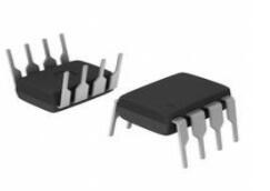
XRP7675 Step-Down Regulator: Pinout, Features and Datasheet

4.5V DC DC Voltage Regulator SWITCHING REGULATOR 1 Outputs 340kHz Tape & Reel (TR) 8-SOIC (0.154, 3.90mm Width) Exposed Pad
Unit Price: $0.530432
Ext Price: $0.53


4.5V DC DC Voltage Regulator SWITCHING REGULATOR 1 Outputs 340kHz Tape & Reel (TR) 8-SOIC (0.154, 3.90mm Width) Exposed Pad
The XRP7675 is a 3A capable synchronous current-mode PWM step down (buck) voltage regulator with improved light current load efficiency. Furthermore, Huge range of Semiconductors, Capacitors, Resistors and IcS in stock. Welcome RFQ.
XRP7675 Pinout
The following figure is the diagram of XRP7675 Pinout.

Pinout
XRP7675 CAD Model
The followings are XRP7675 Footprint and 3D Model.

Footprint

3D Model
XRP7675 Description
The XRP7675 is a 3A capable synchronous current-mode PWM step down (buck) voltage regulator with improved light current load efficiency. A wide 4.5V to 18V input voltage range allows for single supply operations from industry standard 5V and 12V power rails. With a 340kHz constant operating frequency and integrated high and low-side 100mΩ/100mΩ MOSFETs, the XRP7675 reduces the overall component count and solution footprint. Current-mode control provides fast transient response and cycle-by-cycle OCP. An adjustable soft-start prevents inrush current at turn-on, and in shutdown mode the supply current drops to 0.1μA. At light current loads, the XRP7675 operates in Discontinuous Conduction Mode (DCM) and is complemented by a pulse frequency modulation mode (PFM) to provide excellent conversion efficiency. Built-in output over-voltage (open load), over temperature, cycle-by-cycle over-current, under-voltage lockout (UVLO) and hiccup mode short-circuit protection insures safe operation under abnormal operating conditions. The XRP7675 is offered in a RoHS compliant, “green" / halogen free 8-pin Exposed Pad SOIC package.
This article will introduce XRP7675 systematically from its features, pinout to its specifications, applications, also including XRP7675 datasheet and so much more.
XRP7675 Features
● 3A Continuous Output Current
● 4.5V to 18V Wide Input Voltage
◆ 0.925V to 16V Adjustable Output Voltage
◆ ±2% Output Voltage Accuracy
● PWM Current-Mode Control
◆ 340kHz Constant Operations
◆ Up to 95% Efficiency
● Light-Load Efficiency
◆ Discontinuous Conduction Mode (DCM)
◆ Pulse Frequency Modulation Mode (PFM)
● Programmable Soft-Start and Enable Function
● Built-in Thermal, Over-Current, UVLO, Output Over-Voltage and hiccup mode short-circuit protection
● RoHS Compliant, "Green"/Halogen Free 8-Pin Exposed Pad SOIC Package
Specifications
- TypeParameter
- Factory Lead Time16 Weeks
- Package / Case
refers to the protective housing that encases an electronic component, providing mechanical support, electrical connections, and thermal management.
8-SOIC (0.154, 3.90mm Width) Exposed Pad - Mounting Type
The "Mounting Type" in electronic components refers to the method used to attach or connect a component to a circuit board or other substrate, such as through-hole, surface-mount, or panel mount.
Surface Mount - Packaging
Semiconductor package is a carrier / shell used to contain and cover one or more semiconductor components or integrated circuits. The material of the shell can be metal, plastic, glass or ceramic.
Tape & Reel (TR) - Operating Temperature
The operating temperature is the range of ambient temperature within which a power supply, or any other electrical equipment, operate in. This ranges from a minimum operating temperature, to a peak or maximum operating temperature, outside which, the power supply may fail.
-40°C~85°C TA - JESD-609 Code
The "JESD-609 Code" in electronic components refers to a standardized marking code that indicates the lead-free solder composition and finish of electronic components for compliance with environmental regulations.
e3 - Part Status
Parts can have many statuses as they progress through the configuration, analysis, review, and approval stages.
Active - Moisture Sensitivity Level (MSL)
Moisture Sensitivity Level (MSL) is a standardized rating that indicates the susceptibility of electronic components, particularly semiconductors, to moisture-induced damage during storage and the soldering process, defining the allowable exposure time to ambient conditions before they require special handling or baking to prevent failures
1 (Unlimited) - ECCN Code
An ECCN (Export Control Classification Number) is an alphanumeric code used by the U.S. Bureau of Industry and Security to identify and categorize electronic components and other dual-use items that may require an export license based on their technical characteristics and potential for military use.
EAR99 - Terminal Finish
Terminal Finish refers to the surface treatment applied to the terminals or leads of electronic components to enhance their performance and longevity. It can improve solderability, corrosion resistance, and overall reliability of the connection in electronic assemblies. Common finishes include nickel, gold, and tin, each possessing distinct properties suitable for various applications. The choice of terminal finish can significantly impact the durability and effectiveness of electronic devices.
MATTE TIN - Peak Reflow Temperature (Cel)
Peak Reflow Temperature (Cel) is a parameter that specifies the maximum temperature at which an electronic component can be exposed during the reflow soldering process. Reflow soldering is a common method used to attach electronic components to a circuit board. The Peak Reflow Temperature is crucial because it ensures that the component is not damaged or degraded during the soldering process. Exceeding the specified Peak Reflow Temperature can lead to issues such as component failure, reduced performance, or even permanent damage to the component. It is important for manufacturers and assemblers to adhere to the recommended Peak Reflow Temperature to ensure the reliability and functionality of the electronic components.
260 - Time@Peak Reflow Temperature-Max (s)
Time@Peak Reflow Temperature-Max (s) refers to the maximum duration that an electronic component can be exposed to the peak reflow temperature during the soldering process, which is crucial for ensuring reliable solder joint formation without damaging the component.
40 - Function
The parameter "Function" in electronic components refers to the specific role or purpose that the component serves within an electronic circuit. It defines how the component interacts with other elements, influences the flow of electrical signals, and contributes to the overall behavior of the system. Functions can include amplification, signal processing, switching, filtering, and energy storage, among others. Understanding the function of each component is essential for designing effective and efficient electronic systems.
Step-Down - Number of Outputs1
- Voltage - Input (Max)
Voltage - Input (Max) is a parameter in electronic components that specifies the maximum voltage that can be safely applied to the input of the component without causing damage. This parameter is crucial for ensuring the proper functioning and longevity of the component. Exceeding the maximum input voltage can lead to electrical overstress, which may result in permanent damage or failure of the component. It is important to carefully adhere to the specified maximum input voltage to prevent any potential issues and maintain the reliability of the electronic system.
18V - Output Type
The "Output Type" parameter in electronic components refers to the type of signal or data that is produced by the component as an output. This parameter specifies the nature of the output signal, such as analog or digital, and can also include details about the voltage levels, current levels, frequency, and other characteristics of the output signal. Understanding the output type of a component is crucial for ensuring compatibility with other components in a circuit or system, as well as for determining how the output signal can be utilized or processed further. In summary, the output type parameter provides essential information about the nature of the signal that is generated by the electronic component as its output.
Adjustable - Voltage - Input (Min)
Voltage - Input (Min) refers to the minimum voltage level that an electronic component requires to operate correctly. It indicates the lowest voltage that can be applied to the component while still allowing it to function as intended. If the input voltage falls below this specified minimum, the component may not perform properly or may fail to operate altogether. This parameter is critical for ensuring reliable operation and longevity of the device in electronic circuits.
4.5V - Analog IC - Other Type
Analog IC - Other Type is a parameter used to categorize electronic components that are integrated circuits (ICs) designed for analog signal processing but do not fall into more specific subcategories such as amplifiers, comparators, or voltage regulators. These ICs may include specialized analog functions such as analog-to-digital converters (ADCs), digital-to-analog converters (DACs), voltage references, or signal conditioning circuits. They are typically used in various applications where precise analog signal processing is required, such as in audio equipment, instrumentation, communication systems, and industrial control systems. Manufacturers provide detailed specifications for these components to help engineers select the most suitable IC for their specific design requirements.
SWITCHING REGULATOR - Output Configuration
Output Configuration in electronic components refers to the arrangement or setup of the output pins or terminals of a device. It defines how the output signals are structured and how they interact with external circuits or devices. The output configuration can determine the functionality and compatibility of the component in a circuit design. Common types of output configurations include single-ended, differential, open-drain, and push-pull configurations, each serving different purposes and applications in electronic systems. Understanding the output configuration of a component is crucial for proper integration and operation within a circuit.
Positive - Voltage - Output (Min/Fixed)
Voltage - Output (Min/Fixed) refers to the minimum fixed output voltage level that an electronic component, such as a voltage regulator or power supply, is designed to provide under specified load conditions. This parameter ensures that the device consistently delivers a reliable voltage that meets the requirements of the connected circuits or components. It is critical for applications where stable and predictable voltage is necessary for proper operation.
0.925V - Topology
In the context of electronic components, "topology" refers to the arrangement or configuration of the components within a circuit or system. It defines how the components are connected to each other and how signals flow between them. The choice of topology can significantly impact the performance, efficiency, and functionality of the electronic system. Common topologies include series, parallel, star, mesh, and hybrid configurations, each with its own advantages and limitations. Designers carefully select the appropriate topology based on the specific requirements of the circuit to achieve the desired performance and functionality.
Buck - Frequency - Switching
"Frequency - Switching" in electronic components refers to the rate at which a device, such as a transistor or switching regulator, turns on and off during operation. This parameter is crucial in determining the efficiency and performance of power converters, oscillators, and other circuits that rely on rapid switching. Higher switching frequencies typically allow for smaller component sizes but may require more advanced design considerations to manage heat and electromagnetic interference.
340kHz - Synchronous Rectifier
Synchronous rectification is a technique for improving the efficiency of rectification by replacing diodes with actively controlled switches, usually power MOSFETs or power bipolar junction transistors (BJT).
Yes - RoHS Status
RoHS means “Restriction of Certain Hazardous Substances” in the “Hazardous Substances Directive” in electrical and electronic equipment.
RoHS Compliant
XRP7675 Functional Block Diagram
The following is the Block Diagram of XRP7675.

XRP7675 Block Diagram
XRP7675 Applications
● Distributed Power Architecture
● Portable Equipment
● Point of Load Converter
● Audio-Video Equipment
XRP7675 Typical Application Diagram
The following diagram shows the XRP7675 Application Diagram.

XRP7675 Application Diagram
XRP7675 Package
The following diagrams show the XRP7675 Package.

View A

View B

View C
XRP7675 Manufacturer
MaxLinear delivers high-performance broadband and networking semiconductors based on its highly integrated radio frequency analog technology, high-performance optical networking technology and its pioneering MoCA and Direct Broadcast Satellite ODU single-wire technology.
Trend Analysis
Datasheet PDF
- PCN Obsolescence/ EOL :
- Datasheets :
- PCN Part Status Change :
How many pins of XRP7675?
8 Pins.
What’s the operating temperature of XRP7675?
-40°C~85°C TA.
What is the essential property of the XRP7675?
The XRP7675 is a 3A capable synchronous current-mode PWM step down (buck) voltage regulator with improved light current load efficiency.
Can XRP7675 use external components to compensate regulators?
XRP7675 utilizes current-mode control. This allows using a minimum of external components to compensate the regulator.
 2N5458 JFET: Alternatives, Datasheet, Pinout
07 October 20217952
 Microchip PIC18LF67K40IMR Technical Overview
29 February 2024115
 A6210 LED Driver: Datasheet, Pinout, Alternatives
15 September 2021838
 STM32F051C6T7 Microcontroller: Datasheet, Pinout, Block Diagram
13 September 20212162
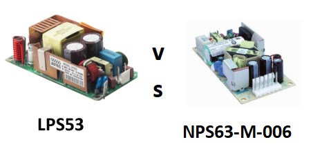 LPS53 vs NPS63-M-006
11 January 2022364
 TL071 OP-AMP: Where & How to Use TL071?
16 November 202118890
 BR2032 Battery: Panasonic BR2032, BR2032 vs. CR2032, Datasheet
23 April 202210690
 ATmega328P Series: 8-bit AVR Microcontroller Design Guide
15 January 2026585
 Exploring SPI Communication for Faster Data Transfer
20 June 2025747
 Comparing Popular Jumper Wires for Electronics Projects
10 July 20251420
 Detailed Analysis of Analog IC
22 November 20213421
 RF Mixer: Types, Applications, and Practical Guide
12 May 20254847
 Introduction to Photonic Integrated Circuits and PIC Technology
22 October 202514442
 Everything You Need to Know About Fuse Resistors
30 July 20252175
 Degson Authorized Distributor | UTMEL Electronics
21 November 20233709
 RTD Sensors: Working Principle, Features and Applications
22 May 202512759
MaxLinear, Inc.
In Stock: 25
Minimum: 1 Multiples: 1
Qty
Unit Price
Ext Price
1
$0.530432
$0.53
10
$0.500408
$5.00
100
$0.472083
$47.21
500
$0.445361
$222.68
1000
$0.420152
$420.15
Not the price you want? Send RFQ Now and we'll contact you ASAP.
Inquire for More Quantity
![XR76116ELTR-F]() XR76116ELTR-F
XR76116ELTR-FMaxLinear
![SP4446EK-L/TR]() SP4446EK-L/TR
SP4446EK-L/TRMaxLinear
![XR77103ELB]() XR77103ELB
XR77103ELBMaxLinear
![SP6669DEK-L]() SP6669DEK-L
SP6669DEK-LMaxLinear
![XRP76591STR-F]() XRP76591STR-F
XRP76591STR-FMaxLinear
![XRP6657IHB-F]() XRP6657IHB-F
XRP6657IHB-FMaxLinear
![XR76116BELTR-F]() XR76116BELTR-F
XR76116BELTR-FMaxLinear
![SP6832EK]() SP6832EK
SP6832EKMaxLinear
![XR76116BEL-F]() XR76116BEL-F
XR76116BEL-FMaxLinear
![SP6669AEK-L/TRR3]() SP6669AEK-L/TRR3
SP6669AEK-L/TRR3MaxLinear, Inc.

