

 Product
 Brand
Brand Articles
 Tools
Tools
What Is an In-Memory Computing Chip? Architecture, Silicon Technologies, and Real-World Hardware
Quick answer
An in-memory computing chip reduces data movement by performing selected operations inside a memory array or very close to it. The term covers several architectures rather than one universal chip type. Analog compute-in-memory (CIM) can perform matrix operations through physical electrical behavior, digital CIM adds logic to or around memory arrays, and processing-in-memory (PIM) places programmable processing resources near high-capacity memory. These approaches can improve latency or energy efficiency for suitable data-intensive workloads, but the result depends on precision, memory capacity, peripheral circuits, software support, and the scope of the benchmark.
Why data movement matters
Conventional processors repeatedly move operands and intermediate results between compute units, caches, and external memory. For workloads with low arithmetic intensity, the time and energy spent transferring data can become more important than the arithmetic itself. Large embedding lookups, recommendation systems, graph analytics, database scans, and some neural-network layers are common examples. However, a workload should not be described as universally "memory-bound" without measuring the actual model, batch size, precision, memory hierarchy, and processor utilization.
In-memory computing changes where selected operations happen. Instead of fetching every weight or database item into a distant processor, the system performs part of the work where the data is stored. The potential benefit is therefore not simply "faster memory." It is a reduction in transfers across expensive interfaces. The tradeoff is that memory arrays, peripheral circuits, compilers, and algorithms must be designed together.
CIM, PIM, and near-memory terminology
Terminology varies across academic papers and vendors. The following definitions are useful for engineering comparison, but product documentation may use the labels differently.
| Term | Where computation occurs | Practical interpretation |
|---|---|---|
| Compute-in-memory (CIM or IMC) | Within the memory array or its tightly coupled sensing and logic circuitry | Often used for parallel multiply-accumulate, Boolean, search, or reduction operations. It can be analog, mixed-signal, or digital. |
| Processing-in-memory (PIM) | In or alongside a memory device, stack, module, or bank | Usually includes programmable or fixed-function digital processing resources near higher-capacity memory. |
| Near-memory computing | On a logic die, chiplet, interposer, or accelerator close to memory | Reduces distance and interface traffic without requiring arithmetic inside the memory cells. |
The boundaries are not absolute. A DRAM module containing simple processors may be called PIM, while an SRAM macro that performs digital dot products may be called CIM. When comparing two platforms, inspect the data path and supported operations instead of relying on the marketing label.
How analog and digital in-memory computing work
Analog and mixed-signal CIM
In an idealized crossbar, each programmable cell represents a conductance related to a weight. Inputs are encoded as voltages, pulses, or time-domain signals. Currents accumulate along columns, allowing many multiply-accumulate contributions to be evaluated in parallel. In simplified form, an output can be written as yj = sum(wijxi). Real designs also need signed-weight encoding, multibit inputs and weights, reference paths, calibration, and conversion between digital and analog domains.
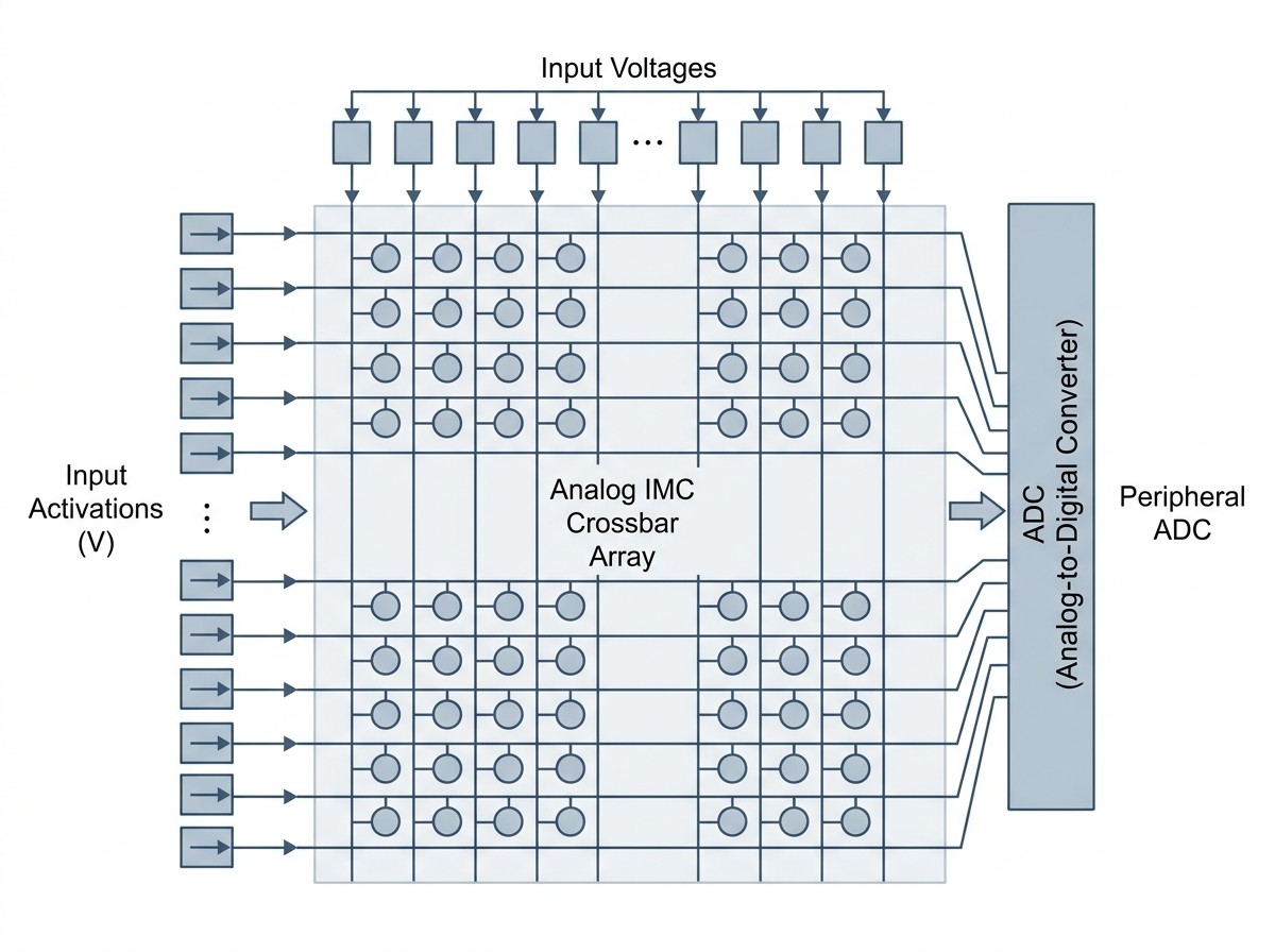
Analog CIM is attractive because the array uses device physics to perform many operations concurrently. The same physics creates engineering constraints: device-to-device variation, conductance drift, line resistance, noise, limited effective precision, programming overhead, and the energy and area of data converters. ADCs, DACs, drivers, and accumulation logic can dominate a design in some operating points, so array-only efficiency does not describe system efficiency.
Digital CIM
Digital CIM performs logic or arithmetic using digital states in or next to a memory macro. SRAM-based designs may activate modified bit cells and local logic to execute Boolean operations, population counts, bit-serial multiplication, or multiply-accumulate operations. Digital computation generally offers more predictable behavior and easier integration with standard digital design flows than analog CIM, but it may give up some density or energy advantages.
DRAM-PIM and near-memory processors
High-capacity PIM systems place digital processing resources close to DRAM banks, inside a memory stack, or on a memory module. They can operate on data at higher local bandwidth before sending reduced results to a host CPU or accelerator. This approach can be valuable for scans, filtering, embeddings, graph processing, and other bandwidth-heavy operations. It also requires a programming model that decides what runs near memory and what remains on the host.
| Architecture | Typical strength | Typical constraint | Best first question |
|---|---|---|---|
| Analog CIM | Highly parallel matrix operations with potentially high efficiency | Precision, variability, conversion overhead, and calibration | Does the model tolerate hardware-aware quantization and noise? |
| Digital CIM | Deterministic arithmetic and flexible precision near SRAM | Area, local data movement, and capacity | What precision and operator set are supported end to end? |
| DRAM-PIM | Large local memory capacity and bandwidth | Host integration, synchronization, and programming model | Can enough of the workload execute locally to reduce host traffic? |
Memory technologies used for in-memory computing
No memory technology is best for every in-memory computing design. Published cell size, endurance, retention, precision, and efficiency figures depend on process node, cell structure, operating conditions, and measurement method. For that reason, broad fixed ranges should not be treated as universal specifications.
| Memory | State | Why designers use it | Main challenge | Common role |
|---|---|---|---|---|
| SRAM | Volatile digital storage | Mature CMOS integration, fast access, and frequent rewriting | Larger cell area and limited on-chip capacity | Digital or mixed-signal edge-AI macros |
| DRAM | Volatile charge storage with refresh | High capacity and established system interfaces | Refresh, process constraints, and logic integration | PIM modules, stacks, and bank-level processing |
| ReRAM or RRAM | Nonvolatile resistance states | Compact crossbars and programmable conductance | Variability, write control, endurance, and integration maturity | Analog or mixed-signal research accelerators |
| PCM | Nonvolatile phase-dependent resistance | Multiple conductance levels and mature research demonstrations | Drift, programming energy, variability, and endurance | Analog inference and mixed-precision research |
| Flash | Nonvolatile charge storage | Retention and established nonvolatile manufacturing | Programming voltage, update cost, and device variation | Inference-oriented analog or mixed-signal designs |
Memory choice cannot be separated from the workload. Frequently updated weights favor different media from read-mostly inference. A small SRAM-CIM accelerator may offer excellent local performance but need external memory for a large model. A nonvolatile array may store weights efficiently but require calibration and endurance management.
Current research and commercial implementations
The market includes research chips, prototypes, development platforms, products in early commercialization, and products in volume production. These statuses are not interchangeable. Performance claims below are tied to the cited organization, workload, and date; vendor-reported results should not be generalized to unrelated systems.
| Organization or platform | Approach | Verified status | Public evidence | Interpretation limit |
|---|---|---|---|---|
| IBM analog AI chip | PCM-based analog CIM | Research chip reported in Nature in 2023 | 35 million PCM devices across 34 tiles; paper reports up to 12.4 TOPS/W chip-sustained efficiency | A research result, not a universal efficiency figure or retail product specification |
| Samsung PIM | Logic integrated with high-bandwidth or low-power DRAM | Samsung showcased LPDDR5X-PIM at FMS 2026 | Current company roadmap and exhibition material | "Showcased" does not by itself establish broad mass production or software availability |
| SK hynix AiMX | GDDR6-AiM accelerator card | Prototype announced in 2023; upgraded solution showcased in 2025 | Company demonstration and event material | Vendor demo results depend on model, assumptions, and comparison platform |
| UPMEM | Programmable processors integrated with DRAM | Commercially available PIM platform and reference systems | Official architecture, product, SDK, and reference-platform documentation | Benefits require code partitioning and workloads suited to many local processors |
| d-Matrix Corsair | Digital in-memory compute for AI inference | Company announced full production in June 2026 and volume shipments to priority customers | Official production announcement and technical white paper | Capacity, bandwidth, and performance figures are vendor specifications and must be checked for the target model |
| GSI Gemini-II | Associative processing with SRAM-based memory resources | GSI's 2026 Form 10-K describes Gemini-II chips as pre-production and says Leda-E2 system sales had begun | SEC filing and company product announcements | The same filing says APU revenue was not material; this is early commercialization, not established high-volume adoption |
These examples also show why a list of "commercial chips" needs status labels. A peer-reviewed prototype proves technical feasibility. A development card proves access for selected users. A production announcement indicates a different level of maturity, but system qualification, software support, customer volume, and independent benchmarks still matter.
Engineering limits and benchmark traps
Peripheral circuits can erase array-level gains
Analog arrays require drivers, converters, accumulators, calibration, control, and buffers. Digital CIM needs local arithmetic, data routing, and often bit-serial cycles. Report both the memory macro and the surrounding system. A TOPS/W number measured at an inner array cannot be compared directly with a board-level figure that includes external memory and host processing.
Precision is an end-to-end property
Do not classify all analog CIM as one fixed precision. Effective precision depends on cell states, input encoding, bit slicing, converter resolution, accumulation, calibration, and the neural network's tolerance to error. Some systems combine low-precision in-memory operations with higher-precision digital correction. Accuracy must be measured on the target model after mapping, not inferred from the nominal cell resolution.
Capacity and model mapping matter
If weights do not fit in the local arrays, the system may need tiling, repeated loading, or external memory. Those transfers can reduce the expected benefit. Sparse models, irregular access, attention layers, and dynamic shapes can also use the hardware differently from dense matrix-multiplication demonstrations.
Device behavior and reliability matter
Nonvolatile analog memories may exhibit write variability, retention drift, read noise, limited endurance, or temperature sensitivity. SRAM avoids many analog-storage effects but remains volatile and consumes more area. Evaluation should include calibration frequency, write traffic, error management, thermal conditions, and expected service life.
Software portability is still uneven
In-memory computing software stacks are often vendor-specific. A useful platform needs a compiler or graph mapper, supported operators, profiling tools, quantization or calibration workflows, host APIs, and a path for unsupported operations. Porting effort can outweigh hardware gains when the accelerated part of an application is small.
Training and inference have different requirements
Most current commercial positioning emphasizes inference or data-parallel acceleration. On-chip analog training remains an active research area because weight updates require high fidelity, repeated programming, and endurance management. It is therefore inaccurate to say analog training is impossible, but it should not be assumed to be a standard production capability.
Benchmark the whole workload
Compare systems only when precision, model, batch size, sparsity, accuracy target, power boundary, cooling, host contribution, and memory traffic are disclosed. Macro-level TOPS/W, chip-level throughput, system-level latency, and application-level cost answer different questions. There is no universal winner between analog CIM, digital CIM, and PIM.
How to evaluate an in-memory computing platform
Start with the bottleneck and deployment constraint, not the technology label.
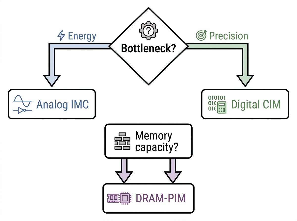
Measure the bottleneck. Determine whether the application is limited by memory bandwidth, latency, arithmetic throughput, capacity, or communication between devices.
Define the accuracy and precision contract. Record the required model quality, numeric formats, accumulation precision, and allowed calibration.
Map the full workload. Identify which operators run in memory, which run on the host, and how much data crosses the boundary.
Check capacity and update behavior. Confirm whether weights or data fit locally and how often they must be rewritten.
Inspect the software path. Test compiler coverage, unsupported-operator fallback, debugging, profiling, model conversion, and deployment APIs.
Normalize benchmarks. Compare at the same model, batch size, precision, accuracy, and power boundary.
Verify maturity. Distinguish simulation, silicon prototype, sampling, development system, full production, and independently deployed product.
Run a representative proof of concept. Measure end-to-end latency, throughput, energy, host utilization, accuracy, and engineering effort on real data.
Procurement verification checklist
Supported models, operators, data types, batch sizes, and sequence lengths
Usable memory capacity after redundancy, metadata, and model partitioning
Peak versus sustained throughput under the target accuracy requirement
Power measurement boundary and required host, memory, networking, and cooling
Toolchain version, framework support, licensing, and long-term maintenance
Calibration, retention, endurance, error handling, and environmental limits
Availability status, lead time, qualification evidence, and reference customers
Frequently asked questions
What is an in-memory computing chip?
It is a chip or memory-based platform that performs selected operations inside a memory array or close to stored data. The category includes analog CIM, digital CIM, DRAM-PIM, and near-memory architectures.
What is the difference between CIM and PIM?
CIM usually refers to operations performed within a memory array or its tightly coupled circuitry. PIM often refers to processing resources integrated in or near a memory device, bank, stack, or module. Vendor terminology overlaps, so the physical data path is more important than the label.
Are all in-memory computing chips analog?
No. Some designs use analog or mixed-signal crossbars, while others perform fully digital logic or arithmetic near SRAM or DRAM. Each approach has different precision, capacity, efficiency, and software tradeoffs.
Can in-memory computing replace a GPU?
Usually it acts as an accelerator rather than a complete replacement. A host CPU, GPU, or controller still handles unsupported operators, control flow, communication, preprocessing, and system management. The answer depends on workload coverage and software integration.
Can in-memory computing train AI models?
Research has demonstrated in-memory and analog training methods, but commercial activity is more concentrated on inference and data-intensive acceleration. Training requires accurate repeated weight updates, endurance management, and software support.
Which memory technology is best for CIM?
There is no universal best choice. SRAM offers mature, fast digital integration; DRAM offers capacity for PIM; ReRAM, PCM, and Flash can provide nonvolatile conductance states but introduce device and programming constraints. The workload and product maturity decide the practical fit.
How should TOPS/W claims be compared?
Use the same model, precision, batch size, sparsity, accuracy target, and power boundary. An array-only figure is not directly comparable with a complete chip or server result. Sustained application performance is more useful than an isolated peak number.
Is processing-in-memory commercially available?
Some PIM and digital in-memory platforms are commercially available, while others remain prototypes, demonstrations, samples, or early-production products. Confirm current availability, toolchain access, supported workloads, and customer qualification directly with the supplier.
Conclusion
In-memory computing is a family of architectures designed to reduce costly data movement. Analog CIM can exploit device physics for parallel matrix operations, digital CIM can bring predictable arithmetic into memory macros, and PIM can place programmable processing near high-capacity memory. None is automatically superior. The strongest evaluation combines workload profiling, accuracy requirements, capacity, peripheral overhead, software maturity, reliability, and current product status.
References
Nature Electronics: Computing-in-memory technologies and architectures for full-stack integration.
IBM Research: An analog-AI chip for energy-efficient speech recognition and transcription.
IBM Research: New algorithms may enable training AI models on analog chips.
Analog or Digital In-memory Computing? Benchmarking through Quantitative Modeling.
Samsung Semiconductor: HBM-PIM and Aquabolt-XL demonstration announcement.
UPMEM: processing-in-memory architecture and reference platform.
 UTMEL
UTMEL
We are the professional distributor of electronic components, providing a large variety of products to save you a lot of time, effort, and cost with our efficient self-customized service. careful order preparation fast delivery service
 Discovering New and Advanced Methodology for Determining the Dynamic Characterization of Wide Bandgap DevicesSaumitra Jagdale15 March 20242876
For a long era, silicon has stood out as the primary material for fabricating electronic devices due to its affordability, moderate efficiency, and performance capabilities. Despite its widespread use, silicon faces several limitations that render it unsuitable for applications involving high power and elevated temperatures. As technological advancements continue and the industry demands enhanced efficiency from devices, these limitations become increasingly vivid. In the quest for electronic devices that are more potent, efficient, and compact, wide bandgap materials are emerging as a dominant player. Their superiority over silicon in crucial aspects such as efficiency, higher junction temperatures, power density, thinner drift regions, and faster switching speeds positions them as the preferred materials for the future of power electronics.
Read More Applications of FPGAs in Artificial Intelligence: A Comprehensive GuideUTMEL29 August 20255581
This comprehensive guide explores FPGAs as powerful AI accelerators that offer distinct advantages over traditional GPUs and CPUs. FPGAs provide reconfigurable hardware that can be customized for specific AI workloads, delivering superior energy efficiency, ultra-low latency, and deterministic performance—particularly valuable for edge AI applications. While GPUs excel at parallel processing for training, FPGAs shine in inference tasks through their adaptability and power optimization. The document covers practical implementation challenges, including development complexity and resource constraints, while highlighting solutions like High-Level Synthesis tools and vendor-specific AI development suites from Intel and AMD/Xilinx. Real-world applications span telecommunications, healthcare, autonomous vehicles, and financial services, demonstrating FPGAs' versatility in mission-critical systems requiring real-time processing and minimal power consumption.
Read More The 2026 Engineer’s Guide: Choosing the Right MCU for Your Next IoT & New Energy ProjectUTMEL30 April 20261860
A comprehensive comparison of 2026's leading MCUs from ST, NXP, and Microchip across power efficiency, processing performance, connectivity, and ecosystems to help engineers select the optimal chip for next-gen IoT and new energy projects.
Read More AI Server Components: Engineering Next-Gen Data Center Hardware for 100kW RacksUTMEL15 May 20261003
The transition from traditional enterprise IT to AI-driven workloads has rendered legacy data center hardware obsolete, forcing infrastructure planners to re-engineer server components for extreme thermal environments.
Read More The Practical Engineer’s Guide to the NE555N Timer: Pinout, Setup, and TroubleshootingUTMEL29 May 2026797
This comprehensive guide explores the NE555N timer, detailing its 8-pin layout, internal architecture, and key datasheet specifications. It compares the bipolar IC to CMOS variants and details setup configurations for astable, monostable, and bistable modes. Additionally, the guide offers practical troubleshooting advice to prevent common breadboard failures, such as floating reset pins and electrical noise issues.
Read More
Subscribe to Utmel !
![AT88SC25616C-PU]() AT88SC25616C-PU
AT88SC25616C-PUMicrochip Technology
![FM3164-G]() FM3164-G
FM3164-GCypress Semiconductor Corp
![HCS301-I/P]() HCS301-I/P
HCS301-I/PMicrochip Technology
![L9660TR]() L9660TR
L9660TRSTMicroelectronics
![MOC3062VM]() MOC3062VM
MOC3062VMON Semiconductor
![MOC3020SR2M]() MOC3020SR2M
MOC3020SR2MON Semiconductor
![FGBS3040E1-F085]() FGBS3040E1-F085
FGBS3040E1-F085ON Semiconductor
![ATSHA204-TSU-T]() ATSHA204-TSU-T
ATSHA204-TSU-TMicrochip Technology
![AD8196ACPZ]() AD8196ACPZ
AD8196ACPZAnalog Devices Inc.
![TLE8110EDXUMA1]() TLE8110EDXUMA1
TLE8110EDXUMA1Infineon Technologies


