

 Product
 Brand
Brand Articles
 Tools
Tools
2nm vs 3nm Chips: What the Latest Process Nodes Mean for Performance
Quick Answer: The 2nm vs. 3nm Process-Node Divide
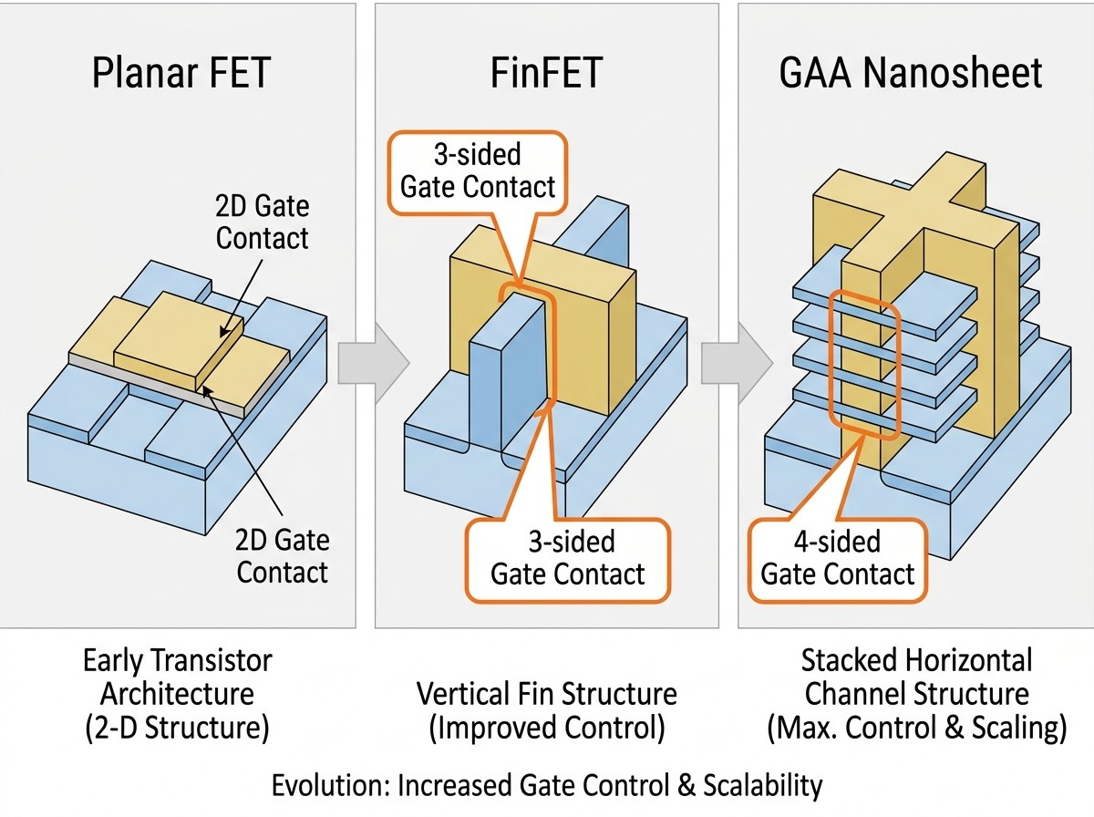
The shift from 3nm to 2nm is less about a one-nanometer shrink and more about a fundamental change in how transistors are built. Mainstream 3nm process nodes—such as TSMC N3E, N3P, and N3B—still rely on 3D FinFET structures, where the gate wraps around a vertical fin on three sides. Leading 2nm-class nodes move to Gate-All-Around (GAA) nanosheet transistors[4], where the gate surrounds a stacked horizontal channel on all four sides.
In practical terms, the generational targets that matter to chip architects and engineering teams are:
| Metric | What 2nm targets vs. standard 3nm baseline |
|---|---|
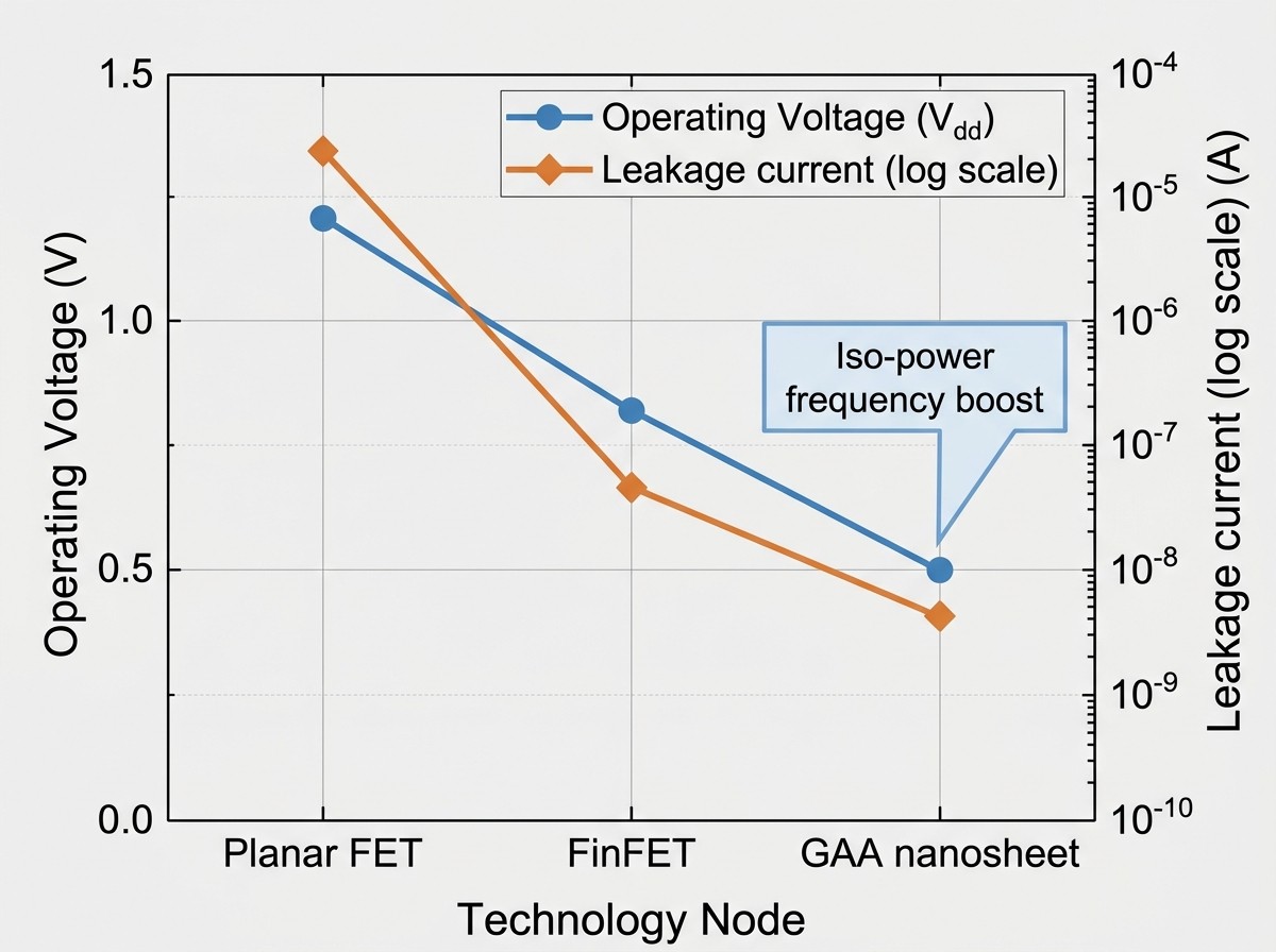
| Performance at iso-power | Approximately 10–15% higher clock frequency versus TSMC N3E (foundry design target) |
| Power at iso-frequency | Approximately 25–30% lower active switching power versus N3E (foundry design target) |
| Logic density | Roughly 1.15× (15%) density gain versus N3E (foundry design target) |
| Transistor architecture | GAA nanosheet (4-sided gate) vs. FinFET (3-sided gate) |
| SRAM cell area | ~0.0175 µm² on TSMC N2 vs. ~0.021 µm² at N5/N3E |
The caveat: these are foundry design targets, not guarantees for every chip. The real-world result depends on how the physical design team chooses to trade speed against power, which standard-cell libraries they use, and how much of the die is logic versus SRAM or I/O.
The Decision Framework at a Glance
Before diving into device physics and foundry roadmaps, here is the practical engineering and procurement boundary:
Target 2nm (2025–2027 ramp window)
Frontier AI training and inference accelerators where compute density, interconnect parasitics, and energy-per-operation dominate total cost of ownership.
High-frequency hyperscale server CPUs that need sustained clock headroom and can offset wafer premiums through rack-level power savings.
Thermally constrained ultra-flagship mobile SoCs where subthreshold leakage directly affects standby battery life and peak thermal throttling.
Standardize on 3nm (N3E / N3P / SF3)
Mainstream enterprise compute and cloud CPUs that can use mature PDKs, stable design rules, and chiplet-based partitioning.
High-volume mobile processors where tape-out economics and time-to-market matter more than a single-node density step.
Discrete GPUs and edge AI accelerators that benefit from mature FinFET toolchains and proven IP availability.
Retain 4nm or 5nm
Cost-sensitive consumer electronics, automotive safety controllers, and industrial IoT where functional-safety qualification timelines and long product lifecycles outweigh marginal density gains.
1. Demystifying Node Nomenclature: Why "2nm" Is Not 2 Nanometers
One of the most common misunderstandings in semiconductor coverage is treating "2nm" as a physical dimension. It is not.
Prior to the 22nm generation, process labels roughly tracked physical gate length or half-pitch. That correspondence broke down when the industry moved from planar transistors to 3D FinFETs. Today, process names are commercial designations that benchmark a node's expected power-performance-area generation relative to its predecessor.
At modern 3nm and 2nm nodes, physical scaling metrics remain far larger than the marketing name suggests. Standard contacts and interconnect pitches in this generation typically measure:
| Physical Parameter | Typical Range at 3nm/2nm-class Nodes |
|---|---|
| Contacted Poly Pitch (CPP) | Approximately 45–48 nm |
| Minimum Metal Pitch (MMP) | Approximately 20–24 nm |
These numbers come from industry roadmap work and published process-node documentation, not from foundry marketing pages. They matter because CPP and MMP—combined with standard-cell track height—determine real logic density.
Engineering takeaway: Never compare "3nm" from TSMC directly to "3nm" from Samsung or "Intel 3" without normalizing for cell track height, CPP, and MMP. The same marketing number can describe very different physical layouts and density characteristics across foundries.
2. Transistor Physics: FinFET vs. Gate-All-Around (GAAFET) Architecture
Why FinFET runs out of steam below 3nm
FinFETs solved the leakage and short-channel problems that plagued planar transistors by lifting the channel into a vertical fin and wrapping the gate around three sides. That structure worked well from roughly 22nm down through 5nm and into 3nm-class refinements.
But FinFET physics hits practical limits as dimensions contract further, including:
Drain-induced barrier lowering (DIBL): The gate's 3-sided wrap loses electrostatic control as the fin shrinks, making it harder to stop current when the transistor is supposed to be off.
Subthreshold leakage through the un-gated fin bottom: The bottom of the fin remains difficult for the gate to fully control, creating parasitic leakage paths.
Drive current quantization: FinFET designers must use integer fin counts—one fin, two fins, three fins—which constrains how finely a circuit can trade drive strength against power consumption.
How GAA nanosheets restore electrostatic control
GAA nanosheets replace the vertical fin with stacked horizontal channel layers, fully surrounded by the gate dielectric and metal gate on all four sides. This 360-degree channel encirclement does two critical things.
First, it restores steep subthreshold swing. A gate that surrounds the channel on all four sides exerts much better electrostatic authority than a gate touching only three sides, which means the transistor can switch with sharper on/off behavior and lower leakage.
Second, it eliminates the un-gated bottom-fin leakage path that plagued late-generation FinFETs. The entire channel is controlled.
Peer-reviewed device-physics literature, including MDPI[2] and ScienceDirect analyses[3], consistently identifies this 4-sided gate encirclement as the primary architectural mechanism that enables supply-voltage scaling to resume where FinFET flattened out. That voltage scaling is essential for power efficiency at smaller geometries.
Continuous nanosheet widths vs. discrete fin quantization
One underappreciated advantage of GAA nanosheets is design flexibility.
TSMC's N2 generation introduces a design methodology called NanoFlex, which allows cell-level mixing of short-channel and wide-channel nanosheets on the same die. Short-channel nanosheets optimize energy efficiency; wide-channel nanosheets deliver higher drive current. This replaces the rigid "how many fins" question with a continuous width modulation approach.
The practical result: physical design teams can fine-tune standard cells for speed or power far more precisely than was possible with quantized FinFET fins.
Architecture comparison
| Parameter | Planar FET (legacy nodes) | FinFET (3nm / 5nm) | GAA nanosheet FET (2nm class) |
|---|---|---|---|
| Gate-to-channel contact | 1 side | 3 sides | 4 sides (360°) |
| Channel orientation | Horizontal bulk silicon | Vertical fin | Stacked horizontal nanosheets |
| Drive-current tuning | Continuous planar width | Discrete fin counts | Continuous nanosheet width |
| Subthreshold leakage control | Poor | Moderate at ≤3nm | Superior |
| Short-channel effect suppression | Low | High | Higher |
3. Performance, Power, and Area (PPA): What the Benchmarks Actually Show
The cleanest public TSMC baseline for comparing 2nm against 3nm is N2 versus N3E. This is an intra-generational comparison, not a multi-node skip, which is important because many search results conflate the two.
TSMC's stated N2 design targets versus N3E are (vendor-published, not peer-reviewed):
| PPA Dimension | TSMC N2 Target vs. N3E |
|---|---|
| Iso-power speed improvement | 10–15% |
| Iso-frequency power reduction | 25–30% |
| Logic density scaling | ~1.15× (15%) |
These are foundry-specified design targets, not measured benchmarks from shipping chips. Real silicon will vary depending on how aggressively a design pushes frequency, how much leakage the team is willing to accept, and how much of the clock tree or power grid dominates the layout.
Why public answers disagree. Many articles and AI-generated summaries conflate the 5nm-to-3nm jump with the 3nm-to-2nm jump. The 5nm-to-3nm transition delivered much larger headline gains—often cited in the range of 25–45% power reduction depending on baseline and operating point—because it was a more substantial node step. The 2nm transition from a refined 3nm baseline is smaller in percentage terms but delivers meaningful gains across all three PPA axes.
The practical implication for engineering teams: treat 2nm as an incremental but important PPA improvement over refined 3nm, not as a generational leap equivalent to the 5nm-to-3nm transition.
4. The SRAM Scaling Wall and Thermal Density
What stalled SRAM means for architecture
Logic scales roughly 15% or more per node at 2nm. SRAM does not.
The 6-transistor (6T) SRAM bit-cell—the fundamental building block of on-die L1, L2, and L3 caches—has hit a physical scaling wall. Per published process documentation reviewed for this guide, high-density SRAM cell area remained at approximately 0.021 µm² through TSMC N5 and N3E. It shrinks to roughly 0.0175 µm² on TSMC N2, reaching a density of about 38.1 Mb/mm² — though these figures are subject to design-technology co-optimization (DTCO) details.
That is meaningful progress at the macro level through design-technology co-optimization (DTCO), but it lags far behind logic scaling. The consequence: for a fixed cache capacity, SRAM consumes a disproportionately larger share of die area at 2nm than it did at 5nm.
This single fact drives much of modern processor architecture:
Chiplet disaggregation: Put logic-heavy compute tiles on expensive 2nm wafers while keeping SRAM-heavy memory controllers and I/O on mature 4nm or 6nm nodes.
3D cache stacking: Direct hybrid-bonded vertical cache chips—such as AMD 3D V-Cache—bypass planar SRAM limits by moving capacity vertically.
Cache hierarchy redesign: Architects become more selective about cache capacities, favoring heterogeneous cache hierarchies over brute-force capacity expansion.
The thermal paradox
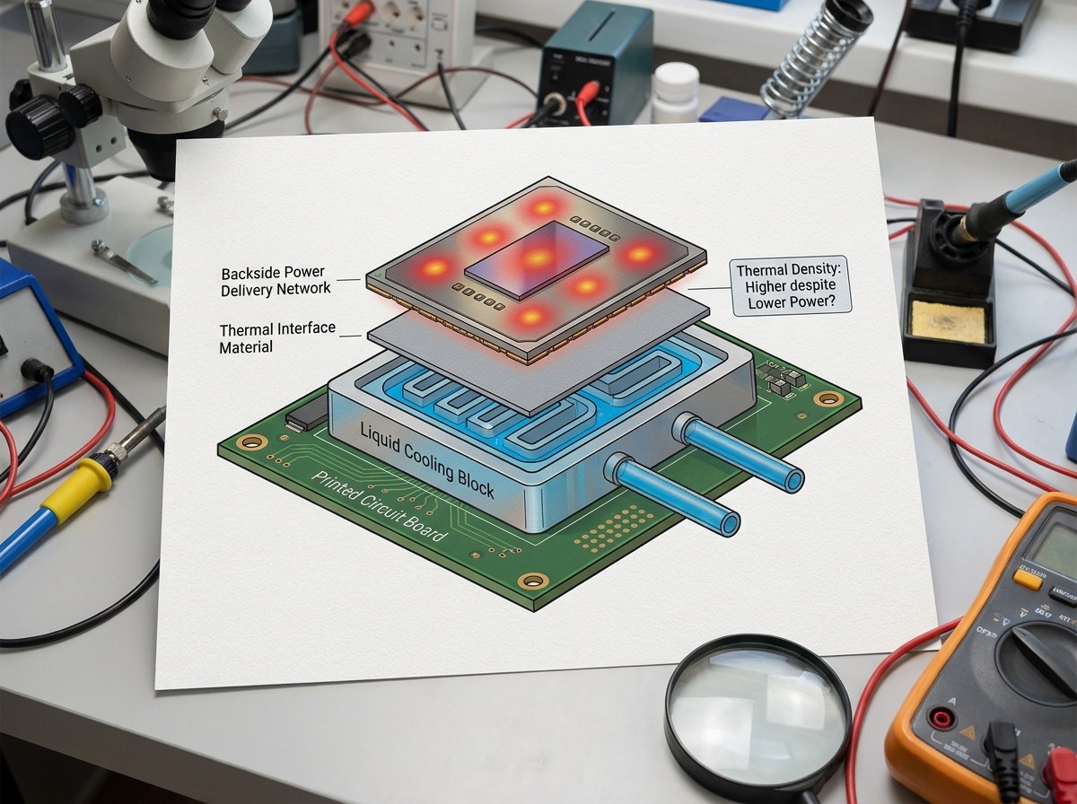
Less switched power per transistor does not always mean a cooler die. While dynamic switching energy per device falls at 2nm, transistor density rises faster than per-transistor power falls, pushing up localized power density—commonly expressed in W/mm².
GAA nanosheets add an extra wrinkle: the dielectric isolation layers surrounding the horizontal channel material have lower thermal conductivity than bulk silicon. The result is concentrated hotspots and more demanding thermal management requirements. Advanced liquid cooling, metal thermal interface materials, and aggressive package-level heat spreading become necessary for high-performance 2nm silicon.
The rule of thumb for engineering teams: total board-level power may drop, but that is not the same as thermal density dropping. Package thermal design must be re-evaluated at the node transition.
5. Backside Power Delivery Networks (BSPDN)
The problem: frontside wire congestion
In conventional chips, both power and signal wiring route across 15–20 metal layers on the frontside of the wafer. Power rails are thick, wide, and hungry for routing space. Signal wires benefit from narrow pitches but suffer when they must share routing resources with power.
The result is IR drop—voltage droop that degrades timing margins—and higher RC parasitics on signal interconnects as wire dimensions shrink.
The solution: moving power to the backside
Backside Power Delivery (BSPDN) relocates the power distribution network to the back of a thinned silicon die, connected through nano-scale through-silicon vias or direct-contact structures. This decouples the two wiring functions:
Frontside layers: Dedicated to high-speed signal routing.
Backside layers: Dedicated to low-resistance power delivery.
By separating power from signal, BSPDN reduces IR drop, reduces routing congestion, and can free up enough overhead to enable higher clock frequencies or lower dynamic power.
Foundry implementation divergence
Not all first-generation 2nm nodes include BSPDN. Implementation timing varies by foundry:
| Foundry | First-gen 2nm-class node | BSPDN timeline |
|---|---|---|
| Intel | 18A with RibbonFET + PowerVia | Integrated at first 18A ramp |
| TSMC | N2 with standard frontside power | N2P / A16 introduces Super Power Rail (SPR), late 2026 / 2027 |
| Samsung | SF2 with standard frontside power | SF2Z, targeted for 2027 |
TSMC's A16 positioning indicates Super Power Rail is expected to provide roughly 8–10% speed gain or 15–20% power reduction over N2P. Until that public roadmap becomes shipping silicon, treat these as foundry design targets.
The architectural takeaway: Intel is taking the early-integration path with PowerVia at its first 18A ramp. TSMC is sequencing BSPDN into its A16 generation. Samsung is following with SF2Z. If backside power delivery is central to your design, the node selection decision is equally about timing as it is about architecture.
6. Foundry Showdown: TSMC N2 vs. Samsung SF2 vs. Intel 18A
The major foundries have taken different routes to 2nm-class silicon, and they use different commercial names for the same underlying GAA concept.
| Foundry & Node | Transistor Architecture | Power Delivery | Production Milestone |
|---|---|---|---|
| TSMC N2 / N2P | Nanosheet GAA with NanoFlex | Frontside on N2; BSPDN on N2P/A16 | Volume production late 2025, with expanded output at Baoshan and Kaohsiung fabs |
| Samsung SF2 / SF2Z | MBCFET (Multi-Bridge-Channel FET) | Frontside on SF2; BSPDN on SF2Z | SF2 ramp targeted 2025/2026, with SF2P in 2027 and SF1.4 in 2029 on the roadmap |
| Intel 18A | RibbonFET GAA | PowerVia BSPDN at first ramp | Late 2025/2026 ramp |
The nomenclature difference—Nanosheet, MBCFET, RibbonFET—reflects branding distinctions, not fundamentally different device physics. All three implement the same core idea: stacked horizontal nanosheets enveloped by a 4-sided gate.
Strengths and drawbacks
TSMC N2
Strength: Mature EDA ecosystem, established high-volume manufacturing, and a wide IP portfolio from third-party providers.
Drawback: Backside power delivery deferred to A16/N2P generation; high wafer pricing pressure.
Best for: Fabless hyperscalers and flagship mobile chip teams that need production scale and low design-risk.
Samsung SF2
Strength: Accumulated GAA learning from early MBCFET deployment at its 3nm generation.
Drawback: Slower third-party IP and EDA ecosystem integration than TSMC.
Best for: Cost-conscious custom silicon programs and Samsung internal mobile SoC designs.
Intel 18A
Strength: Earliest integration of BSPDN via PowerVia alongside RibbonFET GAA; aggressive performance-per-watt targets.
Drawback: Foundry customer ecosystem (IFS) still less proven than TSMC's external design ecosystem.
Best for: High-frequency enterprise and HPC architectures, especially designs that value early backside power integration.
Why rankings and yield rumors disagree. Much of the public discourse around "who wins" 2nm relies on unverified yield percentages circulating in analyst notes and social channels. Those numbers are unverified analyst estimates that have not been confirmed by foundry disclosures and should not drive procurement decisions. Yield ramps are defect-density learning curves, not static scores, and they vary by die architecture, defect tolerance, and maturity of the specific production line.
7. Economic Trade-Offs: Who Needs 2nm vs. Who Should Stay on 3nm?
The primary economic driver at 2nm is not wafer cost alone—it is cost per good die, multiplied by the operational energy saved at system scale. For some workloads, the equation flips decisively in favor of 2nm. For others, the premium does not justify the transition.
| Application / Workload | Node Strategy | Technical Justification | Trade-off |
|---|---|---|---|
| Frontier AI training and LLM inference | 2nm (N2 or 18A) | Compute density, interconnect performance, and energy-per-operation matter more than wafer cost | Accepts node premium because energy savings compound at rack scale |
| Flagship mobile SoCs | 2nm (N2 or SF2) | Sub-5W handheld thermal limits and battery life directly benefit from leakage reduction | High unit volume amortizes mask and EDA investment |
| Enterprise server and cloud CPUs | 3nm (N3P) or hybrid 2nm chiplets | Chiplet architecture lets compute tiles use 2nm while SRAM and I/O stay on mature nodes | Optimizes total die cost without sacrificing compute gains |
| Mid-tier mobile and edge AI | 3nm (N3E) or 4nm | Mature PDKs, stable supply, insufficient end-user benefit at 2nm to justify premium | Keeps total product cost in line with launch timelines |
| Automotive and industrial | 3nm, 4nm, or 5nm | Functional-safety qualification and long production lifecycles favor mature FinFET nodes | Proven reliability and AEC-Q100 processes reduce risk |
Hidden economic risks at 2nm
EDA toolchain complexity. GAA design rules are new. Verified design flows and fully qualified SPICE models may not yet exist for all IP blocks.
SRAM economics. Large on-die caches at 2nm cost disproportionate die area. Teams without a chiplet or 3D-cache strategy may see total silicon costs rise faster than expected.
Thermal budget shifts. Backside power delivery changes thermal paths. Thermal sign-off models must be re-validated for the new physical stack.
IP ecosystem gaps. Mature third-party IP for PCIe, DDR, and UCIe interconnects may lag first-generation 2nm PDMs. None of these are guaranteed replacements until the IP passes integration sign-off.
8. Frequently Asked Questions
Why did TSMC keep FinFET for 3nm while Samsung switched to GAA at 3nm?
TSMC chose to maximize node maturity and commercial delivery by pushing FinFET to its practical limit across N3B, N3E, and N3P. Samsung absorbed its GAA/MBCFET learning curve earlier, at 3nm, to gain production experience before the 2nm generation. Both strategies flow into the same endpoint: TSMC adopts nanosheet GAA at N2, while Samsung refines MBCFET into SF2.
Can scaling continue past 2nm?
Yes. The industry roadmap extends into Angstrom-era nodes—1.4nm-class and 1.0nm-class designations—with further architectural changes. The next major transistor evolution after horizontal GAA nanosheets is the complementary FET (CFET), which vertically stacks nMOS and pMOS transistors. Advanced 2D channel materials and High-NA EUV lithography are part of that long-term path.
What is the difference between GAAFET, MBCFET, RibbonFET, and nanosheets?
They are foundry-specific commercial names for the same core architecture: stacked horizontal nanosheet transistors surrounded on all four sides by the gate. TSMC calls its implementation nanosheet GAA; Samsung brands it MBCFET; Intel uses RibbonFET. The labels differ; the underlying device physics does not.
How does 2nm affect smartphone battery life versus data center power consumption?
In smartphones, 2nm reduces static leakage during idle and light workloads, improving standby time and reducing thermal throttling under burst loads. In data centers, the 25–30% active power reduction at matched frequency means more compute can be packed into a fixed power and cooling envelope, which translates into lower operational energy per workload.
9. Hardware Engineering and Sourcing Checklist
Before a team commits to a 2nm tape-out or hardware refresh, verify these items:
EDA toolchain readiness. Confirm physical design flows support GAA variable nanosheet DRC and mixed-width standard cells such as NanoFlex.
PDK maturity. Ensure the foundry process design kit is at version 1.0 or higher with fully qualified SPICE models for target operating corners.
Third-party IP availability. Verify that PCIe, DDR, and UCIe blocks are hardened and characterized for the specific 2nm-class node. Treat vendor roadmaps as candidates to validate, not guaranteed replacements.
Thermal and packaging plan. Re-sample thermal simulations against projected localized power density and confirm that proposed TIM, heat spreader, or liquid cooling solutions match the package thermal resistance budget.
SRAM partitioning strategy. Decide whether large cache blocks move to 3D stacked dies or off-die chiplets, or whether cache capacity must shrink to control die area.
Backside power design sign-off. If targeting Intel 18A or TSMC A16, verify that the CAD flow handles backside TSV floorplanning, voltage drop analysis, and backside thermal modeling.
Yield and maturity assumptions. Do not base tape-out decisions on leaked yield percentages or secondhand analyst estimates. Treat yield as a ramp curve that improves with each process revision, and demand foundry-verified defect-density data under NDA.
TSMC 5nm, 3nm and 2nm devices explained | Technology Node | VLSI | Why such naming? | TSMC
Sources and references used for this guide
3nm Technology - TSMC
Source type: official company documentation
Used for: TSMC N3/N3E official logic density, power efficiency, and performance scaling specifications against N5.
Caution: Vendor source; represents foundry target specifications and design rules.A Review of the Gate-All-Around Nanosheet FET Process Opportunities
Source type: research source
Used for: Transistor device physics, FinFET vs GAAFET channel electrostatics, subthreshold swing, and short-channel effect mitigation.
Caution: Academic research paper; focuses on physical mechanisms rather than commercial foundry schedules.Exploring optimal TMDC multi-channel GAA-FET architectures
Source type: research source
Used for: Carrier mobility, multi-channel nanosheet electrostatic control, and quantum leakage suppression at sub-3nm scales.
Caution: Theoretical and experimental simulation data for advanced channel materials.What are Gate-All-Around (GAA) Transistors?
Source type: reputable professional source
Used for: EDA design perspectives, continuous nanosheet width variation vs discrete fin quantization, and standard cell optimization.
Caution: EDA tool vendor perspective; highly accurate on cell layout design rules.TSMC N2 vs Intel 18A vs Samsung SF2 Wiki
Source type: reputable professional source
Used for: Comparative node analysis across TSMC, Samsung, and Intel 2nm-class architectures, transistor densities, and power delivery roadmaps.
Caution: Industry analysis based on public disclosures and reverse-engineering models.Entering the nanosheet transistor era
Source type: industry institution
Used for: Semiconductor roadmap evolution from FinFET to Nanosheet, Forksheet, CFET, and Backside Power Delivery networks.
Caution: Pre-competitive research roadmap; commercial execution timelines vary by foundry.From FinFET to GAA: Samsung's fab journey to 3nm and 2nm
Source type: reputable professional source
Used for: Samsung's early adoption of Multi-Bridge-Channel FET (MBCFET) GAA architecture at the 3nm and 2nm nodes.
Caution: Covers Samsung foundry strategy and technical milestones.Leading-edge foundry roadmaps for TSMC, Intel and Samsung
Source type: reputable professional source
Used for: Timeline tracking of high-volume manufacturing (HVM) schedules for TSMC N2, Intel 18A, and Samsung SF2.
Caution: Journalistic compilation of roadmap targets subject to fab construction and yield ramp shifts.
 UTMEL
UTMEL
We are the professional distributor of electronic components, providing a large variety of products to save you a lot of time, effort, and cost with our efficient self-customized service. careful order preparation fast delivery service
 Improving the Energy Conversion Efficiency of Triboelectric NanogeneratorsSaumitra Jagdale19 November 20243256
There is a huge growth in demand for self-sustaining electronic devices, as the traditional power-generating devices fail in remote and harsh environments due to the periodic requirement of battery changes. Also, these devices are frequency specific; some work only in high frequency and some in low frequency. Triboelectric nanogenerators (TENGs) provide a promising solution by efficiently converting mechanical energy into electricity as they are versatile, compact, and cheap, making them a popular choice.
Read More Methodologies for Increasing Efficiency of Fuel Stack Technology for Energy GenerationSaumitra Jagdale19 November 20243102
Presently, power companies are moving towards renewable energy systems. Conventional energy sources are more expensive because they require a vast network to be maintained and huge human resources. Also, they harm the environment by releasing several harmful gases. As the industry’s focus shifts toward renewable energy sources, energy systems powered by Proton Exchange Membrane Fuel Stacks (PEMFS) are gaining traction.
Read More VSC Light Meaning, Causes, and Step-by-Step DiagnosticsUTMEL19 May 20263491
A VSC (Vehicle Stability Control) light indicates the system is disabled, often as a fail-safe triggered by unrelated engine faults like a loose gas cap. While the stability system prevents lateral skidding, it shuts down when sensor data is unreliable. Proper diagnosis requires an ABS-capable OBD2 scanner. Resolving the root engine code, checking wheel speed sensors, or performing a zero-point calibration usually restores system function.
Read More What JEDEC JEP203 and JEP204 Actually Change for SiC Qualification Engineers and Component BuyersUTMEL29 July 2026481
Summary: When JEDEC published JEP203 and JEP204 on June 3, 2026[1], most coverage treated them as an announcement. They are better understood as the first shared language the silicon carbide industry has had for two problems that have quietly consumed engineering hours since the first commercial SiC MOSFETs shipped: short-circuit evaluation that produces numbers you can compare across suppliers, and a consolidated reference of stress procedures so qualification engineers stop reinventing test plans from scratch. This article explains what changes on Monday morning and what to ask suppliers for now.
Read More 2nm vs 3nm Chips: What the Latest Process Nodes Mean for PerformanceUTMEL19 August 20261572
The shift from 3nm to 2nm process nodes marks a fundamental change in transistor architecture, moving from FinFET to Gate-All-Around (GAA) nanosheets. This transition delivers meaningful improvements in performance, power, and density, but also introduces new challenges like SRAM scaling limits, thermal density, and backside power delivery. The article compares TSMC, Samsung, and Intel approaches, offering a practical decision framework for engineering teams.
Read More
Subscribe to Utmel !
![H-806R-UV]()
![3443-82-08]()
![Z80-259]() Z80-259
Z80-259Harwin Inc.
![21792]() 21792
217923M
![1212266]() 1212266
1212266Phoenix Contact
![28896]() 28896
28896Wiha
![2912584-01]() 2912584-01
2912584-01Stewart Connector
![72923-2]() 72923-2
72923-2Pomona Electronics
![FLCFPLF-X]() FLCFPLF-X
FLCFPLF-XPanduit Corp
![0153-01-INS]() 0153-01-INS
0153-01-INSGreenlee Communications


