Product
 Brand
Brand Articles
 Tools
Tools
Semiconductor PCN Review Checklist: From Notification to Engineering Sign-Off
A semiconductor Product Change Notification (PCN) is an engineering risk event, not an administrative update. When an Integrated Device Manufacturer (IDM) or foundry alters a fabrication site, package chemistry, bonding metallurgy, or silicon mask set, treating the vendor’s "drop-in compatible" claim as a rubber stamp invites assembly line shutdowns, field reliability failures, and unbudgeted redesigns.
Managing semiconductor PCNs requires a structured delta-qualification review that maps supplier-level change mechanisms directly to system-level application stress.
Quick Answer: The 5-Minute PCN Triage Protocol
Incoming PCNs must be triaged within 48 hours of receipt to prevent contractual auto-acceptance. Major semiconductor manufacturers enforce commercial terms of sale under which an unacknowledged notification defaults to customer approval within 30 calendar days.
When a notification arrives in your engineering or procurement inbox, execute this immediate four-step triage:
Step 1: Direct MPN and Where-Used Lookup (Hour 0–12)
Query the affected Manufacturer Part Number (MPN) against your active enterprise Resource Planning (ERP) and Product Lifecycle Management (PLM) databases. Identify every top-level Bill of Materials (BOM), active production site, and open Purchase Order (PO). If the part is not in an active or planned production BOM, archive the notice for traceability and close the ticket.Step 2: Contractual Clock and Cutover Log (Hour 12–24)
Record the official notification issue date. Calculate two non-negotiable milestones: the 30-day technical feedback/sample request deadline and the supplier’s proposed first ship date (FSD) (historically targeted at 90 days under industry baselines). Flag open purchase orders to prevent early, unauthorized shipment of changed material.Step 3: Change Vector and Severity Classification (Hour 24–36)
Scan the notification package to determine if the change is Major (impacting form, fit, function, quality, or reliability) or Minor (cosmetic, label, packing material). Major changes—such as wafer fab transfers, copper wire conversions, silicon stepping revisions, or automated test equipment (ATE) site shifts—require technical qualification.Step 4: Cross-Functional Routing (Hour 36–48)
Simultaneously issue task assignments to:Component Engineering: Form, fit, function, timing, and datasheet delta audit.
Supplier Quality Engineering (SQE): Reliability stress data audit and failure mechanism analysis.
Procurement / Sourcing: Buffer stock calculation, last-time-buy (LTB) of unchanged material, and cutover date-code tracking.
Fast-Track vs. Full Re-Qualification Decision Logic
ROUTE A: Administrative Fast-Track Closure
Criteria: The change involves only packing tray modifications, barcode label revisions, or pin-one tape-and-reel orientation that complies with existing EIA standards.
Action: SQE and Sourcing sign off. Notify incoming inspection; no electrical or reliability bench validation required.ROUTE B: Standard Delta-Qualification Gate
Criteria: The change involves assembly site moves, mold compound replacements, or pin-compatible ATE test location transfers with complete delta qualification reports provided.
Action: Audit supplier reliability data against industry standards. If data meets zero-defect criteria, perform physical sample dimensional and solderability checks before engineering release.ROUTE C: Deep-Dive Containment and Lab Validation
Criteria: The change involves front-end wafer fab transfers, die shrinks, silicon mask stepping revisions, or wire-bond metallurgy transitions (e.g., Gold to Copper).
Action: Freeze automatic acceptance via an official written hold letter. Order engineering samples, commission bench characterization across temperature extremes, and audit supplier stress-test sample sizes (, zero failures).
The Regulatory and Standards Framework: J-STD-046, JESD46, and ZVEI DeQuMa
Semiconductor change notifications are governed by voluntary consensus standards developed by the microelectronics industry to establish predictability across global supply chains.

Evolution from JESD46 to J-STD-046
Historically, solid-state component modifications were governed by JEDEC standard JESD46[2] (Customer Notification of Product/Process Changes by Solid-State Suppliers). To unify requirements across passive components, active solid-state devices, and integrated electronic assemblies, JEDEC and the Electronic Components Industry Association (ECIA) established J-STD-046[1] (and subsequent revisions including J-STD-046A).
J-STD-046 defines the minimum requirements for notifying customers when a supplier plans a "Major Change." A Major Change is defined as any alteration to an electronic product that can reasonably be expected to affect:
Form: The device's physical dimensions, footprint, mass, package geometry, or mechanical interface.
Fit: The physical or environmental interface with the customer's assembly (e.g., terminal finish, coplanarity, thermal resistance).
Function: The electrical, optical, thermal, or mechanical performance of the product over its operating conditions.
Quality or Reliability: The manufactured integrity, expected failure rate, or operating lifetime under operating mission profiles.
The 90-Day Advance Notification Baseline vs. 30-Day Tacit Acceptance
Under J-STD-046, suppliers must issue formal notification at least 90 days prior to the planned first shipment[4] of the modified product. This advance window is intended to give systems manufacturers sufficient runway to review documentation, acquire qualification samples, and complete system testing.
However, an operational trap exists within standard commercial terms of sale: the 30-day customer response window.
Major IDMs explicitly include clauses stating that if a customer does not submit a formal, written technical inquiry, sample request, or objection within 30 days of the notification date[6], the change is contractually deemed accepted.
Silence equals tacit approval. If an OEM engineering department lets an email sit unreviewed for five weeks, the supplier's ERP system automatically marks the account as cleared, releasing the modified components into standard production shipments once the 90-day window expires.
Note on Legal Force: J-STD-046 is a voluntary consensus standard, not a statutory law. Its enforcement is driven entirely by purchase agreements, supplier terms of sale, and bilateral quality contracts. In safety-critical sectors (such as automotive, avionics, and medical devices), bilateral Master Supply Agreements (MSAs) or Quality Assurance Agreements (QAAs) often mandate 180-day notification minimums and prohibit shipment without an explicit, signed Part Submission Warrant (PSW) or customer Engineering Change Order (ECO).
The ZVEI Delta Qualification Matrix (DeQuMa)
To eliminate ambiguity regarding which stress tests are technically required when a part changes, the German Electrical and Electronic Manufacturers' Association (ZVEI) created the Delta Qualification Matrix (DeQuMa).
Now recognized across global automotive and industrial electronics sectors, DeQuMa standardizes change notifications[8] by breaking modifications down into precise change numbers across semiconductors (SEMI), passive components (PASS), and MEMS sensors. Component and quality teams should periodically benchmark internal checklists against current matrix releases (such as DeQuMa Revision 5.0) as packaging technologies evolve.
Rather than allowing a supplier to determine testing ad hoc, DeQuMa identifies the physical risk vector—such as a wafer diameter shift or leadframe plating change—and cross-references the required qualification matrix (stress tests, sample sizes, and duration) required to validate that specific delta.
Operational Boundaries: Semiconductor PCN vs. PDN/EOL
A critical breakdown in manufacturing operations occurs when procurement and engineering conflate a Product Change Notification (PCN) with a Product Discontinuation Notice (PDN), also known as an End-of-Life (EOL) announcement.
Treating a PCN as an EOL notice results in unnecessary last-time-buy capital expenditure, while treating a PDN as a simple process change causes unrecoverable component obsolescence.
| Operational Dimension | Product Change Notification (PCN) | Product Discontinuation Notice (PDN / EOL) |
|---|---|---|
| Primary Industry Standard | J-STD-046 | J-STD-048 |
| Operational Intent | Ensure ongoing supply continuity under a modified manufacturing, material, or test baseline. | Formal termination of product manufacturing and commercial lifecycle. |
| Supply Continuity | Continuous: Part continues production under the same or revised ordering code. | Terminal: Part production permanently ceases after final manufacturing runs. |
| Primary Action Required | Technical Requalification: Delta qualification, bench validation, schematic/layout check, ECO release. | Supply Chain Securing: Total lifecycle demand forecasting, Last-Time-Buy (LTB), or alternate redesign. |
| Lead Department | Engineering & Supplier Quality: Component Engineer, SQE, Hardware Architect. | Procurement & Supply Chain: Strategic Sourcing, Financial Planning, Inventory Manager. |
| Standard Industry Timelines | Minimum 90 days notice before first shipment; 30-day technical response window. | Minimum 6 months from notice to place LTB orders; additional 6 months to accept final shipments (Last-Time-Ship / LTS). |
| Inventory Impact | Strategic bridge/safety stock to cover testing lead times and qualification margin. | Terminal volume purchase requiring significant capital allocation, inventory holding, and shelf-life monitoring. |
When a PCN is issued, the manufacturing process is evolving; engineering must verify that the product's behavior in their system remains unchanged. When a PDN is issued under J-STD-048, the component is dying; supply chain teams must secure remaining inventory while engineering identifies and qualifies an alternate footprint or pin-compatible candidate.
The 4 Core Semiconductor Change Categories & Physical Failure Vectors
Semiconductor qualification cannot be handled as a generic checklist. Different physical modifications introduce distinct electrical and mechanical failure mechanisms.
Reviewing engineers must audit the supplier's qualification test summary against the physical stress vectors specific to each change category.
Semiconductor Reliability Testing (10 Minutes)
1. Wafer Fabrication Site Transfers & Process Shrinks
Front-end changes involve transferring production to a new foundry, a different geographic fab, an expanded wafer diameter (e.g.,to), or a smaller lithography node (die shrink).
Physical & Silicon Phenomena
Transconductance and Threshold Voltage Drift: Variations in gate oxide thickness (), channel doping profiles, and gate length () shift threshold voltage () and transconductance (). In analog and mixed-signal components, this manifests as reference voltage drift, operational amplifier offset changes, or comparator threshold shifts.
Leakage Current (/): Thinner dielectric layers and shortened channel lengths increase sub-threshold leakage, dramatically elevating standby power consumption in battery-operated systems.
Parasitic Latch-Up: Substrate resistivity variations and layout alterations can reduce the trigger voltage or holding current of parasitic PNPN silicon-controlled rectifier (SCR) structures, increasing susceptibility to latch-up during power-rail transients.
Supplier Qualification Audit Checklist
Verify High-Temperature Operating Life (HTOL) testing executed per JESD22-A108. The baseline standard requires(or an equivalent accelerated stress temperature calculated via the Arrhenius equation).
Verify Statistical Process Capability: Demandfor general electrical parameters andfor critical parameters[5] (representing an expected defect rate under 0.6 DPPM) on key DC parametric distributions.
Verify Early Life Failure Rate (ELFR) burn-in data to confirm infant mortality rates are contained.
Require full Electrostatic Discharge (ESD) re-characterization: Human Body Model (HBM per JS-001) and Charged Device Model (CDM per JS-002), alongside Latch-Up testing per JESD78.
2. Packaging Materials & Assembly Site Moves
Back-end assembly modifications include changing the Outsourced Semiconductor Assembly and Test (OSAT) facility, shifting epoxy mold compound (EMC), changing die-attach adhesives, or altering bond-wire metallurgy.
Physical & Mechanical Phenomena
Coefficient of Thermal Expansion (CTE) Mismatches: Differences between the thermal expansion rates of the silicon die, copper leadframe, and mold compound induce mechanical stress during reflow soldering. This can cause package warpage, internal delamination, or broken passivations.
Die Attach Voiding and Thermal Runaway: An improper die-attach process or altered adhesive viscosity increases voiding beneath the die. This impedes heat flow to the exposed thermal pad, elevating junction-to-case thermal resistance () and triggering localized thermal runaways under sustained power loads.
Moisture Sensitivity Level (MSL) Degradation: Shifts in epoxy mold chemistry or leadframe adhesion can increase hygroscopic absorption, degrading the package from MSL 1 (unlimited floor life) to MSL 3 (floor life) and risking package "popcorning" during surface-mount reflow.
The Gold (Au) to Copper (Cu) Bond Wire Transition Hazard
To reduce cost, manufacturers frequently replace traditional gold wire bonds with pure copper (Cu) or palladium-coated copper (PCC). While electrically conductive and thermally efficient, copper wire is significantly harder than gold.
Pad Cratering Risk: Bonding copper wire requires higher ultrasonic energy and mechanical down-force during the ball-bonding process. This mechanical shock can generate micro-cracks in the fragile Inter-Layer Dielectric (ILD) layers beneath the bond pad—a failure mode known as pad cratering. These micro-fractures often pass factory automated testing, only to propagate into open circuits under thermal cycling in the field.
Intermetallic Corrosion: Copper-aluminum interfaces form intermetallic compounds (IMCs) that are highly susceptible to corrosion in the presence of trace halogens and moisture.
Supplier Qualification Audit Checklist
Verify Biased Highly Accelerated Stress Testing (bHAST) per JESD22-A110 (under bias voltage) or Temperature Humidity Bias (THB per JESD22-A101) to evaluate corrosion resistance as outlined in standard copper wire qualification delta qualification matrices[7].
Audit Temperature Cycling (TC) per JESD22-A104 (typically 500 to 1,000 cycles fromor).
Inspect Scanning Acoustic Microscopy (C-SAM) images. Verify zero delamination along the die surface, active wire bonds, and the die paddle.
For Cu-wire conversions, demand destructive cross-sectional analysis and wire-pull / ball-shear statistical distributions to confirm absence of pad cratering and sufficient intermetallic coverage.
3. Test Location & Platform Shifting
Transferring wafer probe or final package testing to an alternate OSAT facility or shifting across ATE platforms (such as from an Advantest tester to a Teradyne tester) is often dismissed as a minor risk. In practice, it represents a frequent source of field line escapes.
Operational & Yield Phenomena
Socket and Contactor Inductance: Alternate test sockets exhibit different parasitic inductances, contact resistances, and thermal dissipation traits. A device that comfortably passes high-frequency or high-current tests on one test fixture may oscillate or register false margins on another.
Tester Guard-Band Erosion: Different ATE platforms feature subtle discrepancies in instrument timing accuracy, ADC reference voltages, and voltage-forcing noise floors. If the supplier relaxes test guard-bands to compensate for tester noise, marginal silicon will ship to customers, resulting in customer line fallout (DPPM spikes).
Supplier Qualification Audit Checklist
Review the supplier’s Test Correlation Study: Demand side-by-side parametric yield correlation across a minimum of three production lots tested on both the original and transferred test platforms.
Audit Gage Repeatability and Reproducibility (Gage R&R) data for critical DC and AC datasheet parameters, ensuring measurement system variation consumes less than 10% to 20% of the total tolerance band.
Confirm test program parity: Verify that fault coverage, vector depth, and burn-in screening algorithms are identical.
4. Die Revisions & Silicon Steppings (Shrinks & Errata Fixes)
When an IC vendor releases a new silicon stepping (e.g., stepping A2 to B0) to patch internal circuit bugs or implement subtle layout improvements, they frequently assert 100% pin and functional compatibility. However, changes at the silicon level routinely alter dynamic circuit behavior.
Electrical & Firmware Phenomena
Edge-Rate Acceleration (): A die shrink or revised driver stage frequently sharpens output rise and fall times. Faster switching edges inject high-frequency harmonic energy into printed circuit board (PCB) traces, degrading radiated emissions (EMC) and inducing crosstalk on adjacent signal lines.
Timing Margin Collapse: Faster internal logic propagation shortens setup and hold times, potentially violating asynchronous timing windows or race conditions in external SPI, I2C, or parallel memory buses.
Silicon Errata Reversals: If your software architecture incorporated an intentional driver workaround for a known hardware bug in stepping A2, "fixing" that bug in stepping B0 can cause the driver workaround to fail, causing system hangs or initialization timeouts.
Supplier Qualification Audit Checklist
Request a complete AC/DC Characterization Delta Table, verifying propagation delays, drive strength, and input threshold levels across minimum, typical, and maximum operating corners.
Examine the updated Silicon Errata Sheet side-by-side with previous revisions.
Audit power-on reset (POR) trip thresholds and internal supply ramp-up profiles.
Industry Misconceptions and Flawed Review Practices
Reviewing semiconductor PCNs requires cutting through standard supplier assurances and avoiding internal shortcuts that leave systems vulnerable.
Fallacy 1: "Drop-In Compatible" Means Zero Internal Testing
Component datasheets only guarantee parameters specified within their min/max tables under static test conditions. They do not—and cannot—characterize every nuance of your specific circuit implementation. A replacement IC marketed as a "drop-in replacement" may exhibit different analog transient settling times, varied input impedance during power-up, or different decoupling requirements.
Vendor drop-in claims simply mean the component meets nominal footprint and baseline datasheet specifications; they do not guarantee dynamic interoperability in your production system.
Fallacy 2: Silence is Safe
Letting an ambiguous PCN lapse without an acknowledgment is an operational failure. In the eyes of component suppliers, distributors, and contract manufacturers, an unacknowledged PCN is an approved PCN once the 30-day window expires. Once approved, the supplier’s order management system is free to mix or substitute old and new revisions on open purchase orders without advance notice.
Fallacy 3: The Blanket 1,000-Hour Requalification Myth
Engineering teams sometimes swing to the opposite extreme, demanding that a supplier run a custom, full 1,000-hour HTOL or 1,000-cycle thermal test for minor packaging or test site moves.
This approach wastes engineering bandwidth and stalls product deliveries. Stress testing must follow the ZVEI DeQuMa framework: match the qualification test to the specific physical failure mechanism. If a test site moves, 1,000 hours of thermal stress proves nothing about tester socket correlation; a rigorous Gage R&R and dual-pass spike check is what actually validates test fidelity.
Fallacy 4: Treating Solder Fatigue as Internal Wire Integrity
Engineers frequently conflate board-level solder joint reliability (the physical SMT connection between the package leads and the PCB pad) with internal package reliability (the die-attach, substrate, and internal bond wires). Both fail under thermal stress, but their mechanics are entirely separate.
Board-level reliability depends on solder alloy, reflow profiles, PCB surface finishes, and board flexure. Internal package reliability depends on mold chemistry, silicon passivation, and wire-bond intermetallic compounds. Passing a board-level thermal cycle does not prove an internal copper-wire bond pad has avoided sub-surface dielectric cracking.
The Mandatory Role of Failure Analysis (FA)
If a device exhibits an anomaly during a qualification stress test, a supplier cannot simply dismiss it as a handling defect or a statistical outlier. Rigorous component review demands a comprehensive Failure Analysis (FA) report.
This analysis must utilize non-destructive scanning acoustic microscopy (C-SAM), high-resolution X-ray inspection, real-time micro-probing, precision cross-sectioning, and chemical decapsulation to determine the root cause. If the failure mechanism is tied to the newly introduced process, the PCN must be formally rejected.
Master Cross-Functional PCN Review Checklist & Responsibility Matrix
An effective review process requires unambiguous cross-functional ownership. The following operational table defines the sign-off gates from initial receipt to ERP cutover.
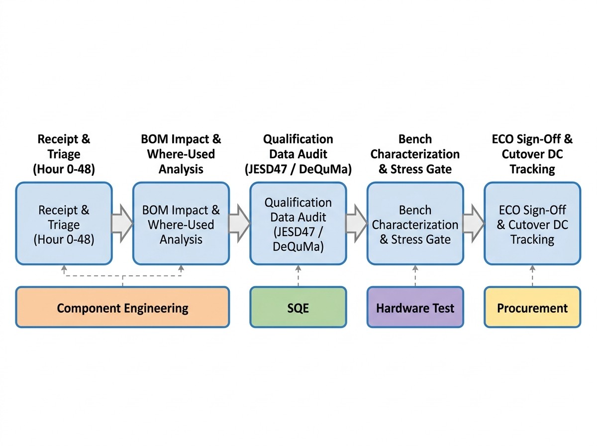
| Affected MPN | Internal BOM & Impacted Projects | Change Category & Severity | Required Supplier Evidence (Audit Gate) | Internal Hardware Validation Items | Target Cutover Date & First Lot/Date Code | Responsible Owner |
|---|---|---|---|---|---|---|
| STM32F407VET6 | BOM-10492: Industrial Gateway (Rev C); BOM-10883: Motor Controller (Rev B) | Wafer Fab Transfer: Expansion to secondary 300mm fab line (Major) | - AEC-Q100/JESD47 Qual Report[3] - 3 lots77 units HTOL (1,000h @ 125°C, 0 failures) -on core clock & ADC DNL/INL distributions | - Automated firmware regression suite execution - ADC linearity / noise floor verification - Active power consumption in sleep and full-load states | Cutover: Oct 15, 2026 First Date Code: DC2635 | Lead: Component Eng Support: Embedded Firmware |
| MAX3232ESE+ | BOM-08421: Base Station Interface; BOM-09102: Telemetry Node | Packaging Material: Gold (Au) to Copper (Cu) bond wire transition (Major) | - Biased HAST (, 96h, 0 defects) - Thermal Cycling (1,000 cycles,) - C-SAM showing zero die/paddle delamination - Wire pull / ball shear distributions | - SMT reflow profile compatibility check - Visual cross-section inspection on sample boards - High-voltage bus surge / ESD testing per system spec | Cutover: Nov 01, 2026 First Date Code: DC2640 | Lead: Supplier Quality (SQE) Support: Manufacturing SMT Eng |
| ADS1115IRUGR | BOM-11204: Medical Patient Monitor (Critical); BOM-11550: Sensor Hub | Test Site Transfer: Final ATE test moving from internal IDM to offshore OSAT (Major) | - Test Correlation Study across 3 continuous lots - Gage R&R study (total variance) - Dual-pass parametric spike check data - Zero test limit guard-band reductions | - Benchtop reference voltage precision audit - End-of-line system test yield validation on pilot lot (500 units) - Long-term offset drift measurement over 72h | Cutover: Dec 12, 2026 First Date Code: DC2645 | Lead: Hardware Test Eng Support: Quality Assurance |
| TPS54331DR | BOM-07311: Network Switch; BOM-07890: Smart Meter | Die Revision: Silicon stepping change A2 to B0 to optimize thermal shutdown circuitry (Major) | - Updated silicon errata sheet - AC/DC electrical characterization delta report - Propagation delay shifts and transient response data - Latch-up retest per JESD78 | - Thermal shutdown threshold verification under controlled oven testing - Inrush current and switch-node ringing () probe checks - Radiated emissions pre-scan (EMC) | Cutover: Jan 20, 2027 First Date Code: DC2702 | Lead: Hardware Systems Eng Support: Compliance / EMC |
Step-by-Step Engineering Walkthrough: Simulated PCN Teardown
To illustrate the end-to-end review process in a production environment, examine the following teardown of a simulated multi-vector change notification.
[SIMULATED EXAMPLE PCN WALKTHROUGH FOR REFERENCE]
Notification Profile
Notice Identifier: Simulated PCN-2026-EX884
Supplier: Apex Microelectronics (Simulated Vendor)
Affected Device: APX32-F407 Automotive/Industrial 32-bit MCU
Declared Changes: Dual-Vector Modification:
Addition of secondary wafer fab facility: Fab B (wafer line).
Assembly package update: Conversion from Gold (Au) to Copper (Cu) bond wires.
Proposed First Ship Date: 90 days from notice issue.
Stipulated Feedback Window: 30 calendar days for sample requests or technical objections.
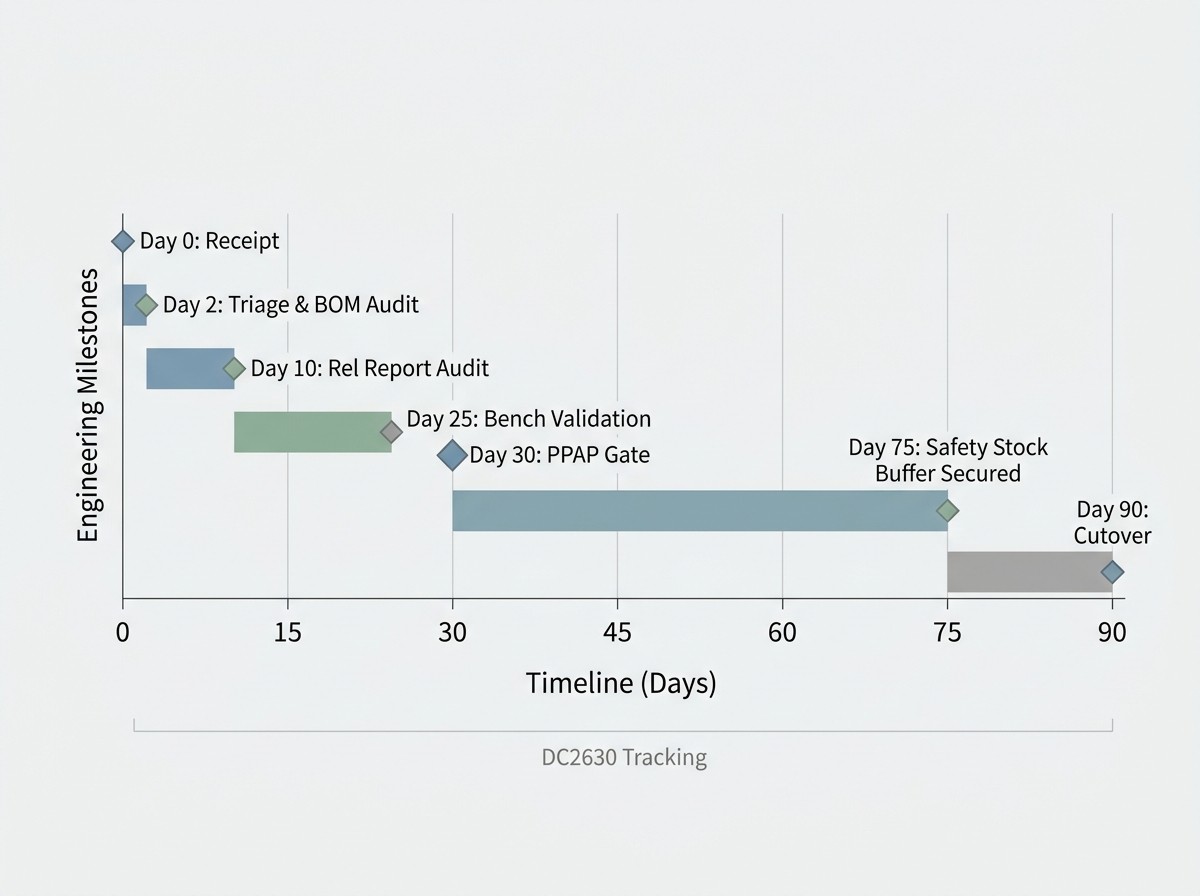
Step 1: Initial Triage and BOM Impact Mapping (Component Engineering)
Upon receipt, the Component Engineer runs the APX32-F407 through the corporate PLM system.
Findings: The part is actively deployed across two designs: an industrial motor inverter and a commercial telemetry gateway. The motor inverter is an industrial mission-critical product with a 10-year operating warranty.
Initial Action: The engineer logs the PCN into the internal change tracking system, records the formal issue date, and sets an alert for the 30-day tacit acceptance deadline. Sourcing is instructed to flag open purchase orders to block the early intake of post-change material.
Step 2: Reliability Report Audit (Supplier Quality Engineering Gate)
The SQE reviews the qualification summary package attached to PCN-2026-EX884. The review checks four critical criteria:
Lot Integrity and Sample Sizes: Under AEC-Q100 and JESD47 qualification standards, stress testing must span three independent manufacturing lots with 77 units per lot (231 units total per test sequence) to account for lot-to-lot process variation. The report confirmssample sizing across all stress sequences.
Acceptance Criteria: Zero failures are allowed (, representing an LTPD of 1% at a 90% confidence level). The data indicates 0 rejects across all legs.
High-Temperature Operating Life (HTOL): Tested per JESD22-A108 for. Static and dynamic leakage currents remain within baseline distribution limits.
Cu-Wire Integrity Verification: The SQE verifies that Biased HAST (, 96 hours) was completed with zero corrosion-induced opens or leakage. The C-SAM acoustic microscopy images are audited, confirming zero delamination along the leadframe and silicon surface. Ball-shear test results confirm sufficient intermetallic bonding without pad cratering beneath the dielectric layers.
Step 3: Hardware Bench Re-Characterization (Hardware Engineering Gate)
The hardware team orders 20 engineering samples of the Fab B / Cu-wire revision. The devices are mounted on test boards to run side-by-side comparative A/B testing against original Fab A / Au-wire control units:
Power-On Reset (POR) Transient Margins: The engineer sweeps thepower-rail slew rate fromtoacross extreme temperatures (). The brownout reset trip thresholds match original silicon within a tightwindow.
High-Speed Signal Integrity: CAN-FD and SPI bus lines are probed with high-bandwidth active oscilloscopes. Output slew rates () show a minor acceleration of. The engineer verifies that setup and hold margins remain fully compliant with system specifications, and ringing does not violate signal integrity boundaries.
Thermal dissipation: An infrared (IR) camera profiles the MCU running at 100% core computational load for two continuous hours. Package surface temperature matches the baseline design within, confirming die-attach thermal resistance () parity.
Step 4: Supply Chain Cutover & Safety Stock Strategy (Procurement Gate)
Because full validation requires 45 days (exceeding the standard 30-day objection window), Procurement issues a formal Interim Technical Hold Letter to Apex Microelectronics on Day 18. This letter freezes the tacit acceptance clock, explicitly stating that approval is contingent on internal bench validation completion.
Simultaneously, Sourcing models factory run-rates and secures a 90-day safety stock buffer of original Fab A / Au-wire inventory. This buffer guarantees continuous production in the event that internal bench testing identifies a subtle defect requiring vendor escalation.
Procurement confirms the supplier’s cutover traceability: the new revision will enter production beginning with date code DC2630.
Step 5: Engineering Sign-Off and Formal Disposition
Following successful bench and software regression testing, the engineering lead issues the formal disposition:
Disposition Decision: CONDITIONAL APPROVAL GRANTED
Reason: Qualification data and internal bench testing meet all requirements.
Condition: Final approval for the industrial motor inverter line is gated on PPAP Level 3 document submission and validation of the first SMT pilot run.
The team executes an internal Engineering Change Order (ECO). Incoming inspection systems are updated to flag date code DC2630, directing the first arriving post-change reels to SMT engineering for solder paste verification and line clearance.
In-House Hardware Lab Bench Validation Protocol
When a semiconductor manufacturer issues a major PCN, internal bench testing should focus on application boundaries that standard IDM qualification testing does not cover.
Integrated circuit manufacturers qualify parts against standard JEDEC/AEC fixtures with clean, lumped loads. Your physical PCB contains distributed trace capacitances, inductive power planes, power supply ripple, and complex firmware state transitions.
Execute this lab validation protocol on incoming engineering samples before signing off on a major change:
1. Power-On Reset (POR) and Power-Supply Slew Verification
Connect a programmable power supply to the device's supply pins. Programramp rates spanning the widest conceivable range (to).
Subject the unit to rapid power cycling (power dips, brownouts, and microsecond dropouts) to confirm the internal power-on reset circuitry cleanly resets the device without causing latch-up, memory corruption, or undefined logic states.
Repeat this verification inside a temperature chamber at your system's operational extremes (e.g.,and).
2. High-Speed Bus Signal Integrity & Edge-Rate Analysis
Use high-bandwidth active differential probes to capture output waveforms on high-speed communication buses (SPI, QSPI, I2C, CAN-FD, USB, or parallel memory interfaces).
Measure rise () and fall () times directly. Check for sharp transitions that inject excessive high-frequency harmonics into surrounding traces.
Inspect waveforms for transmission-line ringing, undershoot, and overshoot. Ensure that input diode clamping voltages are not exceeded. Confirm that timing margins (clock-to-out, data setup, and data hold times) conform to system timing budgets.
3. Thermal Dissipation and Die-Attach Integrity
Flash the sample with firmware configured to exercise all internal computational engines, peripherals, and output drivers simultaneously, driving power consumption to maximum operational limits.
Remove any active heatsink and use a calibrated radiometric infrared (IR) camera to profile the package surface temperature.
Compare the thermal map against an original control component. A localized hot spot indicates localized die-attach voiding, high junction-to-case thermal resistance, or non-uniform current density across the revised die.
4. Dynamic Transient Current () Spikes
Monitor transient supply currents by placing a high-frequency current probe or a low-value series sensing resistor directly in line with the mainrail.
Trigger transitions between low-power sleep states and high-performance active processing modes.
Examine the resulting transient inrush currents. Confirm that your board's existing decoupling capacitor network (bulk and ceramic bypass capacitors) can support these switching transients without allowing the supply rail to sag below the minimum operating voltage threshold.
5. Firmware and Register Boundary Regression
Flash the target device with your production firmware image.
Execute an automated test harness covering all hardware register configurations, interrupt priorities, peripheral handshakes, and communication protocols.
Verify that unadvertised errata fixes or changes to internal hardware state machines do not cause race conditions, unhandled exceptions, or driver lockups in legacy codebase routines.
Frequently Asked Questions (FAQ)
What should we do if the supplier cannot provide physical samples before the 30-day response window closes?
If a supplier cannot supply engineering evaluation samples before their stipulated feedback deadline expires, issue an official, written Technical Hold / Interim Objection Letter.
State explicitly that your organization invokes the evaluation provisions of J-STD-046, that the sample delivery date represents the true starting point of your evaluation period, and that the PCN is placed on formal hold pending receipt, evaluation, and written approval of physical samples.
Copy both the supplier's sales representative and your authorized distributor’s quality team. This freezes the acceptance clock and legally blocks the supplier from citing tacit approval.
How do we handle PCNs issued through catalog distributors where direct IDM access is unavailable?
When purchasing through high-service catalog distributors (such as DigiKey, Mouser, or Farnell), direct access to the component manufacturer’s field quality teams is often restricted. In this scenario:
Submit an immediate support ticket to the distributor's quality assurance team requesting the complete manufacturer qualification report and PCN tracking number.
Use the manufacturer’s public quality portal (e.g., Texas Instruments Quality & Reliability Dashboard or onsemi PCN portal) by searching the exact base part number to locate the original technical notification.
If critical technical validation cannot be resolved and the distributor cannot guarantee traceability by manufacturing date code, implement an internal risk mitigation plan: schedule an incoming inspection gate to segregate new date codes until pilot production validation is complete.
Can an engineering team legitimately reject a PCN if the vendor meets all datasheet parameters?
Yes. Component datasheets capture static parameters under tightly bounded test conditions; they do not encompass the entirety of a system's application profile. Valid grounds for rejection include:
Unacceptable degradation in board-level solderability or SMT thermal process profiles.
Thermal dissipation changes () causing over-temperature conditions in passively cooled enclosures.
Excessive electrical noise, edge-rate acceleration, or parasitic ringing that violates system-level electromagnetic compatibility (EMC/EMI) regulatory filings.
Regulatory recertification triggers (e.g., medical device FDA 510(k) filings, aviation FAA conformity, or functional safety ISO 26262 audits) where unnotified process changes invalidate prior compliance certifications.
When rejecting a PCN, provide the supplier with clear engineering documentation: include failure logs, oscilloscope captures, thermal imaging comparisons, or radiographic/microscopic evidence.
What are the physical risks of mixing pre-change and post-change date codes on the same SMT assembly line?
Mixing old and new revisions within the same production run or across identical feeder reels introduces significant manufacturing and quality control risks:
SMT Profile Incompatibility: If the PCN modified the leadframe plating (e.g., matte tin to nickel-palladium-gold) or package mold compound, the optimal reflow solder profile (wetting speed, peak temperature, cooling rate) may vary. Running mixed parts down the same line leads to cold solder joints, tombstoning, or voiding.
Vision Inspection System False Calls: Subtle variations in package reflectivity, pin-one dimple markings, or laser-etch contrast cause Automated Optical Inspection (AOI) systems to register false part-orientation defects, causing production line stoppages.
Traceability Loss During Containment: If a field failure occurs, mixing date codes across serial numbers makes clean lot-tracing impossible. Instead of isolating and recalling a specific, bounded manufacturing sub-lot, your quality department may be forced to quarantine and recall an entire production block, multiplying warranty exposure.
Sources and references used for this guide
J-STD-046A: Customer Notification Standard for Product/Process Changes by Electronic Product Suppliers
Source type: standards body
Used for: Industry standard definition for product change notifications, major change thresholds, and 90-day notification guidelines.
Caution: Voluntary consensus industry standard; specific customer contracts or master purchase agreements can supersede standard timelines.JESD46C: Customer Notification of Product/Process Changes by Solid-State Suppliers
Source type: standards body
Used for: Historical foundational standard for semiconductor product/process change notification requirements.
Caution: Largely superseded by joint standard J-STD-046 across general electronic component manufacturing.JESD47: Stress-Test-Driven Qualification of Integrated Circuits
Source type: standards body
Used for: Baseline reliability stress test specifications (HTOL, HAST, TC) and requalification guidelines for IC modifications.
Caution: Defines commercial/industrial baseline; automotive applications require more stringent AEC-Q100 qualification standards.Texas Instruments Product Change Notification (PCN) Policies & Guidelines
Source type: official company documentation
Used for: Real-world Tier-1 IDM implementation of J-STD-046 compliance, 90-day customer notification rules, sample availability, and tracking procedures.
Caution: Vendor documentation; illustrates standard supplier practices, but proprietary notification portal details apply specifically to Texas Instruments.Texas Instruments General Quality Guidelines (Rev. Q)
Source type: official company documentation
Used for: Component qualification baselines, date code traceability, fab/assembly change notification protocols, and quality control systems.
Caution: Supplier quality manual; represents IDM operational requirements and standard terms.NXP Change Management and Customer Communication Policy
Source type: official company documentation
Used for: Substantiating the 30-day customer objection window, tacit approval terms of sale, and application of DeQuMa in packaging/fab changes.
Caution: Manufacturer terms of sale; highlights the commercial reality of supplier default approval timelines.NXP Copper Wire Qualification Delta Qualification Matrix (PCN 16663 / 16793)
Source type: official company documentation
Used for: Authentic example of a semiconductor manufacturer applying the ZVEI DeQuMa framework to qualify gold-to-copper wire bonding transitions.
Caution: Device-specific qualification report attachment; serves as a technical structural reference rather than universal test data.Infineon Technologies Product Change Notification Quality Guidelines
Source type: official company documentation
Used for: Corroboration of the 90-day minimum advance notice and 30-day customer feedback period under J-STD-046.
Caution: Vendor documentation; confirms broad consensus across European IDMs regarding change notification response windows.
 UTMEL
UTMEL
We are the professional distributor of electronic components, providing a large variety of products to save you a lot of time, effort, and cost with our efficient self-customized service. careful order preparation fast delivery service
 Modeling Wide Band-Gap Semiconductors for Enhanced PerformanceRakesh Kumar, Ph.D.31 January 20243778
The article delves into the challenges faced by silicon-based power electronic devices and highlights the potential of wide band-gap semiconductors. It also emphasizes the importance of modeling power semiconductor devices and provides insights into various models. For electrical energy conversion to be dependable and effective, power electronics and semiconductor device technologies are essential.
Read More Optimizing Energy Management with Non-Isolated DC-DC ConvertersRakesh Kumar, Ph.D.04 February 20243421
The article classifies DC-DC converters and discusses the benefits and limitations of them. It proposes a modified DC-DC converter topology that combines the Cuk and Positive Output Super Lift Luo topologies to achieve a higher voltage gain with fewer components.
Read More ‘6G Networks’ - Pioneering the Next Era of Connectivity And InnovationRakesh Kumar, Ph.D.18 March 20243741
The article provides a comprehensive overview of the evolving landscape of mobile networks, the requirements that will shape the future of mobile communication, and the innovative technologies driving the transition to 6G.
Read More Review of IoT-Based Smart Home Security Systems- Part 1Rakesh Kumar, Ph.D.28 March 20244218
The article discusses the evolution of IoT-based smart home security systems, integrating advanced technologies like Raspberry Pi, PIR sensors, and voice recognition for enhanced user experience and efficiency.
Read More Understanding Photodiodes: Working Principles and Applications - Part 2Rakesh Kumar, Ph.D.24 May 20245425
The article provides a comprehensive overview of photodiodes, focusing on their operational principles, key factors affecting their efficiency, advantages, and disadvantages, and highlights their diverse applications.
Read More
Subscribe to Utmel !
![2020-204/000-038]() 2020-204/000-038
2020-204/000-038WAGO
![272-133/101-000]() 272-133/101-000
272-133/101-000WAGO
![MAX6519UKP075]() MAX6519UKP075
MAX6519UKP075Analog Devices
![T30UDPA-CRFV]() T30UDPA-CRFV
T30UDPA-CRFVBanner Engineering
![T30UHPBQ]() T30UHPBQ
T30UHPBQBanner Engineering
![620005N003]() 620005N003
620005N003TE Connectivity
![MAX6517UKP005 T]() MAX6517UKP005 T
MAX6517UKP005 TAnalog Devices
![832AD]() 832AD
832ADErsa
![39.5451]() 39.5451
39.5451Altech
![EB41D2424]() EB41D2424
EB41D2424Desco