

 Product
 Brand
Brand Articles
 Tools
Tools
MLCC DC Bias Derating: How to Calculate and Compare Effective Capacitance Before Component Selection
Evaluating multilayer ceramic capacitor (MLCC) DC bias derating is an essential pre-procurement qualification step for power supply designers, hardware engineers, and component selection teams. Nominal capacitance ratings printed on manufacturer datasheets reflect standardized zero-bias laboratory test conditions (,,) specified under IEC 60384-9 and EIA RS-198. When energized on active DC voltage rails, Class II ferroelectric MLCCs (such as X5R, X7R, and X8R) suffer severe capacitance degradation—often exceeding 50%–80% loss in compact footprints[1]. Consequently, relying on nominal ratings without calculating true in-circuit effective capacitance () leads to control loop instability, degraded transient response, and premature power supply failure.
The Solid-State Physics of DC Bias Derating: Why Datasheets Mislead
Class II MLCC capacitance drops under DC bias because of ferroelectric domain saturation[2] within the ceramic lattice. Under an external electric field, spontaneous electric dipoles align and lock along field lines, reducing the dielectric material's relative permittivity and effective capacitance.

Ferroelectric Dipole Saturation in Barium Titanate () Dielectrics
Class II MLCCs utilize barium titanate () as their primary dielectric base. Below its Curie transition temperature (),shifts from an isotropic cubic crystal structure into an anisotropic tetragonal lattice. This non-centrosymmetric state creates spontaneous polarization domains.
At zero DC bias, these ferroelectric domains are oriented in random directions. When a small-signal AC voltage is applied, the domain walls oscillate freely, yielding high relative permittivity () and high volumetric capacitance.
However, applying an external DC voltage establishes an internal electric field that forces spontaneous dipoles to rotate and align parallel to the field. As the applied voltage rises, more domains reach full saturation. Because these locked dipoles can no longer respond dynamically to superimposed AC excitation, relative permittivity drops sharply, reducing in-circuit capacitance.
Standard Zero-Bias Test Conditions (EIA RS-198 / IEC 60384-9)
Datasheet ratings reflect industry testing baselines rather than operating conditions. Under IEC 60384-9 (Class 2 Fixed Ceramic Capacitors) and EIA RS-198-1-F, factory incoming and outgoing inspection measurements require:
DC Bias: Exactly
Ambient Temperature:
AC Excitation:at(for capacitors, drive voltage frequently drops toor lower to prevent self-heating)
Consequently, a component that passes incoming inspection at 100% nominal value on a passive LCR bridge can drop by more than half its capacitance once soldered into an active 3.3V, 5.0V, or 12.0V power rail.
Class I (C0G/NP0) vs. Class II (X5R/X7R/X8R) Dielectric Behavior
The voltage coefficient of capacitance (VCC) depends directly on the crystalline chemistry of the dielectric:
Class I Ceramics (C0G / NP0): Formed from non-ferroelectric, paraelectric titanates (e.g., neodymium or samarium titanates). Because they possess no spontaneous domain structure, Class I capacitors exhibit $0\%$ DC bias derating across their entire operating voltage range. However, their modest relative permittivity () limits their volumetric efficiency, making them practical primarily for high-frequency RF filtering, precision timing, and snubber circuits below.
Class II Ceramics (X5R, X7R, X8R): Formed from doped. They deliver orders-of-magnitude higher volumetric capacitance within sub-millimeter packages. The engineering trade-off is non-linear voltage, temperature, and time-dependent aging characteristics.
Package Geometry, Voltage Rating, and Electric Field Intensity ()
DC bias derating in Class II ceramics is governed by the internal electric field strength (), not by operating voltage alone. Package miniaturization thins dielectric layers, driving up field intensity and causing compact packages to derate significantly faster than larger case sizes[5] at identical voltages.
The Governing Role of Dielectric Layer Thickness ()
The internal electric field gradient across each active ceramic layer is expressed as:
Where:
is the electric field intensity ()
is the operational DC bias voltage (V)
is the individual dielectric layer thickness ()
To pack high capacitance into miniature footprints (e.g.,in an 0402 or 0603 footprint), manufacturers reduce the dielectric layer thickness down to sub-micron levels () and stack hundreds of active layers. Whenis applied across an 0402 capacitor with adielectric layer, the internal field reaches, pushing theceramic deep into dipole saturation.
Conversely, an equivalentcapacitor in a larger 1206 footprint uses thicker dielectric barriers (). At the samebias, the internal field remains below, preserving a substantially higher percentage of its nominal capacitance.
Why the "2x Rated Voltage" Rule Fails in Downsized Packages
A common design heuristic suggests that selecting an MLCC with a voltage rating twice the operating rail (e.g., using aorrated capacitor on aline) avoids significant DC bias loss. In compact Class II ceramics, this rule is unreliable.
For example, a high-density,0603 X5R MLCC operating atbias retains approximately 40% of its nominal capacitance[3] (a $60\%$ loss). In contrast, an equivalent,1206 X7R MLCC at that samebias retains approximately $80\%$ of its nominal rating.
Increasing rated voltage within an identical miniature case size (e.g., choosing a0402 over a0402) often requires the manufacturer to use fewer total layers, meaning the dielectric layer thickness () cannot scale up proportionally without sacrificing capacitance. Stepping up physical case size remains far more effective for preserving in-circuit capacitance than increasing rated voltage within an ultra-small package.
The Geometric Trade-off: Footprint Real Estate vs. Retained Capacitance
Downsizing MLCCs to save PCB area frequently backfires at the system level. If an 0402capacitor loses $80\%$ of its value under abias, it yields an effective capacitance of only. The design then requires five 0402 capacitors in parallel to achieve a targeteffective pool.
Those five 0402 components—along with their solder lands, routing traces, and manufacturing clearances—consume more routing channels and total board surface area than a single 0805 or 1206 capacitor that retainsunder the same bias.
Multi-Vendor Simulation and Extraction: Comparing Parts Before Purchasing
Cross-referencing MLCCs across suppliers requires comparing vendor-specific simulation models at the intended operating voltage and temperature. Manufacturers use proprietary dopants and grain structures that cause identical nominal ratings to deliver divergent effective capacitance.
Navigating Tier-1 Manufacturer Design Platforms
Leading ceramic capacitor manufacturers maintain dynamic simulation portals that model non-linear DC bias, temperature, AC drive, and frequency behavior:
Murata SimSurfing: Allows dynamic sweeping of DC voltage, ambient temperature, AC ripple voltage, and S-parameters. Provides combined $C-V-T$ derating models and downloadable SPICE netlists.
TDK Component Characteristics Viewer (CCV) & SEAT: Displays dynamic DC superimposition curves, complex impedance sweeps, and loss tangent data across bias and temperature profiles using dynamic DC bias simulation models[4].
Samsung Electro-Mechanics EMCompass: Features multi-part comparative overlays, thermal derating modeling, and power loss calculations.
KEMET K-SIM: Provides real-time calculations of in-circuit capacitance, ripple current thermal rise, and transient behavior under user-defined rail voltages.
Secondary Operating Variables: AC Ripple Amplitude () Superimposition
Measured capacitance in Class II dielectrics is non-linear and depends on the amplitude of superimposed AC ripple voltage. When an MLCC experiences low-frequency AC ripple from a switching regulator, higher AC ripple excitation () provides sufficient field energy to force partial domain movement, temporarily increasing measurable capacitance.
Conversely, when the AC ripple amplitude is small (e.g.,on a clean, quiet LDO output), the dielectric remains locked by the DC field, and capacitance matches the lower boundary of the DC bias curve. Hardware engineers must verify that simulation parameters match the actual AC ripple amplitude of the circuit.
Cross-Referencing Alternative Sources: Why Equivalent Part Numbers Diverge
Procurement and component engineers frequently treat MLCCs with matching nominal ratings (,, X7R,) as interchangeable drop-in equivalents across manufacturers. However, physical architectures vary widely between vendors:
Barium Titanate Grain Size: Fine-grain ceramics () yield higher initial permittivity but drop faster under moderate electric fields. Coarser grain formulations preserve better linearity at the expense of baseline volumetric efficiency.
Rare-Earth Dopants: Proprietary additives (such as dysprosium, holmium, or yttrium oxides) shift the Curie peak and modify domain pinning dynamics.
Internal Layer Counts: One vendor may achieveusing 300 ultra-thin layers, whereas another uses 220 slightly thicker layers, leading to differentgradients.
Consequently, benchmarking data shows that equivalent nominal parts from different Tier-1 suppliers can show adivergence in retained capacitance at operating voltage. Drop-in approvals must be qualified against effective capacitance curves rather than nominal datasheet ratings.
Effective Capacitance Comparison Matrix (Class II MLCCs)
The following matrix illustrates typical retained capacitance values across different package footprints and DC bias operating points atwithAC excitation:
| Case Size (EIA) | Nominal Rating | Rated Voltage () | Dielectric Code | Retainedat | Retainedat | Retainedat | Retainedat |
|---|---|---|---|---|---|---|---|
| 0402 (1005 Metric) | X5R | Exceeds | |||||
| 0603 (1608 Metric) | X7R | Exceeds | |||||
| 0603 (1608 Metric) | X7R | ||||||
| 0805 (2012 Metric) | X7R | ||||||
| 1206 (3216 Metric) | X7R |
Note: Data represents industry-standard characterization averages extracted from vendor tools (Murata SimSurfing, TDK CCV). Exact curves depend on internal layer geometry and dopant chemistry.
The Multi-Factor Worst-Case Derating Formula
Calculating true minimum in-circuit capacitance requires compounding nominal manufacturing tolerance, temperature-induced variation, DC bias loss, and long-term logarithmic dielectric aging into a unified equation.
The Unified Effective Capacitance Equation
To verify that a power supply or decoupling network meets its operational baseline across all operating conditions, calculate worst-case effective capacitance () using:
Where:
: Nominal catalog capacitance (,)
: Initial manufacturing tolerance (,)
: Maximum temperature coefficient of capacitance loss over operating range (e.g.,for X7R fromto)
: Fractional capacitance loss extracted from manufacturer curves at operating DC rail voltage
: Fractional logarithmic aging loss over operating lifetime
When dynamic web simulation tools provide coupled DC bias plus temperature curves (), simplify the formulation to:

Class II Dielectric Logarithmic Aging and Reflow De-Aging Dynamics
Class II ceramic dielectrics undergo spontaneous domain stabilization over time. As the crystal structure relaxes, relative permittivity decays predictably on a logarithmic timescale[8] according to:
Where:
is the aging rate (% loss per decade hour)
is the referee time baseline (standardized atby EIA-198)
is the elapsed operating time in hours post-Curie transition
Typical decade-hour aging rates () are:
X7R Dielectrics:per decade hour
X5R Dielectrics:per decade hour
C0G / NP0 Dielectrics:(No measurable aging)
The De-Aging Mechanism: When an MLCC is heated above its Curie transition point () during standard SMT reflow soldering (peak profiles), the tetragonally distorted lattice returns to a cubic state. This resets the aging clock to.
Upon cooling below the Curie point, the component measures above its nominal rating and begins a new logarithmic aging cycle. After 10,000 operational hours (decade 4 from 1 hour), an X7R capacitor loses roughlyfrom its initial post-reflow capacitance.
Coupling Temperature Variation with DC Bias
Temperature and DC bias effects do not superimpose purely linearly. When an external DC bias is applied to an MLCC, the internal electric field partially suppresses the Curie peak, which flattens the temperature coefficient curve across its operating thermal range.
At high temperatures (), increased thermal lattice vibrations can disrupt domain locking, sometimes yielding a slight increase in effective capacitance relative to its room-temperature biased state. High-reliability calculations should evaluate the combined $C(V, T)$ data directly via vendor simulation tools rather than treating temperature and bias as isolated variables.
System-Level Circuit Impacts: Power Integrity, Loop Stability, and Resonant Shifts
Unmodeled DC bias derating alters the small-signal dynamics of switching converters, shifting feedback control poles, reducing loop phase margins, and raising the capacitor's self-resonant frequency.

DC-DC Converter Control Loop Pole Migration and Phase Margin Erosion
In voltage-mode switching regulators, the output LC filter forms a double pole that sets loop roll-off:
In peak current-mode buck converters, the power stage response is governed by a load-dependent dominant pole:
When Class II output capacitors loseof their capacitance under operating rail bias, the output pole shifts to a higher frequency. This migration pushes the loop unity-gain crossover frequency () higher, reducing phase margin.
If the phase margin drops below 45 degrees[6], the regulator's transient response becomes underdamped, showing excessive voltage ringing and settling overshoot during load steps. Severe derating can cause phase margin to drop below, triggering sustained control loop oscillation and power rail collapse.
Upward Shift in Self-Resonant Frequency (SRF)
The self-resonant frequency () of an MLCC marks the boundary between its capacitive and inductive impedance characteristics:
While equivalent series inductance () is fixed by package geometry and board mounting loops, effective capacitance () decreases under DC bias. As a result, the impedance resonance notch shifts higher in frequency.
In benchtop impedance characterization of a,0603 X5R MLCC (e.g., Murata GRM188R61C105MA12) across bias sweeps:
AtBias: Measureswith an SRF of.
AtBias: Capacitance drops to, shifting SRF to.
AtBias: Capacitance drops to(a $52\%$ loss), shifting the SRF notch up to.
This resonance shift alters the capacitor's high-frequency decoupling profile, degrading impedance at frequencies where low PDN impedance was originally targeted.
Dynamic Voltage Ripple and Piezoelectric Microphonics
Output voltage ripple in a standard buck converter[7] is inversely proportional to effective output capacitance:
A capacitor bank whose effective value derates by $75\%$ produces a four-fold increase in output voltage switching ripple, potentially exceeding the ripple tolerance of sensitive FPGAs, ASICs, or RF transceivers.
Additionally, because barium titanate is ferroelectric, it exhibits strong electrostrictive and piezoelectric properties. When AC ripple voltage is superimposed on high DC bias fields, the ceramic undergoes mechanical deformation at the converter switching frequency.
If this switching frequency or its subharmonics fall within the human audible range (), the capacitor flexes against the PCB substrate, generating acoustic noise ("singing capacitors") and inducing microphonic voltage spikes on adjacent high-impedance analog sensor traces.
Benchtop Laboratory Verification: Measuring Effective Capacitance Under DC Bias
When characterizing unmodeled or second-source MLCCs, hardware design teams can measure effective capacitance using precision LCR meters or 2-port shunt-thru vector network analyzers (VNAs) equipped with external DC bias fixtures.
Ceramic Capacitor DC Bias Effects & Measurement - Phil's Lab #152
4-Terminal-Pair LCR Meter Configuration
High-precision sweeps at lower frequencies () use a 4-terminal-pair LCR meter (e.g., Keysight E4980A/AL) combined with an external DC bias adapter (such as the Keysight 16065A/C, rated up to):
Port Isolation: The external fixture uses internal DC blocking capacitors (typicallyhigh-voltage film types) to isolate the LCR meter's current and voltage sensing bridges from the external DC power supply.
Excitation Guarding: Set the AC drive level to a standard baseline (or). Perform open-circuit and short-circuit fixture compensation with the DC bias supply connected and powered (set to) to null out fixture parasitics and stray terminal capacitance.
2-Port Shunt-Thru VNA Impedance Architecture
For broadband power integrity and PDN impedance characterization (), engineers use a 2-port shunt-thru impedance setup with a vector network analyzer (e.g., Omicron Lab Bode 100):
Signal Path: The VNA source connects through a custom DC-block and bias-injection module to the device under test (DUT). The transmission response passes through a second DC-blocking network, through a low-frequency common-mode choke (e.g., Omicron B-LCM) to break ground loops, and into the VNA receiver channel.
Bias Injector Construction: The DC injection network uses a bias resistor () tied to a low-noise programmable DC power supply. The DC blocking capacitor () must provide a large capacitance—such as a bank of forty (40)capacitors in parallel—to push the fixture's high-pass cut-off frequency well belowto prevent measurement distortion at low frequencies.
RF Drive Management: Set the VNA RF source power low (e.g.,) with appropriate receiver attenuation. Driving MLCCs with excessive AC signal amplitudes triggers non-linear dielectric distortions that mask pure DC bias behavior.
Measurement Hazards: TransientSpikes and Fixture Derating
Operating high-voltage DC bias fixtures requires specific precautions to protect sensitive instrumentation:
TheInput Damage Hazard: Vector network analyzer receiver inputs (typicallyterminated) are rated for low maximum damage thresholds, often around(maximum input). When changing DC bias voltages during sweeps, never step the power supply voltage rapidly. Fast voltage transitions create highcurrent spikes that pass directly through the series blocking capacitors, risking severe overload to the VNA receiver frontend. Program power supply slewing rates to gentle ramp profiles ().
Fixture Capacitor Self-Derating: If the series blocking capacitors () inside the test fixture are themselves Class II ceramic MLCCs, the injected DC bias voltage will derate the test fixture's own internal capacitance. This dynamic shift alters the fixture's low-pass filter corner during testing. For accurate low-frequency characterization, construct test fixture blocking banks using Class I C0G ceramics, high-voltage film capacitors, or re-calibrate the baseline across every discrete DC bias voltage step.
What the Engineering Community Reports
Hardware engineers across technical forums frequently discuss practical challenges when managing MLCC DC bias derating in production:
Unannounced Alternative Sources: Component engineers often note that alternative parts approved during supply crunches cause field issues. Even when secondary vendors match nominal datasheet ratings, different internal layer counts can result in steeper DC bias curves, occasionally causing regulator instability or transient ripple failures.
Incomplete Vendor Datasheets: Hardware teams often encounter commodity MLCC datasheets that lack detailed DC bias curves, providing only room-temperature zero-bias ratings. In these cases, engineers typically rely on benchtop LCR measurements or conservative derating assumptions before approving unmodeled parts.
Acoustic Noise from Ceramic Vibration: Designers frequently report microphonic board noise in automotive and consumer audio devices. When Class II ceramics on high-voltage rails experience AC switching currents, mechanical deformation generates audible whistling, requiring layout changes or substitutions with low-acoustic Class I or metal-composite inductors.
Pre-Procurement Engineering Checklist
To verify Class II ceramic capacitors across all operational envelopes, apply the following pre-procurement audit before finalizing schematics, releasing bills of materials (BOM), or approving vendor second sources:
Audit In-Circuit Operating Voltage:
Identify all Class II MLCCs on active DC rails (,,,,,).
Note the actual operating DC voltage across each part.
Extract Manufacturer DC Bias Curves:
Query the specific vendor part number in official simulation tools (Murata SimSurfing, TDK CCV, Samsung EMCompass, KEMET K-SIM).
Record the exact fractional loss () at operating rail voltage and operating AC ripple amplitude.
Compound Competing Degradation Factors:
Subtract initial tolerance (, typically $-10\%$ or $-20\%$).
Subtract worst-case temperature coefficient derating over operating temperature (e.g., $-15\%$ for X7R overto).
Subtract end-of-life logarithmic aging loss ().
Evaluate Package Downsizing Trade-offs:
If using 0402 or 0603 footprints on rails, verify whether stepping up to an 0805 or 1206 footprint provides higher retained capacitance than paralleling multiple miniature parts.
Verify Control Loop and Filter Stability:
Input calculated worst-case effective capacitance () into DC-DC converter stability models.
Verify that loop phase margin remainsacross all line and load conditions, and confirm that peak-to-peak output voltage ripple () remains within downstream component specifications.
Frequently Asked Questions
Why don't MLCC manufacturers list effective capacitance under DC bias on the first page of the datasheet?
International manufacturing standards (IEC 60384-9 and EIA RS-198) require zero-bias test conditions (,,) to establish a uniform, repeatable baseline for factory binning and quality assurance. Because DC bias derating varies non-linearly with operating voltage, AC ripple amplitude, and temperature, manufacturers provide dynamic web-based simulation models and characteristic curve datasets rather than a single fixed datasheet value.
Does selecting a higher rated voltage (e.g., 25V instead of 10V) always guarantee higher effective capacitance?
Not necessarily. In miniature packages (such as 0201, 0402, and high-capacitance 0603s), increasing voltage rating often forces manufacturers to use fewer active internal layers to maintain internal standoff margins. Consequently, the dielectric layer thickness () may not increase enough to reduce internal electric field intensity (). Stepping up physical case size (e.g., from 0402 to 0805) is generally more effective for preserving in-circuit capacitance than merely increasing voltage rating within an ultra-compact footprint.
How does SMT reflow soldering affect MLCC aging, and how long does de-aging last?
Exposing Class II MLCCs to SMT reflow temperatures () heats the barium titanate ceramic well above its Curie transition point (). This returns the crystal lattice to an unpolarized cubic structure, resetting the aging clock to. After cooling, the capacitor measures above its nominal value and resumes logarithmic decay (per decade-hour for X7R). Capacitance typically stabilizes near nominal within 24 to 48 hours post-assembly.
Why does small-signal AC drive voltage amplitude change measured DC bias capacitance?
Barium titanate dielectrics exhibit non-linear field sensitivity. When higher AC ripple voltages () are superimposed on top of a static DC bias, the AC field provides sufficient energy to momentarily overcome domain locking, yielding higher measured capacitance. Under quiet DC bias conditions with small AC ripple (), domain walls remain locked, and effective capacitance settles at its lower boundary.
Is it better to use a single large MLCC or multiple parallel smaller MLCCs?
Paralleling multiple smaller MLCCs distributes thermal dissipation and lowers total Equivalent Series Inductance () and Equivalent Series Resistance (). However, if ultra-compact footprints (e.g., 0402) are used, each individual capacitor will suffer steeper DC bias derating due to high internal electric fields (). Paralleling multiple miniature parts can consume more total board area than a single larger capacitor (e.g., 0805 or 1206) that retains a higher percentage of its nominal capacitance. Total effective capacitance must be calculated for both configurations.
References
The voltage characteristics of electrostatic capacitance — Murata Manufacturing Co., Ltd.
Does the capacitance change when a DC voltage is applied to ceramic capacitors? (Capacitors FAQ) — Murata Manufacturing Co., Ltd.
Replacing Electrolytic Capacitor with MLCC, Revised Guide — TDK Corporation
Dynamic DC Bias Model for accurate circuit simulation — TDK Electronics AG
AN-1099: Capacitor Selection Guidelines for Analog Devices, Inc., LDOs — Analog Devices, Inc.
Optimizing the TPS62097 Output Filter — Texas Instruments Incorporated
How to select input capacitors for a buck converter — Texas Instruments Incorporated
Capacitance Ageing of Ceramic Capacitors (Application Note AN0006) — Knowles Precision Devices
 UTMEL
UTMEL
We are the professional distributor of electronic components, providing a large variety of products to save you a lot of time, effort, and cost with our efficient self-customized service. careful order preparation fast delivery service
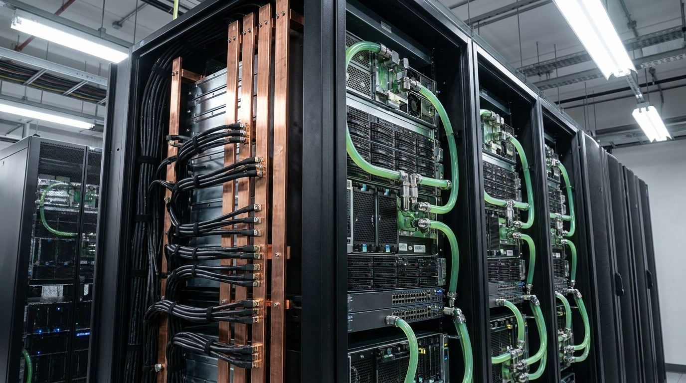 AI Server MLCCs: Why NVIDIA Rubin Racks Require Over 600,000 CapacitorsUTMEL02 June 20263754
Next-generation AI servers like NVIDIA's Rubin architecture require over 600,000 MLCCs per rack due to extreme power densities exceeding 120kW. This transition from GB300 demands high-capacitance, low-ESR capacitors with X7R/X7S dielectrics to handle intense transient responses and thermal loads, forcing procurement teams to navigate extended 24-week lead times for these specialized components.
Read More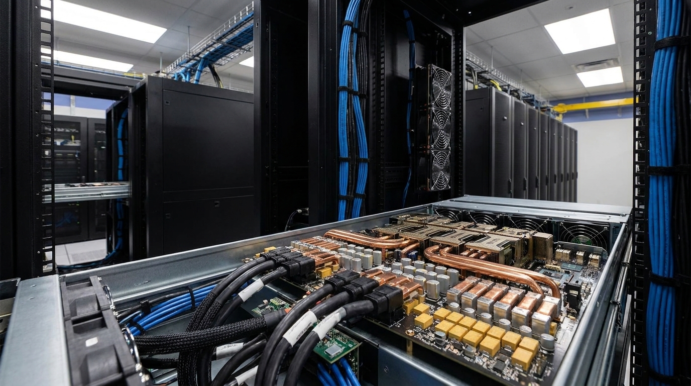 MLCC vs Polymer Tantalum Capacitors: Overcoming 2026 Shortages in AI Server PDNsUTMEL07 August 2026875
Facing 2026 MLCC lead times of up to 24 weeks driven by AI server demand, hardware engineers are substituting multi-layer ceramic capacitors with conductive polymer tantalum capacitors. While Class II MLCCs suffer severe DC bias capacitance loss and acoustic noise, polymer tantalums offer voltage stability and low ESR. Implementing a division-of-labor strategy—using polymer tantalums for bulk decoupling and MLCCs for point-of-load—optimizes PDN performance and bypasses supply bottlenecks.
Read More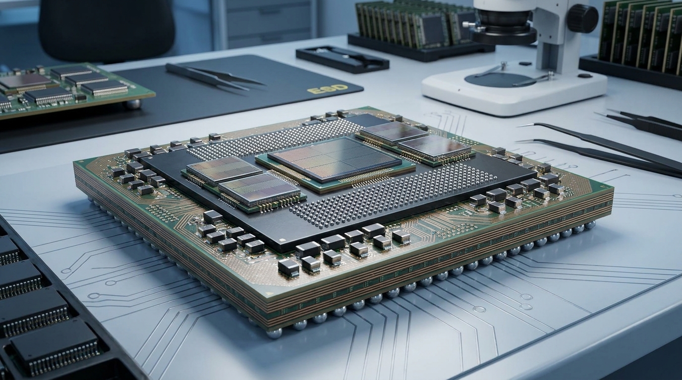 Sourcing Silicon Capacitors and MLCCs in the AI Hardware EraUTMEL13 August 2026728
Modern AI hardware requires a hybrid Power Delivery Network (PDN) to maintain low-voltage stability under extreme transient currents. Deep Trench Silicon Capacitors (DTCs) integrate directly into advanced packages to deliver ultra-low ESL and stable performance for high-frequency transient suppression. Meanwhile, Multilayer Ceramic Capacitors (MLCCs) provide essential bulk energy storage on the motherboard, making both technologies complementary across the AI power stack.
Read More MLCC DC Bias Derating: How to Calculate and Compare Effective Capacitance Before Component SelectionUTMEL11 September 2026841
Class II ceramic capacitors suffer significant capacitance loss under DC voltage due to ferroelectric domain saturation and high electric field intensity. This comprehensive engineering guide explains how to calculate true worst-case effective capacitance by compounding DC bias, temperature, tolerance, and aging. It provides multi-vendor simulation workflows, benchtop impedance measurement techniques, and practical guidelines to maintain power supply stability and avoid costly design failures.
Read More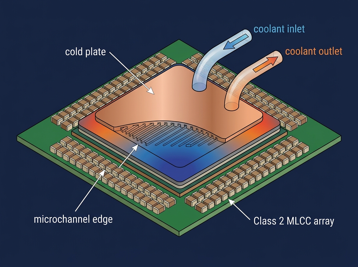 Thermal Management in AI Servers: Specifying Class 2 MLCCs (X7R/X7S) for Liquid Cooling EnvironmentsUTMEL13 July 2026492
Explore how the transition from traditional air-cooling to liquid cooling (direct-to-chip and immersion) in high-density AI server racks alters component thermal profiles. Focus on why design engineers are increasingly specifying Class 2 MLCCs (X7R and X7S dielectrics) over standard X5R variants to prevent thermal degradation near the liquid cooling microchannels. Explain how these capacitors mitigate acoustic noise and voltage bias degradation under heavy workloads. Provide sourcing advice for high-reliability passives via UTMEL during this high-demand memory and passive component super-cycle.
Read More
Subscribe to Utmel !
![RPMH15-1.5-EVM-1]() RPMH15-1.5-EVM-1
RPMH15-1.5-EVM-1RECOM Power
![EF-DI-COMPRESS-SITE]() EF-DI-COMPRESS-SITE
EF-DI-COMPRESS-SITEXilinx
![SI32295AUB20SL0KIT]() SI32295AUB20SL0KIT
SI32295AUB20SL0KITSkyworks
![GAMMA-E3-US]() GAMMA-E3-US
GAMMA-E3-USLattice Semiconductor
![MAX15157BEVKIT#]() MAX15157BEVKIT#
MAX15157BEVKIT#Maxim
![WSA1YR500N-DIGI]() WSA1YR500N-DIGI
WSA1YR500N-DIGISchneider
![V2-EVAL (JP)]() V2-EVAL (JP)
V2-EVAL (JP)FTDI
![M37273E8SS]() M37273E8SS
M37273E8SSRenesas
![M37273ERSS]() M37273ERSS
M37273ERSSRenesas
![A1225A-2PQG100I]() A1225A-2PQG100I
A1225A-2PQG100IMicrosemi Actel
