

 Product
 Brand
Brand Articles
 Tools
Tools
Neuromorphic Chips in AI: Silicon Architecture, Spiking Neural Networks, and Hardware Performance
Contemporary deep learning accelerators spend up to 90% of their total energy budget shuttling dense matrix weights across physical buses between separate memory and compute units rather than performing arithmetic. Neuromorphic chips depart from this synchronous von Neumann paradigm by co-locating memory and processing inside event-driven, brain-inspired silicon. By operating via asynchronous Spiking Neural Networks (SNNs) and in-memory computing, these processors achieve 10× to 100× higher energy efficiency and sub-millisecond response latencies for sparse, streaming temporal data compared to conventional graphics processing units (GPUs).
This guide analyzes the silicon-level mechanics of neuromorphic hardware, the physics of in-memory crossbar arrays, the mathematical methods used to train non-differentiable spiking models, benchmarked hardware profiles across digital and analog architectures, and the engineering trade-offs governing edge deployments versus datacenter Large Language Models (LLMs).
The Hardware Crisis: The Von Neumann Bottleneck and the Limits of Synchronous AI
Traditional computing architectures separate central processing units from memory via physical communication buses, creating a throughput and energy ceiling known as the von Neumann bottleneck.
In standard synchronous systems, arithmetic logic units repeatedly query off-chip storage across high-energy buses, cycling constantly under a global clock. In contrast, non-von Neumann neuromorphic architectures integrate synaptic storage directly beside neuron arithmetic circuits, operating completely asynchronously without a global clock and dissipating negligible dynamic power when idle.
The Physics of the Memory Wall
In standard synchronous architectures, computing a single multiply-accumulate (MAC) operation requires fetching operands from memory registers, executing the arithmetic logic, and writing results back to storage. According to foundational energy benchmarks presented by Mark Horowitz at IEEE ISSCC, reading a 32-bit word from off-chip dynamic random-access memory (DRAM) consumes between 1.3 nJ and 2.5 nJ (1,300 to 2,500 pJ) of energy. In contrast, executing a 32-bit floating-point MAC operation directly on silicon consumes approximately 0.9 to 3.7 pJ.
Consequently, data movement across the physical bus consumes between 200× and 1,000× more energy than the actual mathematical computation. As deep neural networks scale to hundreds of billions of parameters, this architectural separation causes memory bandwidth saturation, severe thermal throttling, and unsustainable power consumption at sub-3nm lithography nodes.
Conversely, the biological human brain operates on an estimated power envelope of approximately 20 W while supporting roughly 86 billion neurons andtosynaptic interconnections. Biological systems achieve this efficiency because synapses serve simultaneously as the computational elements and the persistent storage substrate, eliminating data transit between disparate memory and logic units.
Continuous Clock Cycles vs. Event-Driven Asynchrony
Conventional GPUs and tensor processing units (TPUs) rely on high-frequency global clock signals (typically 1.5 to 2.5 GHz) to synchronize millions of arithmetic logic units (ALUs). These processors continuously execute cycles across dense matrix tensors regardless of whether the underlying input data has changed, resulting in high static power dissipation.
In visual stress tests and architectural cross-sections, researchers observe that neuromorphic silicon operates without a global synchronization clock. Rather than continuous cycles, data pipelines remain quiescent until triggered by discrete information bursts. Transistors draw active switching current exclusively when an incoming voltage spike arrives at a neuron circuit. In the absence of incoming temporal events, the dynamic power dissipation drops to near zero.
Dense Matrix Multiplication vs. Sparse Temporal Processing
Modern deep learning frameworks cast machine learning workloads into dense matrix-matrix multiplications (GEMM) running on parallel Single Instruction, Multiple Threads (SIMT) architectures. While SIMT excels at uniform, batch-processed workloads like training autoregressive transformers, it exhibits structural inefficiencies when handling real-time, sparse, temporal data streams:
Sparsity Handling: In sparse edge workloads (such as vibrational telemetry or continuous biosignals), over 95% of sensor values remain unchanged between samples. A GPU processes these zero-value tensors through its standard execution pipelines, wasting floating-point capacity.
Temporal Granularity: GPUs achieve high compute density by buffering input streams into batches, introducing latency penalties (10 to 50 ms) incompatible with high-speed closed-loop control.
Power Scaling: Under low-workload streaming conditions, a high-performance GPU retains high idle power draw (often 30 to 70 W base idle), whereas an event-driven processor scales power consumption proportionally with incoming event frequency.
Neuromorphic Architecture: Silicon Neurons, Synapses, and In-Memory Physics
Neuromorphic engineering replaces von Neumann abstraction layers with physical silicon circuits that emulate biological electrophysiological behaviors, using localized analog or digital state variables to track continuous time.
Mathematical Modeling of Silicon Neurons
The fundamental computational unit of a neuromorphic processor is the spiking neuron model, implemented most commonly as the Leaky Integrate-and-Fire (LIF) circuit. The continuous-time membrane potential $U(t)$ of an idealized LIF neuron follows the differential equation:
Where:
represents the membrane time constant governing the passive exponential decay of the electrical charge.
is the resting membrane potential.
and
represent the effective membrane resistance and capacitance of the silicon integration circuit.
denotes the cumulative input current from presynaptic inputs
scaled by their synaptic weights
.
When the accumulated membrane potential crosses a designated threshold voltage, the neuron emits a discrete event, instantly resets its internal potential to, and enters an absolute refractory periodduring which it ignores further incoming current:
While classic biological models rely strictly on 1-bit binary impulses, modern digital neuromorphic processors support graded spikes—transmitting integer or floating-point payloads (such as 8-bit values) within the spike packet to convey higher dynamic range information without requiring multi-timestep rate coding.
Asynchronous Communication via Address-Event Representation (AER)
Because neuromorphic chips contain thousands of distributed, independent neurocores, they cannot route spikes through a shared synchronous memory bus. Instead, inter-core communication relies on asynchronous Address-Event Representation (AER) protocol over 2D or 3D Network-on-Chip (NoC) mesh fabrics.
When a neuron fires within a core, an AER encoder generates a digital packet containing the source neuron's coordinates, destination routing metadata, and a precise temporal identifier:
Wheredefines the topological silicon address,represents the timestamp, andis the polarity or payload magnitude. These packets navigate the on-chip asynchronous routers using handshake protocols (Request-Acknowledge lines) without requiring a centralized master clock, keeping communication latency on the order of nanoseconds.
In-Memory Computing and Memristive Crossbar Arrays
In-memory computing (IMC) architectures replace standard digital memory lookups with physical analogue computation performed directly inside dense crossbar arrays. Memristors (resistive switching devices, ReRAM, Phase-Change Memory, or Ferroelectric FETs) are organized in a grid where rows represent input voltage lines and columns represent output bitlines in a Memristor Crossbar Array with Enhanced Device Yield for In-Memory Vector-Matrix Multiplication[8].
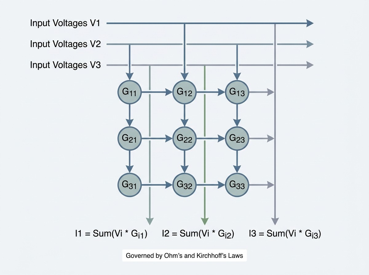
The conductanceof the memristive material at coordinate $(i, j)$ represents the synaptic weight. Vector-matrix multiplication (VMM) executes in a single $O(1)$ physical step via fundamental electronic circuit laws:
Ohm's Law: Applying an input voltage
across a memristor with conductance
generates a localized current:
Kirchhoff's Current Law: The individual currents along the common conductive column sum together automatically at the output node:
This physical calculation eliminates the need to fetch weight values into an ALU. However, practical memristor crossbars face engineering challenges:
Sneak-Path Currents: Unintended leakage currents bypass high-resistance junctions through adjacent low-resistance pathways, distorting current summation. Engineers mitigate this using One-Transistor-One-Resistor (1T1R) or selector-based crossbar topologies.
IR-Drop: Parasitic wire resistance along extended metal lines causes voltage drops, meaning downstream cells experience lower effective voltages than upstream cells.
Device Variability: Device-to-device (D2D) and cycle-to-cycle (C2C) variations in conductance, alongside stuck-at-fault (SAF) hardware defects, require noise-aware and fault-tolerant algorithmic training.
Training Spiking Neural Networks: Overcoming the Non-Differentiable Barrier
Spiking neural networks process spatio-temporal dynamics efficiently, but their non-linear threshold activation functions introduce mathematical challenges for gradient-based optimization.
The Heaviside Step Function and the Gradient Dilemma
Standard Artificial Neural Networks (ANNs) use smooth, continuous activation functions (such as GELU, SiLU, or Softmax) whose analytical derivatives are continuous and well-defined. In contrast, the spiking threshold is governed by the Heaviside step function, whose mathematical derivative is the Dirac delta function:
Under classical backpropagation, the gradient evaluates to zero almost everywhere across the network, causing gradient starvation. At the exact threshold boundary, the infinite gradient causes numerical explosion, preventing the convergence of gradient descent algorithms.
Direct Training via Surrogate Gradient Descent
To train SNNs end-to-end, researchers use Surrogate Gradients for Analog Neuromorphic Computing[4] within a Backpropagation Through Time (BPTT) framework. During the forward inference pass, the network retains its biological, non-linear step activation to maintain sparse binary spike dynamics. During the backward pass, the non-differentiable Dirac delta derivative is replaced with a smooth, continuous surrogate function:
Common surrogate formulations include:
Fast Sigmoid Derivative:
Arctangent Derivative:
By calculating continuous surrogate gradients through temporal states, frameworks such as snnTorch, SpikingJelly, and Norse integrate SNN graphs into modern automatic differentiation engines, making spiking models trainable via standard optimizers (such as AdamW).
# Conceptual PyTorch implementation of a Surrogate Gradient LIF Neuron
import torch
import torch.nn as nn

class SurrogateSpike(torch.autograd.Function):
    """
    Forward pass outputs a discrete binary step.
    Backward pass evaluates a continuous fast-sigmoid surrogate derivative.
    """
    @staticmethod
    def forward(ctx, membrane_potential, threshold=1.0, slope=10.0):
        ctx.save_for_backward(membrane_potential)
        ctx.threshold = threshold
        ctx.slope = slope
        return (membrane_potential >= threshold).float()

    @staticmethod
    def backward(ctx, grad_output):
        (membrane_potential,) = ctx.saved_tensors
        # Compute surrogate derivative: 1 / (1 + slope * |U - theta|)^2
        u_diff = torch.abs(membrane_potential - ctx.threshold)
        surrogate_grad = 1.0 / (1.0 + ctx.slope * u_diff) ** 2
        return grad_output * surrogate_grad, None, None

class LIFNeuronLayer(nn.Module):
    def __init__(self, decay_rate=0.85, threshold=1.0):
        super().__init__()
        self.decay_rate = decay_rate
        self.threshold = threshold
        self.spike_fn = SurrogateSpike.apply

    def forward(self, input_current, state=None):
        if state is None:
            state = torch.zeros_like(input_current)
        # Membrane dynamic: U[t] = decay * U[t-1] + I[t]
        updated_state = self.decay_rate * state + input_current
        spikes = self.spike_fn(updated_state, self.threshold)
        # Soft or hard reset: U[t] = U[t] * (1 - S[t])
        reset_state = updated_state * (1.0 - spikes)
        return spikes, reset_state
Model Conversion vs. Biologically Plausible Local Learning
Engineers deploy three primary paradigms for programming neuromorphic silicon:
ANN-to-SNN Conversion: A standard non-spiking neural network (such as a CNN with ReLU activations) is trained via conventional deep learning pipelines. The continuous ReLU activation magnitudes are mapped post-hoc to equivalent firing frequencies (rate coding) on spiking silicon. While this method requires no custom surrogate pipelines, it can introduce high temporal latency (often requiring 50 to 200 time steps per inference) and accuracy degradation during quantization.
Direct Supervised Spatio-Temporal Training: Directly training SNNs with surrogate gradients enables low latency (1 to 5 time steps per inference) and high task accuracy, though BPTT increases training-phase memory consumption.
On-Chip Synaptic Plasticity (STDP): Biologically plausible algorithms such as Spike-Timing-Dependent Plasticity adjust synaptic weights locally based on the microsecond correlation between presynaptic and postsynaptic spike timings:
Where. STDP enables local, unsupervised on-chip learning directly at the edge without calculating global loss gradients or storing deep computational backpropagation graphs.
Hardware Implementation Landscape: Digital vs. Analog Silicon
The neuromorphic hardware landscape spans fully digital, asynchronous implementations, analog physical emulators, and hybrid compute-in-memory ASICs.
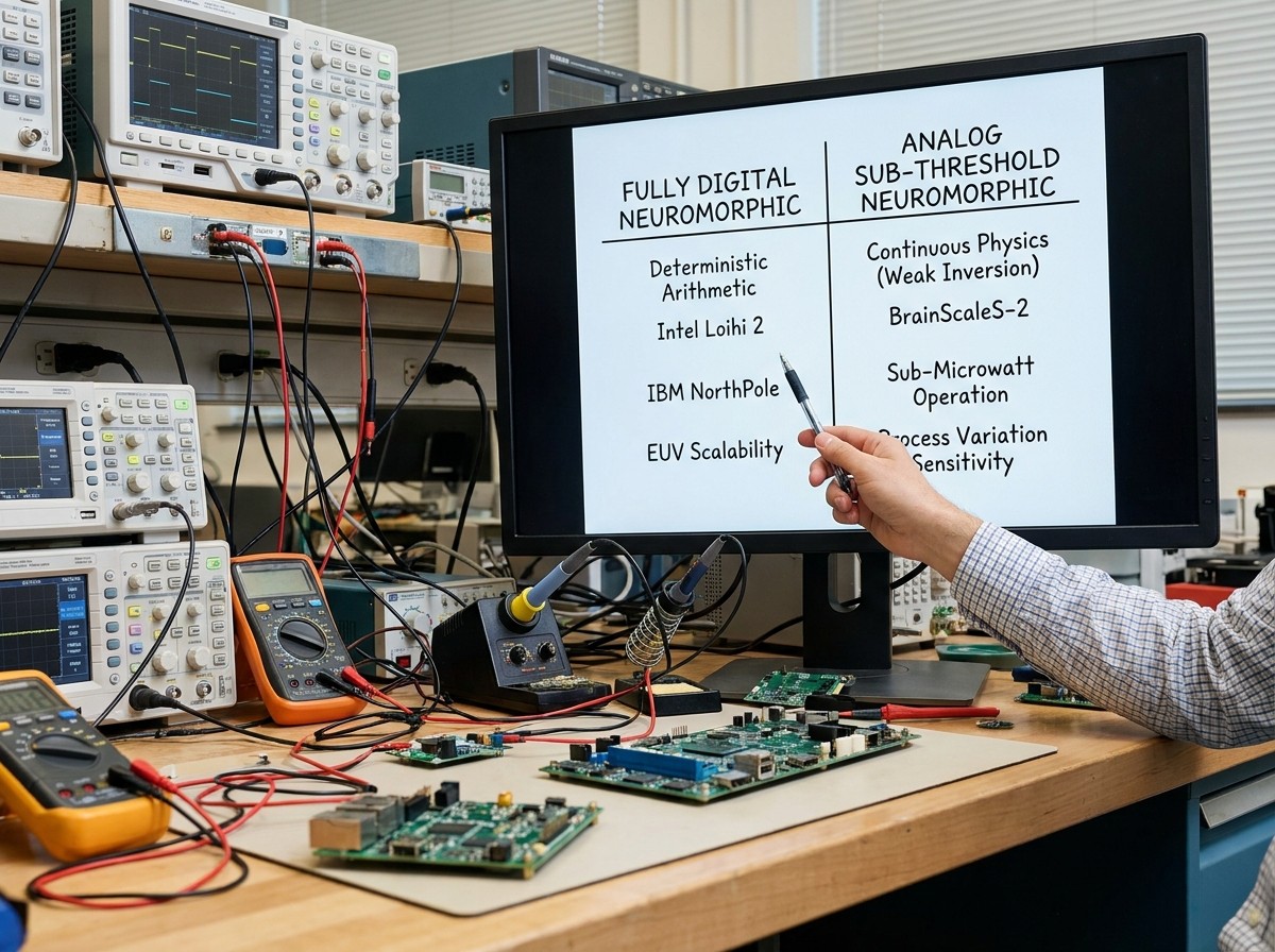
Digital Neuromorphic Processors
Digital neuromorphic silicon utilizes deterministic, clocked or unclocked logic gates to simulate differential membrane equations, ensuring reproducibility, noise tolerance, and compatibility with modern sub-7nm CMOS foundries.
Intel Loihi 2: Fabricated on the Intel 4 process (an EUV-based lithography node), the processor integrates 128 fully asynchronous neurocores and six embedded Lakemont microcontrollers within a 31 mm² die as detailed in Loihi: A Neuromorphic Manycore Processor with On-Chip Learning[1]. Containing 2.3 billion transistors, a single Loihi 2 chip supports up to 1.05 million programmable microcoded neuron models and up to 120 million individual synapses. The processor introduces an 8-bit graded spike architecture and operates within a sub-1 Watt power budget, yielding 30× to 100× higher energy efficiency on sparse sensory benchmarks compared to mobile GPUs.
IBM NorthPole: Demonstrating Neural inference at the frontier of energy, space, and time[2], IBM NorthPole is fabricated on a 12nm FinFET node with 22 billion transistors across an 800 mm² die, integrating 256 neural compute cores. It contains 224 MB of distributed on-chip SRAM (comprising a 192 MB core array and 32 MB frame buffer), achieving 13 TB/s of aggregate on-chip memory bandwidth. By eliminating reliance on off-chip DRAM during active inference, NorthPole achieves 25× higher energy efficiency (frames per Joule) and 22× lower latency on ResNet-50 computer vision benchmarks compared to equivalent 12nm baseline GPUs at w4a4 precision.
Analog and Mixed-Signal Neuromorphic Systems
Analog neuromorphic processors emulate biological ion channels by operating silicon transistors in the sub-threshold (weak inversion) physical domain. In this regime, the drain currentdepends exponentially on the gate-to-source voltage, mirroring the biophysics of biological cell membranes:
BrainScaleS-2: Developed at Heidelberg University, this mixed-signal platform uses analog circuits to solve continuous-time differential equations at physical speeds
faster than biological real time. It supports up to 512 analog neuron circuits and 130,000 synapses per chip, delivering sub-microwatt energy scaling for high-speed physical simulation.
Engineering Trade-offs: Analog neuromorphic silicon achieves lower energy consumption than digital equivalents for continuous dynamical systems. However, it remains susceptible to thermal drift, transistor mismatch, process-voltage-temperature (PVT) variations, and low signal-to-noise ratios (SNR), complicating deterministic debugging and post-fabrication software compilation.
Comparative Hardware Evaluation Matrix
| Processor Platform | Silicon Node | Architecture Class | Neuron / Synapse Capacity | Compute Mechanism | Target Workloads & Primary Optimization |
|---|---|---|---|---|---|
| Intel Loihi 2 | Intel 4 (EUV) | Fully Digital Asynchronous | Up to 1.05M Neurons / 120M Synapses | Event-driven microcoded neurocores | Dynamic sensor fusion, sparse robotics, adaptive edge learning |
| IBM NorthPole | 12nm FinFET | Digital Compute-in-Memory | 256 Cores / 224MB On-Chip SRAM | Distributed SRAM-ALU vector fabric | Low-latency computer vision (ResNet, YOLO), edge video streams |
| SpiNNaker-2 | 22nm FD-SOI | Manycore Hybrid Digital | 152 ARM Cortex-M4F cores per chip | Software-programmable SNN/ANN simulation | Large-scale brain simulation, computational neuroscience |
| BrainScaleS-2 | 65nm CMOS | Analog Sub-threshold | 512 Analog Neurons / 130k Synapses | Physical continuous-time analog emulation | High-speed bio-signal emulation, ultra-low power physics |
| BrainChip Akida AKD1500 | 28nm / 16nm | Digital Event-Domain NPU | Multi-node neural fabric | Event-driven integer/spike processing | Ultra-low power edge IoT, audio classification, vibration sensing |
Real-World Applications: Where Neuromorphic Silicon Outperforms GPUs
Neuromorphic silicon provides structural advantages in applications where physical data arrives continuously, asynchronously, and sparsely from the operational environment.
What is Neuromorphic Chip and How it Works? | L-10 | Semiconductor Chips
Event-Based Vision and Dynamic Vision Sensors (DVS)
Standard video cameras capture visual information at fixed frame rates (e.g., 30 to 120 Hz), repeatedly transmitting static background pixels and saturating bus channels with redundant data as highlighted in a comprehensive Review of spike-based neuromorphic computing for brain-inspired vision: biology, algorithms, and hardware[7]. Dynamic Vision Sensors (such as the Sony-Prophesee IMX636) operate with autonomous, decoupled pixels that emit an asynchronous event tupleonly when the local change in logarithmic illumination exceeds an adjustable threshold:
Comparing frame cameras with event sensors highlights dramatic operational contrasts:
Frame Cameras (30–120 Hz): Transmit continuous 2-megapixel grids with over 90% redundant static background, suffer from motion blur during rapid maneuvers, and provide dynamic range limited to ~60 dB.
Event-Based Cameras: Stream sparse microsecond tuples with temporal resolution below 15 µs, achieve ultra-wide dynamic range above 120 dB, and consume only 10 mW to 32 mW of active sensor power.
Because neuromorphic chips ingest AER event packets directly, the pairing of event cameras with neuromorphic processors eliminates frame-buffering latency. Research across edge robotics demonstrates optical flow estimation and monocular depth prediction with sub-millisecond latencies (<0.5 ms) while operating within milliwatt power budgets.
High-Speed Closed-Loop Autonomous Robotics and Drones
Traditional robotic architectures introduce closed-loop latency (typically 20 to 100 ms) through sequential frame grabbing, tensor formatting, GPU batch inference, and proportional-integral-derivative (PID) motor translation. Under high angular velocities, this latency creates instability in agile platforms.
Neuromorphic processors execute real-time state estimation and reflex loops within sub-millisecond windows. In visual stress evaluations, autonomous robotic arms and multi-rotor drones use neuromorphic vision pipelines to execute precise maneuvers—such as landing on moving targets or avoiding obstacles in GPS-denied environments—while drawing less than 2 Watts of compute power.
Continuous Biomedical Signal Monitoring and Spaceborne Edge Computing
Implantable and Wearable Medical Devices: High-density electromyography (EMG) and electroencephalography (EEG) monitoring require continuous multi-channel inference. Standard GPUs exceed safe thermal dissipation thresholds for implantable biosensors. Neuromorphic microcontrollers execute real-time seizure detection and prosthetic motor decoding on microwatt-scale power budgets, preventing tissue heating.
Aerospace and Spaceborne Autonomy: CubeSats and interplanetary probes operate under severe Size, Weight, and Power (SWaP) constraints and high ionizing radiation fields. Through the 3D Integrated Memristor Chip for Neuromorphic Processing[6] initiative, NASA evaluates 3D integrated memristor crossbars and neuromorphic ASICs for low-power edge autonomy, enabling real-time anomaly detection without relying on ground-station telemetry links.
What Developers and Researchers Report on Community Forums
Engineering discussions across developer forums and open-source repositories highlight several practical realities when transitioning from deep learning frameworks to spiking hardware:
The ANN-to-SNN Accuracy Drop: Practitioners consistently report that converting dense convolutional networks to spiking formats via rate coding often leads to a 2% to 7% reduction in classification accuracy unless the model is retrained with quantization-aware surrogate gradient loops.
Temporal Sizing Complexities: In libraries like
snnTorchandSpikingJelly, debugging the trade-off between time-step depth () and task latency requires empirical tuning. Setting
too low degrades predictive capacity, while setting
too high increases training time and memory overhead during BPTT.
Lack of Universal Hardware Compilers: Developers emphasize that transferring models trained in PyTorch to physical targets (such as Loihi 2 via Intel Lava or Akida via MetaTF) requires hardware-specific graph transformations, illustrating the need for unified compilation standards.
The Architectural Reality: Why Neuromorphic Silicon Has Not Replaced GPUs
Despite their energy efficiency advantages in streaming applications, neuromorphic chips have not displaced GPUs in mainstream datacenter deep learning and Large Language Models (LLMs) due to architectural, mathematical, and algorithmic differences.
The Transformer Matrix Multiplication Mismatch
Autoregressive Large Language Models (such as GPT-4, Llama 3, or Claude) rely fundamentally on the dense Scaled Dot-Product Attention mechanism:
This formulation presents several structural challenges for neuromorphic architectures:
Dense Vector Interdependencies: Every token in a sequence must calculate mathematical dot products against every other token, generating dense, fully connected tensor graphs rather than sparse, localized spatio-temporal spike trains.
Precision and Dynamic Range: Generative language models require high numerical precision (FP16, BF16, or quantized INT8/FP4 formats) to prevent degradation in language modeling perplexity. Spiking architectures represent high-precision values by accumulating pulses over extended time horizons (
), which increases operational latency and counteracts their energy advantages.
Hardware Utilization at Batch: Datacenter GPUs achieve near-complete silicon utilization when processing large batch sizes (
), maximizing floating-point operations per second per dollar. Neuromorphic architectures are optimized for batch size
streaming data, losing their relative throughput advantage in high-throughput offline batch training.
The Software Toolchain and Compilation Chasm
NVIDIA’s software ecosystem (comprising CUDA, cuDNN, TensorRT, and Triton) represents over fifteen years of specialized compiler optimization, kernel engineering, and framework integration. In contrast, the neuromorphic ecosystem has historically faced fragmentation across proprietary, hardware-specific SDKs.
To address this challenge, the neuromorphic community is developing standardized frameworks:
Neuromorphic Intermediate Representation (NIR): A standardized, open computational graph format that enables models defined in
snnTorchorSpikingJellyto compile down to hardware platforms without requiring ground-up rewrites.The NeuroBench Framework: Established by an international consortium to advance standard evaluation via NeuroBench: Advancing Neuromorphic Computing through Collaborative, Fair and Representative Benchmarking[5], this initiative provides multi-track criteria across algorithmic sparsity, synaptic operations per inference, and hardware energy-delay products (EDP).
Hybrid Computing Architectures
The computing landscape is moving toward heterogeneous integration rather than single-architecture dominance. In these systems:
Host GPUs and Cloud Accelerators perform high-throughput, dense datacenter training, complex multi-modal reasoning, and batch Transformer calculations.
Neuromorphic Coprocessors operate at the physical edge, ingesting high-frequency sensory data, running always-on monitoring routines, and executing sub-millisecond reflex loops under strict sub-Watt thermal limits.
Developer Decision Framework and Architectural Selection
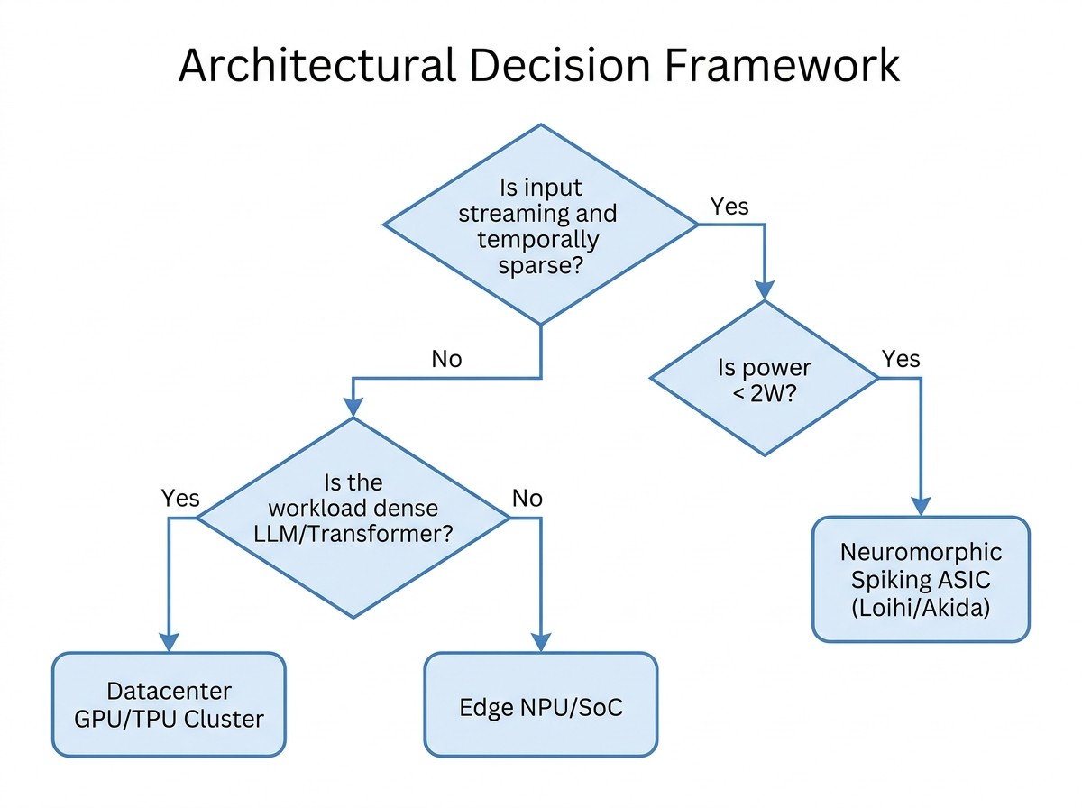
Choosing between conventional synchronous accelerators, compute-in-memory ASICs, and neuromorphic processors depends on input temporal sparsity, latency budgets, and deployment power constraints.
Architectural Trade-off Checklist
Select Neuromorphic Spiking Silicon (e.g., Intel Loihi 2, BrainChip Akida) if:
The sensor pipeline uses event-driven hardware (such as Dynamic Vision Sensors or continuous bio-signal arrays).
The application requires sub-5 millisecond response latency at batch size
.
Total compute power is restricted to milliwatt or single-digit Watt envelopes.
The system processes sparse temporal data streams where information arrives intermittently.
Select Digital Compute-in-Memory ASICs (e.g., IBM NorthPole) if:
The workload consists of standard non-spiking computer vision networks (ResNet, YOLO).
The priority is eliminating off-chip DRAM latency without redesigning models into spiking formats.
The model weights fit within available on-chip SRAM capacity (typically
).
Select Synchronous GPUs / TPUs if:
The workload involves autoregressive language modeling, dense attention mechanisms, or large foundational transformers.
The primary task is high-throughput offline batch training over large datasets.
Development requires direct integration with mature CUDA libraries, distributed scaling, and standard automatic differentiation workflows.
Synthesis and Getting Started
Neuromorphic computing provides a physically distinct alternative to the von Neumann architecture, solving the memory wall through co-located synaptic memory and event-driven computation. While unsuited to replace GPUs for dense transformer matrix processing, it offers significant latency and energy advantages for real-time, streaming edge intelligence.
Developer Next Steps and Tooling
To begin developing with spiking architectures and neuromorphic algorithms:
Model Prototyping in PyTorch:
Explore
snnTorchfor tutorial workflows covering surrogate gradient descent and LIF neuron implementations.Use
SpikingJellyfor high-performance CUDA-accelerated deep spiking network training.Hardware-Agnostic Compilation:
Review the
Neuromorphic Intermediate Representation (NIR)specifications to understand graph conversion across hardware targets.Explore Intel’s open-source
Lava Software Frameworkfor building asynchronous event-driven applications.Standardized Benchmarking:
Review the algorithmic and hardware evaluation suites maintained by the
NeuroBenchconsortium to benchmark model sparsity, compute energy, and execution latency.
Technical FAQ
How does a Spiking Neural Network encode continuous real-world sensor data into discrete spikes?
SNNs encode continuous data through three primary methods:
Rate Coding: Maps analog continuous values to proportional spike frequencies over a fixed time window. While robust against single-spike noise, it requires longer accumulation times and higher overall switching energy.
Temporal / Time-to-First-Spike Coding: Encodes signal intensity in the precise timing of a single spike relative to a reference signal (where higher amplitudes spike earlier), achieving higher information density per event.
Direct Graded Spikes: Used in architectures like Intel Loihi 2, graded spiking allows events to carry multi-bit integer or floating-point payloads $(x, y, t, p)$, encoding continuous values directly without multi-timestep latency penalties.
Can neuromorphic chips execute standard convolutional or transformer architectures?
Standard convolutional networks can run on neuromorphic silicon via ANN-to-SNN conversion or direct surrogate gradient training with 1D/2D spiking convolutional layers. Non-spiking digital compute-in-memory architectures (such as IBM NorthPole) execute standard INT8/INT4 convolutional models natively without converting activations to spikes. However, dense multi-head self-attention mechanisms in transformers map inefficiently to event-based architectures due to their all-to-all connectivity and high dynamic range requirements.
What is the primary difference between digital and analog neuromorphic hardware?
Digital neuromorphic systems (such as Intel Loihi 2) use deterministic arithmetic logic gates to simulate differential membrane potential equations, providing high noise immunity, reproducibility, and scalability across standard CMOS nodes. Analog neuromorphic systems (such as BrainScaleS-2) use the sub-threshold physics of transistors to continuously emulate physical cell membrane dynamics, offering extreme low-power performance while remaining susceptible to thermal noise, fabrication mismatch, and device variability.
How do memristive crossbar arrays eliminate the von Neumann bottleneck?
Memristive crossbars eliminate data shuttling by performing analog vector-matrix multiplication directly inside non-volatile memory junctions. Input activations applied as voltages along crossbar rows interact with the conductance of the memristive material via Ohm’s Law (), and the resulting currents aggregate along columns via Kirchhoff’s Current Law () in a single physical time step.
Why does surrogate gradient descent make SNNs practical for machine learning workflows?
The biological spike threshold function is non-differentiable because its mathematical derivative is zero everywhere except at the exact threshold, where it goes to infinity. Surrogate gradient descent retains the discrete step function during forward inference, but replaces the non-differentiable derivative with a smooth, continuous mathematical approximation during the backward pass. This allows modern autograd engines (like PyTorch) to optimize spatio-temporal spiking networks via standard gradient descent and AdamW optimizers.
References
Loihi: A Neuromorphic Manycore Processor with On-Chip Learning — IEEE Micro / Intel Labs
Neural inference at the frontier of energy, space, and time — Science / IBM Research
Spiking Neural Networks Hardware Implementations and Challenges: A Survey — ACM Journal on Emerging Technologies in Computing Systems
Surrogate Gradients for Analog Neuromorphic Computing — Proceedings of the National Academy of Sciences (PNAS)
NeuroBench: Advancing Neuromorphic Computing through Collaborative, Fair and Representative Benchmarking — National Institute of Standards and Technology (NIST)
3D Integrated Memristor Chip for Neuromorphic Processing — National Aeronautics and Space Administration (NASA)
Review of spike-based neuromorphic computing for brain-inspired vision: biology, algorithms, and hardware — SPIE Digital Library
Memristor Crossbar Array with Enhanced Device Yield for In-Memory Vector-Matrix Multiplication — ACS Applied Electronic Materials / American Chemical Society
 UTMEL
UTMEL
We are the professional distributor of electronic components, providing a large variety of products to save you a lot of time, effort, and cost with our efficient self-customized service. careful order preparation fast delivery service
 Improving the Energy Conversion Efficiency of Triboelectric NanogeneratorsSaumitra Jagdale19 November 20243312
There is a huge growth in demand for self-sustaining electronic devices, as the traditional power-generating devices fail in remote and harsh environments due to the periodic requirement of battery changes. Also, these devices are frequency specific; some work only in high frequency and some in low frequency. Triboelectric nanogenerators (TENGs) provide a promising solution by efficiently converting mechanical energy into electricity as they are versatile, compact, and cheap, making them a popular choice.
Read More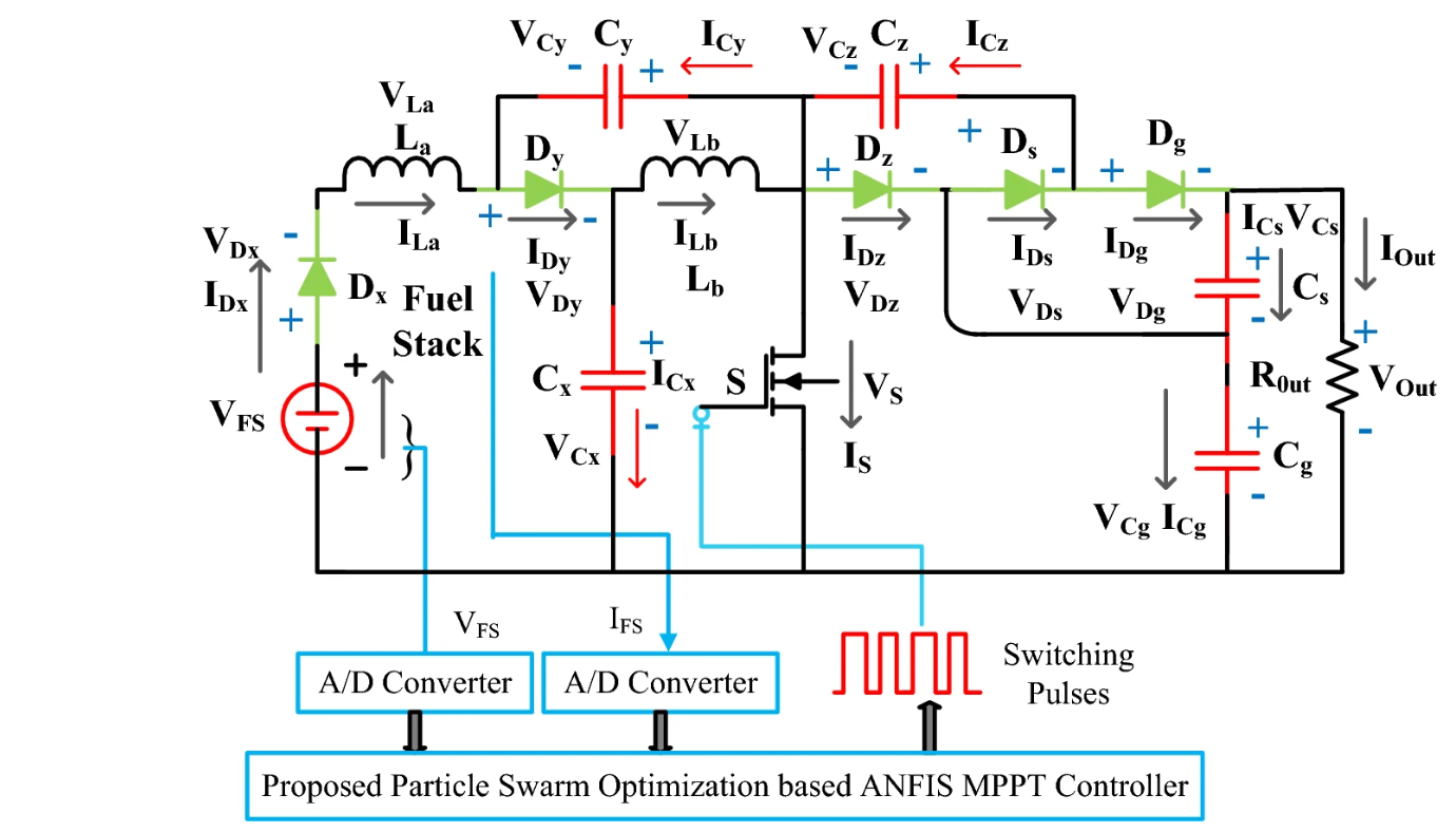 Methodologies for Increasing Efficiency of Fuel Stack Technology for Energy GenerationSaumitra Jagdale19 November 20243155
Presently, power companies are moving towards renewable energy systems. Conventional energy sources are more expensive because they require a vast network to be maintained and huge human resources. Also, they harm the environment by releasing several harmful gases. As the industry’s focus shifts toward renewable energy sources, energy systems powered by Proton Exchange Membrane Fuel Stacks (PEMFS) are gaining traction.
Read More VSC Light Meaning, Causes, and Step-by-Step DiagnosticsUTMEL19 May 20264304
A VSC (Vehicle Stability Control) light indicates the system is disabled, often as a fail-safe triggered by unrelated engine faults like a loose gas cap. While the stability system prevents lateral skidding, it shuts down when sensor data is unreliable. Proper diagnosis requires an ABS-capable OBD2 scanner. Resolving the root engine code, checking wheel speed sensors, or performing a zero-point calibration usually restores system function.
Read More What JEDEC JEP203 and JEP204 Actually Change for SiC Qualification Engineers and Component BuyersUTMEL29 July 2026573
Summary: When JEDEC published JEP203 and JEP204 on June 3, 2026[1], most coverage treated them as an announcement. They are better understood as the first shared language the silicon carbide industry has had for two problems that have quietly consumed engineering hours since the first commercial SiC MOSFETs shipped: short-circuit evaluation that produces numbers you can compare across suppliers, and a consolidated reference of stress procedures so qualification engineers stop reinventing test plans from scratch. This article explains what changes on Monday morning and what to ask suppliers for now.
Read More 2nm vs 3nm Chips: What the Latest Process Nodes Mean for PerformanceUTMEL19 August 20262092
The shift from 3nm to 2nm process nodes marks a fundamental change in transistor architecture, moving from FinFET to Gate-All-Around (GAA) nanosheets. This transition delivers meaningful improvements in performance, power, and density, but also introduces new challenges like SRAM scaling limits, thermal density, and backside power delivery. The article compares TSMC, Samsung, and Intel approaches, offering a practical decision framework for engineering teams.
Read More
Subscribe to Utmel !
![47-20029]() 47-20029
47-20029Amphenol RF
![1212086]() 1212086
1212086Phoenix Contact
![0638853300]() 0638853300
0638853300Molex
![2002180200]() 2002180200
2002180200Molex
![121586-5229]() 121586-5229
121586-5229ITT Cannon, LLC
![CD-800-13]() CD-800-13
CD-800-13Panduit Corp
![AA-400-200-CE-SUPRHTR]() AA-400-200-CE-SUPRHTR
AA-400-200-CE-SUPRHTRTE Connectivity Aerospace, Defense and Marine
![1212321]() 1212321
1212321Phoenix Contact
![2150289-1]() 2150289-1
2150289-1TE Application Tooling
![1204038]() 1204038
1204038Phoenix Contact


