MOSFET vs. IGBT: Characteristics, Structure and Market Analysis

MOSFET BJT or IGBT - Brief comparison Basic components
Catalog |
Ⅰ What is a MOSFET?
Field-Effect Transistors (FETs) are primarily categorized into two main types: JFET (Junction Field-Effect Transistor) and MOSFET.
MOSFET stands for Metal-Oxide-Semiconductor Field-Effect Transistor. It is also referred to as an Insulated-Gate Field-Effect Transistor (IGFET) because the gate terminal is electrically isolated from the channel by a thin insulating oxide layer.
MOSFETs are generally classified into four distinct categories based on their operation mode and channel type:
① N-channel Depletion Mode;
② N-channel Enhancement Mode (most common in power electronics);
③ P-channel Depletion Mode;
④ P-channel Enhancement Mode.

MOSFET types and circuit symbols
Most power MOSFETs contain an intrinsic body diode (also known as a parasitic diode) connected between the drain and source.
The primary role of this parasitic diode is protection and freewheeling. In inductive load applications (like motor drives), it provides a path for back-EMF current when the transistor switches off, preventing high voltage spikes from exceeding the breakdown voltage (VDSS) and burning out the MOSFET.
Key characteristics of MOSFETs include extremely high input impedance, fast switching speeds, and good thermal stability. They are voltage-controlled devices, widely used as electronic switches in high-frequency power supplies and amplifiers.
Ⅱ What is an IGBT?
IGBT (Insulated Gate Bipolar Transistor) is a composite semiconductor device that combines the best attributes of a BJT (Bipolar Junction Transistor) and a MOSFET.
As a robust power semiconductor, the IGBT features the high input impedance of a MOSFET (easy to drive) and the low conduction loss of a BJT (high current capability). This makes it ideal for high-voltage, high-current applications.

IGBT and circuit symbol
Circuit symbols for IGBTs can vary, often borrowing elements from both triodes and MOSFETs. In schematics, the specific model number is usually the best indicator of whether a device is an IGBT or a MOSFET.
Crucially, standard IGBTs do not inherently have a body diode like MOSFETs. However, many modern IGBTs are packaged with an anti-parallel diode (Freewheeling Diode or FWD) to protect the device from reverse currents. Always verify the datasheet to confirm if an internal diode is present.

Integrated Freewheeling Diode (FWD)
You can check for this diode using a multimeter. If the resistance between the Collector (C) and Emitter (E) is infinite in both directions, no diode is present. If it conducts in one direction, the package includes an FWD.
IGBTs are the dominant choice for AC motor drives, traction inverters (trains/EVs), switching power supplies, and induction heating where voltage exceeds 600V.
Ⅲ Structural of MOSFET and IGBT
The internal physical structure of MOSFETs and IGBTs is similar, but with a critical difference in the substrate layers.

Internal structure of MOSFET and IGBT
The IGBT adds a P+ injection layer to the drain side of the standard MOSFET structure. This additional layer injects holes into the drift region, significantly reducing on-state resistance (conductivity modulation).
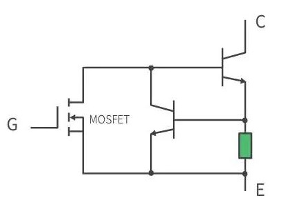
The ideal equivalent circuit (below) visualizes the IGBT as a MOSFET driving a transistor (BJT). This allows the IGBT to handle high voltages with very low saturation voltage (VCE(sat)), overcoming the high RDS(on) issue typical of high-voltage MOSFETs.

IGBT ideal equivalent circuit
However, this structure introduces a "current tail" during turn-off, making IGBTs slower than MOSFETs. The charge storage effect in the BJT section necessitates a longer dead time in switching circuits, limiting the maximum switching frequency.
Ⅳ MOSFETs or IGBTs: Which one should we use?
Selecting between a MOSFET and an IGBT depends on system voltage, current requirements, and switching frequency. In 2025, engineers must also consider Silicon Carbide (SiC) and Gallium Nitride (GaN) devices, which are challenging traditional silicon roles.

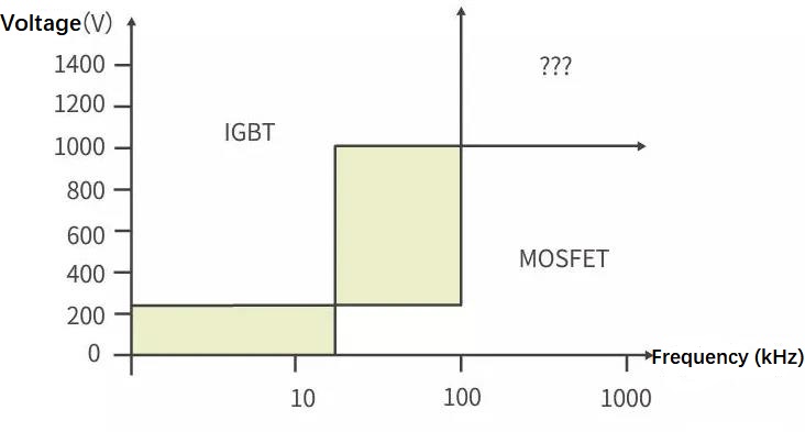
MOSFET and IGBT application characteristics
The chart below illustrates the traditional operating boundaries. The shaded area represents overlap where either device could work, though efficiency will vary.

Common Application Areas for MOSFETs and IGBTs
Summary of Selection Criteria:
MOSFETs (Silicon): Best for low voltage (<250V) and high frequency (>100kHz). They are ideal for battery protection, low-power SMPS, and consumer electronics.
IGBTs: Best for high voltage (>600V to 6.5kV) and high current at lower frequencies (<20kHz). They dominate in electric vehicle (EV) traction inverters, industrial motor drives, and renewable energy grid ties.
Emerging Tech (SiC & GaN): In 2025, SiC MOSFETs are increasingly replacing IGBTs in 800V EV architectures due to superior efficiency. GaN is taking over the consumer adapter market (e.g., fast chargers) due to its high density.
If your application requires switching speeds in the MHz range, MOSFETs (or GaN) are the only viable option. For heavy-duty industrial switching where robustness and cost per watt are paramount, the IGBT remains the king.
Ⅴ Identification of MOSFET and IGBT
Because MOSFETs and IGBTs often share identical packages (like TO-247 or TO-220), they look nearly identical. Manufacturers sometimes use obscure markings, or the markings may be erased in proprietary circuits. Here is how to distinguish them using a multimeter.
Note: The pin mapping is usually Gate (1), Drain/Collector (2), Source/Emitter (3).
Static Measurement (Resistance Mode)
First, short-circuit all pins to discharge any static or gate capacitance.
1. Check for Body Diode: Measure resistance between pin 2 and pin 3.
MOSFET: You will detect a diode drop (finite resistance) in one direction (Source to Drain) due to the intrinsic body diode.
IGBT: If it is a non-FWD IGBT, resistance will be infinite in both directions. If it is an IGBT with a co-packaged diode, it will behave like the MOSFET.
2. Check Gate Isolation: Measure resistance between Gate (1) and other pins. Both devices should show infinite resistance. If you read a low value, the device is damaged (oxide breakdown).
Dynamic Measurement (Trigger Test)
Use the multimeter's diode mode or a small voltage source to charge the Gate.
Touch the positive probe to the Gate and negative to the Source/Emitter to charge the gate capacitance.
Quickly move probes to measure the Drain-Source (or Collector-Emitter) path.
MOSFET: The RDS(on) is extremely low (near zero ohms).
IGBT: You will measure a voltage drop (VCE(sat)) typically around 0.3V to 0.7V in this test mode, but not a pure "zero ohm" short like a MOSFET, due to the PN junction characteristics.
This dynamic difference—resistive vs. junction drop—is the most reliable way to differentiate them without seeing the part number.
Ⅵ MOSFET and IGBT Market Analysis (2025 Update)
Power semiconductors remain the backbone of modern energy conversion, critical for electric vehicles (EVs), renewable energy systems, and AI data centers.
The market is broadly divided into Power Discretes and Power Integrated Circuits (Power ICs). As of 2024, the global power semiconductor market was valued at approximately $50 billion and is projected to exceed $70 billion by 2032.
Market Drivers: Automotive and Green Energy
The demand landscape has shifted dramatically. While industrial control remains a massive sector (approx. 34%), the automotive sector is the fastest-growing driver due to vehicle electrification.
According to recent 2025 market reports:
The combined market for IGBTs and Super Junction MOSFETs was valued at roughly $16.3 billion in 2024.
Market growth is expected to continue at a CAGR of over 8-12% through 2030.
MOSFETs continue to dominate low-voltage applications. They are essential in automotive auxiliary systems, consumer electronics, and increasingly in AI server power supplies (DC-DC conversion).
IGBTs maintain a stronghold in high-power applications. Despite the rise of SiC, IGBTs remain the cost-effective standard for wind turbines, solar inverters, and mass-market EV inverters.

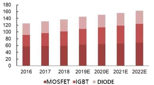
*Note: Historical trajectory shown.Current 2025 values have surpassed these early estimates.*
The Electric Vehicle Revolution
The transition from Internal Combustion Engines (ICE) to Electric Vehicles (EVs) has multiplied the value of semiconductors per vehicle.
In a traditional fuel car, power semiconductors account for only about 20% of the semiconductor content. However, in a Battery Electric Vehicle (BEV), this figure skyrockets.
By 2025, the power semiconductor content in a standard BEV is estimated to be $450 to $500 per vehicle—roughly 5 to 6 times that of a traditional car. The total semiconductor value in premium EVs now frequently exceeds $1,000.
The Rise of SiC: A major trend in 2025 is the adoption of Silicon Carbide (SiC) MOSFETs in 800V EV architectures. While more expensive than IGBTs, SiC allows for faster charging and longer range, justifying the cost for premium manufacturers.
In summary, while silicon MOSFETs and IGBTs remain the workhorses of the industry, the market is evolving toward higher efficiency solutions like SiC and GaN to meet global net-zero energy goals.
1.Which is better MOSFET or IGBT?
When compared to the IGBT, a power MOSFET has the advantages of higher commutation speed and greater efficiency during operation at low voltages. What's more, it can sustain a high blocking voltage and maintain a high current. This is because most power MOSFETs structures are vertical (not planar).
2.Can MOSFET replace IGBT?
Due to the higher usable current density of IGBTs, it can usually handle two to three times more current than a typical MOSFET it replaces. This means that a single IGBT device can replace multiple MOSFETs in parallel operation or any of the super-large single power MOSFETs that are available today.
 MOSFET vs. IGBT: Characteristics, Structure and Market AnalysisUTMEL25 December 202521282
With the rise of new energy in recent years, the market demand for MOSFETs and IGBTs is increasing steeply. Generally used as switching devices, they are widely used in electronic circuits. MOSFETs and IGBTs are relatively similar in appearance and characteristics parameters. So what is the difference between MOSFETs and IGBTs?
Read More Introduction to FinFETUTMEL18 March 202128975
The full name of FinFET is Fin Field-Effect Transistor. It is a new complementary metal oxide semiconductor transistor. The FinFET name is based on the similarity between the shape of the transistor and the fin.
Read More What is a MOSFET?UTMEL16 April 20216872
MOSFET, short for Metal-Oxide-Semiconductor Field-Effect Transistor, is a field-effect transistor that can be widely used in analog circuits and digital circuits. MOSFETs can be divided into N-channel type with the majority of electrons and P-channel type with the majority of holes according to their "channel" polarity. They are usually called NMOSFET and PMOSFET.
Read More NPN Transistors and PNP TransistorsUTMEL29 October 20209106
NPN and PNP are two types of transistors. Transistors are semiconductor devices made of doped p-type and n-type junctions. This article mainly introduces the differences between this two kinds of transistors, the methods of distinguishing them, and the application of them.
Read More An Overview of Bipolar TransistorsUTMEL27 August 20208300
Bipolar Transistor, full name bipolar junction transistor(BJT), is an electronic device with three terminals, made of three parts of semiconductors with different levels of doping. The charge flow in the transistor is mainly due to the diffusion and drift movement of carriers at the PN junction.
Read More
Subscribe to Utmel !
![H200X064H1T-2-B]() H200X064H1T-2-B
H200X064H1T-2-BPanduit Corp
![GRM31BR73A102KW01L]() GRM31BR73A102KW01L
GRM31BR73A102KW01LMurata Electronics
![LQG15HH27NH02D]() LQG15HH27NH02D
LQG15HH27NH02DMurata Electronics
![SLB-25MG3F]() SLB-25MG3F
SLB-25MG3FROHM Semiconductor
![PEC11R-4220F-S0024]() PEC11R-4220F-S0024
PEC11R-4220F-S0024Bourns Inc.
![BLM03AX121SZ1D]() BLM03AX121SZ1D
BLM03AX121SZ1DMurata Electronics
![101020057]() 101020057
101020057Seeed Technology Co., Ltd
![ST2-DC24V-F]() ST2-DC24V-F
ST2-DC24V-FPanasonic Electric Works
![SR732ATTD6R80F]() SR732ATTD6R80F
SR732ATTD6R80FKOA Speer Electronics, Inc.
![EMK107BJ225KA-T]() EMK107BJ225KA-T
EMK107BJ225KA-TTaiyo Yuden


 Product
 Brand
Brand Articles
 Tools
Tools


