

 Product
 Brand
Brand Articles
 Tools
Tools
What Is a MOSFET? Working Principle, Types, and Selection Guide
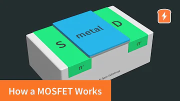
How a MOSFET Works - with animation! | Intermediate Electronics
A MOSFET is one of the most common building blocks in modern electronics, sitting inside everything from a phone charger to a motor drive. The name stands for metal-oxide-semiconductor field-effect transistor, and the long name actually describes how the device is built and how it behaves: a voltage applied to an insulated gate sets up an electric field that controls how easily current flows through a channel. That single idea, voltage in, current control out, is what makes the part so useful as both a switch and an amplifier.
How a MOSFET Works
A MOSFET has three working terminals: the gate, the drain, and the source. The gate sits over the semiconductor body but is separated from it by a very thin insulating oxide layer. Because of that insulation, the gate does not draw a steady current the way a control input might in other devices; instead it behaves like one plate of a small capacitor. When you raise the gate voltage relative to the source, the resulting electric field reaches through the oxide and rearranges charge in the semiconductor underneath.
Below a certain gate-to-source voltage, called the threshold, the device stays effectively off and only a tiny leakage flows. Once the gate voltage passes the threshold, the field pulls enough charge carriers toward the surface to form a conductive channel between drain and source. The further the gate voltage rises past the threshold, the more strongly the channel conducts. This is why a MOSFET is described as voltage-controlled: the gate-source voltage, not a gate current, decides whether and how hard the channel turns on.
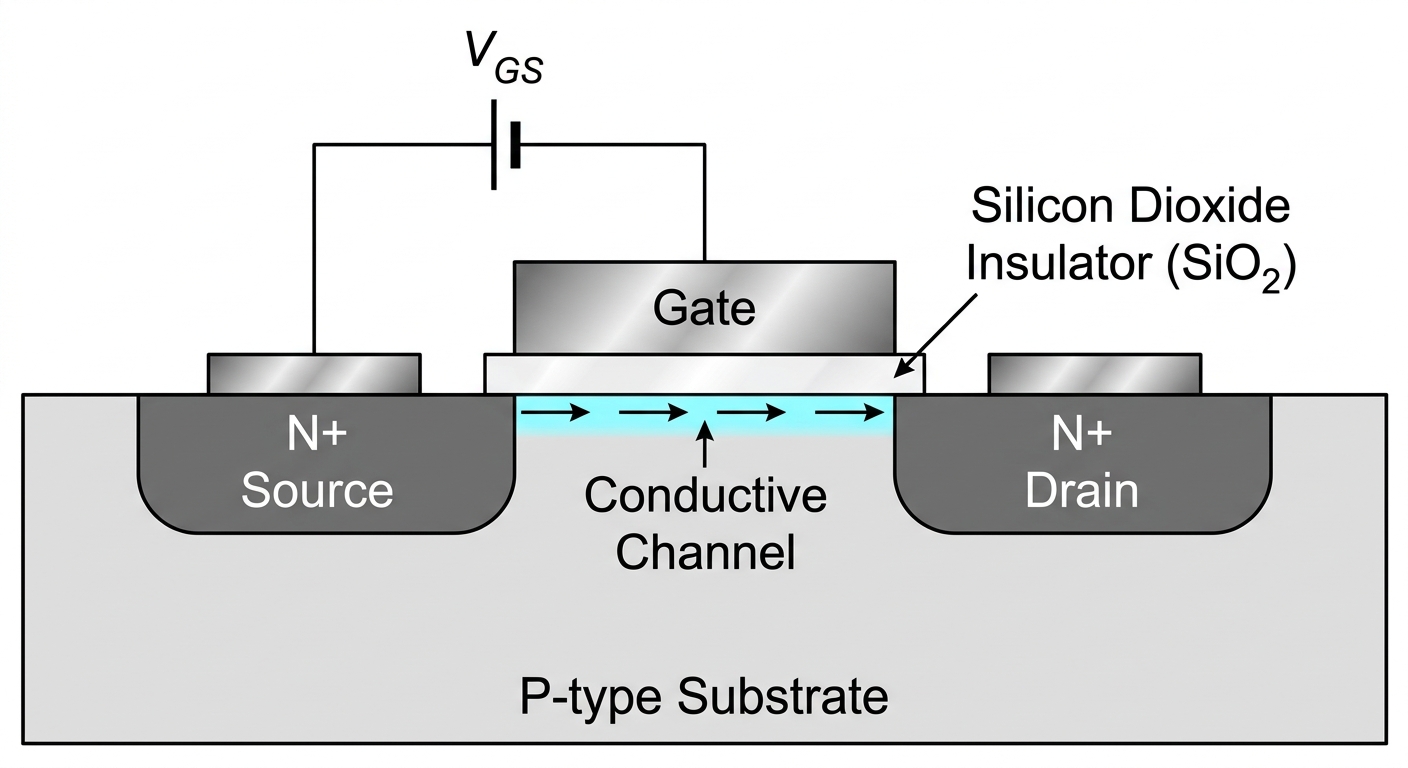
Figure 1: Internal cross-section of an N-channel enhancement-mode MOSFET. Applying a positive gate voltage creates an electric field that forms a conductive electron channel between the source and drain.
The thin gate oxide is the reason the input impedance is so high, and it is also the part's most delicate feature. The same insulation that lets the gate steer the channel with almost no steady current is easily damaged if the gate voltage is pushed too far, a theme that returns in the failure section below.
MOSFET vs a Regular Bipolar Transistor
A bipolar junction transistor (BJT) and a MOSFET can both act as switches or amplifiers, but they are controlled in fundamentally different ways. A BJT is current-controlled: you push a base current into it, and that current commands a larger collector current. A MOSFET is voltage-controlled: you set a gate voltage, and the field it creates governs the channel. The practical consequences of that difference shape which device an engineer reaches for.
| Aspect | MOSFET | Bipolar transistor (BJT) |
|---|---|---|
| Control quantity | Gate-to-source voltage | Base current |
| Input behaviour | High input impedance, capacitive gate | Lower input impedance, draws base current |
| Steady-state drive effort | Very small once charged | Continuous base current while on |
| Conduction character | Resistive channel when on | Roughly fixed voltage drop across the junction |
| Typical strengths | Fast switching, simple voltage drive | Linear behaviour, low offset at low currents |
Because the gate is insulated, holding a MOSFET on costs almost no steady drive power once the gate capacitance is charged. A BJT, by contrast, needs ongoing base current to stay on. That distinction is a large part of why MOSFETs dominate switching power circuits, while bipolar devices still earn their place in certain analog and small-signal roles.
The Four Types of MOSFET
MOSFETs are sorted along two independent axes, and combining them gives the four standard types. The first axis is channel polarity, N-channel or P-channel, which sets the direction of conduction and the polarity of the controlling voltage. The second axis is operating mode, enhancement or depletion, which sets whether the device is naturally off or naturally on with no gate drive applied.
| Type | Channel carrier | At zero gate-source voltage | Turns on when | Common use |
|---|---|---|---|---|
| N-channel enhancement | Electrons | Off (normally off) | Gate driven sufficiently positive vs source | The workhorse for low-side switching and power stages |
| P-channel enhancement | Holes | Off (normally off) | Gate driven sufficiently negative vs source | High-side switching where a simple gate drive helps |
| N-channel depletion | Electrons | On (normally on) | Stays on; gate made negative to pinch off | Specialised analog and current-source roles |
| P-channel depletion | Holes | On (normally on) | Stays on; gate made positive to pinch off | Niche analog applications |
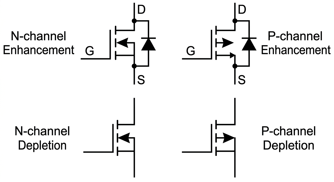
Figure 2: Standard schematic symbols for the four primary types of MOSFETs. Note the dashed channel lines for enhancement mode (normally-off) and solid lines for depletion mode (normally-on).
Enhancement-mode devices are by far the most common, because a normally-off switch is the safe and intuitive default for most designs. Depletion-mode parts, which conduct until you actively turn them off, show up in more specialised analog circuits.
The N-channel versus P-channel choice often comes down to where the switch sits. An N-channel enhancement device is a natural fit on the low side, between the load and ground, where its source is near ground and the gate is easy to drive positive. A P-channel device simplifies high-side switching, between the supply and the load, because it can be turned on by pulling the gate below the supply rail. N-channel parts generally offer better conduction for a given die area, so many high-side designs still use an N-channel device paired with a gate driver that lifts the gate above the supply, trading drive complexity for conduction performance.
MOSFET as a Switch and as an Amplifier
The most common job for a power MOSFET is to act as a switch. In the off state the channel is non-conducting and blocks the voltage across drain and source; in the on state the channel becomes a low-resistance path, so the device behaves much like a closed contact with a small resistive drop. Two properties make it a good switch: a low on-resistance, which keeps conduction loss down while current flows, and fast switching, which keeps the device from lingering in the lossy in-between region as it turns on and off. Designers care about both because real switching power is lost both while conducting and during each transition.
A MOSFET does not only snap between off and fully on, though. In its linear (also called active or saturation) region, the channel current varies smoothly with gate voltage, and the device can amplify a signal or regulate current in an analog sense. This region is essential for amplifiers and linear regulators, but it is also where the part dissipates the most heat, because it is simultaneously carrying current and dropping voltage. That is why switching applications try to move through the linear region quickly, while linear applications must plan carefully for the heat the device will produce.
The Parameters That Decide a MOSFET
Choosing a MOSFET is mostly about matching a handful of parameters to the job, and understanding what each one trades against. The values themselves live in the datasheet; what matters here is what each parameter governs and why it pulls the design in a particular direction.
| Parameter | What it governs | Why it matters |
|---|---|---|
| Drain-source voltage rating | The maximum voltage the device can block when off | Must clear the supply plus switching overshoot and ringing with margin |
| On-resistance | The resistive drop and conduction loss while on | Lower on-resistance cuts conduction loss but usually raises gate charge and cost |
| Gate charge | How much charge the driver must move to switch the gate | Higher gate charge means slower switching or a stronger driver and more drive loss |
| Threshold voltage | The gate voltage at which the channel begins to form | Sets logic-level compatibility and how the gate must be driven |
| Safe operating area | The combined voltage, current, and time limits the device tolerates | Linear and pulsed operation can violate it even when each rating alone looks fine |
| Thermal resistance and package | How effectively heat leaves the die | Decides the heatsinking and board copper needed to stay within temperature limits |
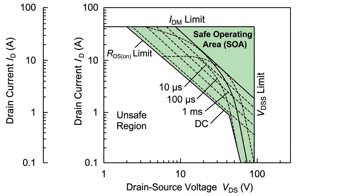
Figure 3: An example of a Safe Operating Area (SOA) plot. The operating point defined by drain-source voltage ($V_{DS}$) and drain current ($I_D$) must remain within these boundaries to avoid destroying the device.
The recurring theme is tension between conduction and switching. Pushing on-resistance down generally enlarges the die, which raises gate charge and slows switching unless the driver is made stronger. A part that is excellent for a slow, high-current load may be a poor fit for a fast switching converter, and vice versa. Picking a MOSFET well means deciding which of these losses dominates in your application before reading any single number.
How to Choose a MOSFET
A reliable selection flows in a sequence, starting with the limits that protect the part and ending with the refinements that optimise it. Working in this order keeps you from optimising a number that a later constraint would have overruled.
Set the voltage margin first. Establish the worst-case voltage the device must block when off, including switching overshoot and ringing, then require comfortable headroom above it before considering any other parameter.
Match the current and on-resistance to the conduction loss you can tolerate. Estimate the current the part will carry and how much resistive loss and heat that implies, and weigh it against the available cooling.
Check the gate charge against your driver and switching speed. Confirm the intended gate driver can move the gate charge fast enough for your switching frequency without excessive drive loss or slow, lossy transitions.
Verify the safe operating area for how the part is actually used. If the device spends time in the linear region, handles pulsed loads, or sees high voltage and current together, confirm those conditions sit inside the safe operating area, not just the individual maximum ratings.
Close on thermal behaviour and package. Choose a package and thermal path that hold the junction within its temperature limit under worst-case conditions, with the board copper or heatsink that implies.
This sequence is deliberately conservative: the voltage rating and safe operating area protect the device from outright destruction, so they come before the conduction and switching numbers that fine-tune efficiency. Treat the order as a checklist, and let the datasheet supply every actual figure.
Why MOSFETs Fail and How to Avoid It
Most MOSFET failures trace back to one of a few stresses that exceed what the part was rated to handle. Knowing the failure modes makes the selection checklist above feel less abstract, because each step is really guarding against one of these outcomes.
| Failure mode | Typical root cause | Practical guard |
|---|---|---|
| Overvoltage breakdown | Switching overshoot or ringing exceeding the voltage rating | Choose voltage margin generously and manage layout inductance and ringing |
| Thermal runaway / overtemperature | Conduction and switching loss outpacing the cooling path | Budget loss honestly and provide adequate heatsinking and copper |
| Safe-operating-area violation | High voltage and current together, or linear/pulsed stress | Verify operation against the safe operating area, not single ratings |
| Gate-oxide damage | Gate driven beyond its rated voltage, including transients and static | Respect the gate voltage limit and protect the gate from spikes and static |
| Slow or partial switching | Weak gate drive failing to move the gate charge promptly | Size the gate driver to the gate charge and switching speed needed |
Gate drive deserves special attention because it sits behind several of these modes at once. A gate driver that is too weak leaves the device dwelling in its lossy transition region, adding heat; a gate signal that overshoots can stress the thin oxide. Getting the gate voltage and drive strength right protects both the switching efficiency and the long-term survival of the part. When a design pushes any limit, a formal engineering review against the datasheet ratings is well worth the time before committing to a part.
Frequently Asked Questions
Is a MOSFET basically just a switch?
Acting as a switch is its most common job, where it turns fully on with low on-resistance and fully off to block voltage. It is more than a switch, though: in its linear region the channel conducts in proportion to the gate voltage, which lets the same device amplify signals or regulate current.
What are the four types of MOSFET?
The four come from two choices. Channel polarity gives N-channel or P-channel, and operating mode gives enhancement (normally off) or depletion (normally on). Combining them yields N-channel enhancement, P-channel enhancement, N-channel depletion, and P-channel depletion, with enhancement-mode parts being by far the most widely used.
How is a MOSFET different from a bipolar transistor?
A MOSFET is voltage-controlled through an insulated gate with high input impedance, so it needs almost no steady drive current once on. A bipolar transistor is current-controlled and needs continuous base current while it conducts. That difference is a major reason MOSFETs dominate switching power circuits.
When should I use N-channel versus P-channel?
An N-channel enhancement device suits low-side switching, where the source sits near ground and the gate is easy to drive positive. A P-channel device can simplify high-side switching, though many high-side designs still use an N-channel part with a gate driver that lifts the gate above the supply, because N-channel parts tend to conduct better for the same die area.
What usually causes a MOSFET to fail?
The common causes are overvoltage beyond the rating, overheating or thermal runaway, operating outside the safe operating area, gate-oxide damage from excessive gate voltage, and gate-drive that is too weak to switch the part cleanly. Selecting with margin and respecting the datasheet limits prevents most of these.
How do I start choosing a MOSFET for a project?
Begin with the worst-case blocking voltage and demand margin, then match current and on-resistance to the conduction loss and cooling you have, check that your gate driver can move the gate charge fast enough, verify the safe operating area for how the part is really used, and finish with package and thermal path. Read every actual number from the chosen part's datasheet.
Sources and References
Infineon MOSFET products and application notes confirm the structure of power MOSFETs and the role of voltage rating, on-resistance, and gate charge in selection, though the material is organised around Infineon's own portfolio, so the exact figures apply only to their parts.
onsemi MOSFET resources describe enhancement-mode operation and switching behaviour in a vendor-neutral enough way to learn the concepts, while the specific ratings naturally belong to the individual devices shown.
Texas Instruments power MOSFET overview is useful for the gate-drive and switching-loss relationships behind the gate-charge parameter, but it leans toward TI's driver and converter ecosystem rather than a neutral textbook treatment.
Vishay MOSFET product information is a good reference for how voltage rating, on-resistance, and package interact across a broad range of parts, with the caveat that you still need each part's datasheet for verified numbers.
Nexperia MOSFET pages explain N-channel and P-channel device behaviour and gate-drive requirements clearly, though they focus on Nexperia's catalogue and assume you will confirm details in the relevant datasheet.
Toshiba MOSFET product pages cover safe operating area and thermal considerations alongside switching roles, and like the others they describe their own devices rather than serving as an independent standard.
 UTMEL
UTMEL
We are the professional distributor of electronic components, providing a large variety of products to save you a lot of time, effort, and cost with our efficient self-customized service. careful order preparation fast delivery service
 MOSFET vs IGBT: Structure, Switching Behavior, and How to ChooseUTMEL21 September 202624576
With the rise of new energy in recent years, the market demand for MOSFETs and IGBTs is increasing steeply. Generally used as switching devices, they are widely used in electronic circuits. MOSFETs and IGBTs are relatively similar in appearance and characteristics parameters. So what is the difference between MOSFETs and IGBTs?
Read More Introduction to FinFETUTMEL18 March 202131320
The full name of FinFET is Fin Field-Effect Transistor. It is a new complementary metal oxide semiconductor transistor. The FinFET name is based on the similarity between the shape of the transistor and the fin.
Read More What Is a MOSFET? Working Principle, Types, and Selection GuideUTMEL15 July 20268149
This guide walks through how a MOSFET works, how it differs from an ordinary bipolar transistor, the four standard types, the roles it plays in a circuit, and a practical, parameter-driven way to choose one. Because this topic invites a lot of numbers, the discussion stays qualitative on purpose. Any exact voltage, resistance, current, or thermal figure belongs to the specific part you are using, so treat the manufacturer datasheet as the final word on every number.
Read More NPN Transistors and PNP TransistorsUTMEL29 October 202010160
NPN and PNP are two types of transistors. Transistors are semiconductor devices made of doped p-type and n-type junctions. This article mainly introduces the differences between this two kinds of transistors, the methods of distinguishing them, and the application of them.
Read More An Overview of Bipolar TransistorsUTMEL27 August 20209422
Bipolar Transistor, full name bipolar junction transistor(BJT), is an electronic device with three terminals, made of three parts of semiconductors with different levels of doping. The charge flow in the transistor is mainly due to the diffusion and drift movement of carriers at the PN junction.
Read More
Subscribe to Utmel !
![BLM18PG330SN1D]() BLM18PG330SN1D
BLM18PG330SN1DMurata Electronics
![ENW-89847A3KF]() ENW-89847A3KF
ENW-89847A3KFPanasonic Electronic Components
![BLM03AX102SN1D]() BLM03AX102SN1D
BLM03AX102SN1DMurata Electronics
![TP88]() TP88
TP88Fluke Electronics
![1212039]() 1212039
1212039Phoenix Contact
![BLM15AG121SN1D]() BLM15AG121SN1D
BLM15AG121SN1DMurata Electronics
![01050003H]() 01050003H
01050003HLittelfuse Inc.
![7BB-12-9]() 7BB-12-9
7BB-12-9Murata Electronics
![7BB-20-6L0]() 7BB-20-6L0
7BB-20-6L0Murata Electronics
![PKMCS1818E20A0-R1]() PKMCS1818E20A0-R1
PKMCS1818E20A0-R1Murata Electronics


