Product
 Brand
Brand Articles
 Tools
Tools
How to Select a Current Sense Amplifier for Power Monitoring: An Engineering Selection & Error Budget Guide
The direct answer: current sense amplifier selection for power monitoring reduces to matching the amplifier's input common-mode range, offset voltage, gain accuracy, and bandwidth against the electrical signature of the power rail you are measuring. Start by defining the bus common-mode voltage, minimum and maximum load currents, required fault-response latency, and directionality. Then eliminate topologies that cannot survive your rail transients. Finally, build a DC and thermal error budget to verify that the selected amplifier plus shunt resistor combination meets your accuracy target across the full operating temperature range.
This guide walks through the selection workflow in the order a hardware designer should actually execute it: topology choice first, silicon parameters second, error budgeting third, and PCB-level validation last.
Structured Decision Aid: Power Rail Architecture Selection Matrix
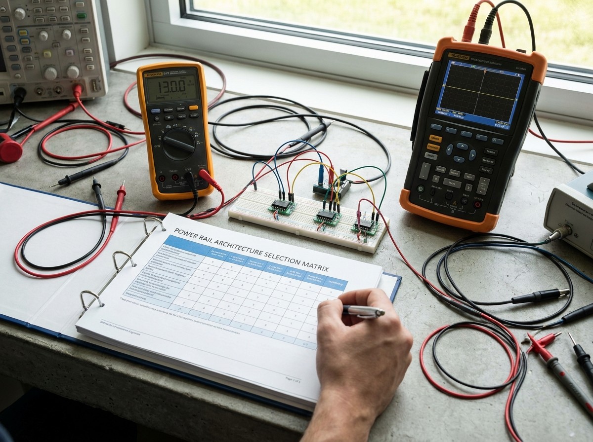
Match your rail to the sensing architecture and silicon type before comparing individual part numbers.
| Power Rail Category | Typical Bus Voltage | Optimal Topology | Recommended CSA Silicon Type | Primary Design Constraint |
|---|---|---|---|---|
| Low-Voltage Digital Core | 0.8 V – 1.8 V | High-Side | Low-VOS precision analog CSA or PMBus monitor | Sub-milliohm shunt dissipation and light-load VOS error |
| Standard 12 V / 24 V Industrial Rail | 12 V – 24 V | High-Side | Dedicated wide-VCM analog CSA | Rail transient tolerance and VCM > VCC capability |
| 48 V Telecom / Server Distribution | 48 V | High-Side | 80 V+ high-voltage CSA or isolated monitor | High-voltage breakdown and surge margin |
| Battery Management Systems | 12 V – 60 V | High-Side or Low-Side | Bidirectional CSA with VREF biasing | Symmetric charge/discharge sensing and sleep-mode IQ |
| PWM Motor Phase / In-Line Inverter | 0 V – VBUS switching | In-Line | High AC-CMRR / enhanced PWM-rejection CSA | Fast dV/dt switching transient immunity |
This table is a starting point, not a replacement for the error budget. The sections below explain the reasoning behind each mapping and the conditions under which you should override it.
Current Sensing Topologies: High-Side, Low-Side, and In-Line Trade-Offs
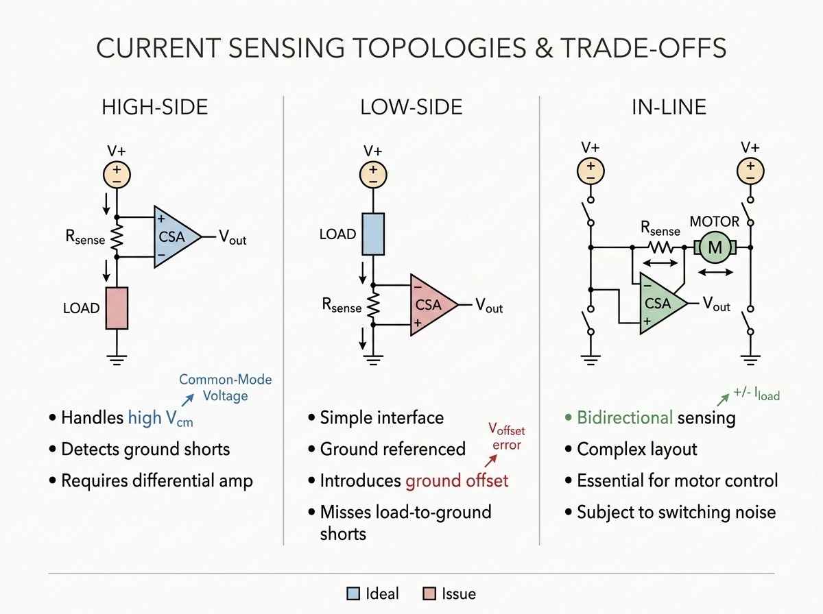
The physical placement of the shunt resistor determines the common-mode voltage the amplifier must tolerate, the integrity of the system ground reference, and the types of faults the circuit can detect.
High-Side Sensing
The sense resistor sits between the supply rail (VBUS) and the load. Current flowing into the load produces a small differential voltage across the shunt, riding on top of the full bus voltage.
High-side sensing simultaneously delivers two benefits that make it the default choice for power monitoring in most systems. First, it directly detects load short-to-ground faults: any fault current that flows from the rail through the load to ground must pass through the shunt first, producing an unmistakable differential signature. Second, it leaves the system ground reference untouched. There is no ground elevation, no ground-loop injection, and no disruption to analog references or digital communication signals such as I2C logic-low thresholds.
The reason high-side sensing once posed a practical barrier is that the amplifier's input common-mode range must cover the bus voltage itself. Many high-side rails run at 12 V, 24 V, or 48 V, while the control circuitry that reads the current output may run on a 3.3 V or 5 V supply. Dedicated current sense amplifiers[1] solve this with internal level-shifting architectures that allow the input common-mode voltage to exceed the amplifier supply voltage (VCM > VCC) — often by an order of magnitude or more. According to Texas Instruments' application documentation, this capability is the defining architectural difference between dedicated CSAs and general-purpose op-amps or instrumentation amplifiers.
Who should avoid high-side sensing: Designs where the bus voltage is so low that a standard op-amp or even a microcontroller ADC can read the shunt voltage directly, and where the added cost of a dedicated high-side CSA cannot be justified. In such cases, low-side sensing may be acceptable.
Low-Side Sensing
The sense resistor sits between the load and system ground. The shunt voltage is referenced to ground, so the common-mode voltage stays near 0 V. That makes low-side sensing electrically convenient: standard single-supply operational amplifiers, low-voltage CSAs, or even a microcontroller's integrated ADC can often read the signal directly.
The hidden penalty is ground elevation. Because the load current passes through the shunt before returning to ground, the load's "ground" potential is lifted by VGND_LIFT = ILOAD × RSHUNT. For a 10 A load through a 1 milliohm shunt, this is only 10 millivolts — but that 10 millivolts appears in series with every analog reference and digital communication return path. It can shift I2C logic-low thresholds, corrupt ADC ground references, and create ground noise that analog circuits interpret as genuine signal. Low-side sensing is also blind to short-to-ground faults at the load, since the fault current bypasses the shunt and flows directly from the supply rail into the ground plane.
Low-side sensing is a legitimate cost-optimization approach when the load current is modest, the shunt resistance is small, and the system is not sensitive to ground elevation. It is not a general-purpose substitute for high-side sensing in power monitoring.
In-Line (Phase) Sensing
The sense resistor sits directly in a switching phase path — for example, in series with a brushless motor phase lead or a synchronous buck converter's output inductor. This topology measures the actual phase current flowing through the load, which is what the motor controller or current-mode control loop needs.
The challenge is that the common-mode voltage at the shunt does not sit at a fixed level. It transitions between approximately 0 V and the full bus voltage at the switching frequency, with extremely fast dV/dt slew rates. The amplifier sees a square-wave common-mode input with high-frequency harmonics well beyond the switching fundamental. Standard DC common-mode rejection specifications provide no guarantee of accurate operation under these conditions. Specialized PWM-rejection amplifiers are designed to reject these fast common-mode transients and settle quickly after each edge.
High-Side vs. Low-Side vs. In-Line Comparison
| Evaluation Criterion | High-Side Sensing | Low-Side Sensing | In-Line (Phase) Sensing |
|---|---|---|---|
| Shunt Placement | Between supply rail and load | Between load and ground | Directly in switching phase path |
| Input VCM Potential | VBUS (may exceed VCC) | Near 0 V | 0 V to VBUS square-wave switching |
| Ground Reference Integrity | Uninterrupted ground plane | Ground elevation (ILOAD × RSHUNT) | Uninterrupted ground plane |
| Short-to-Ground Detection | Directly detectable | Not detectable | Partially detectable, phase-dependent |
| Component Complexity | Requires dedicated high-VCM CSA | Standard op-amp or low-voltage CSA usable | Requires PWM-rejection / high AC-CMRR CSA |
| Sensitivity to Switching Transients | Moderate, rail-dependent | Low | Severe — dV/dt rejection mandatory |
| Best For | Power monitoring, fault detection, battery management | Cost-sensitive low-current monitoring | Motor phase currents, current-mode control |
Why answers sometimes disagree on topology: vendor application notes from TI, Analog Devices, and STMicroelectronics all converge on high-side sensing as the recommended default for power monitoring, but they differ in emphasis. Low-side sensing advocates tend to prioritize BOM cost and design simplicity; high-side advocates prioritize fault coverage and ground integrity. Both positions are technically correct within their implicit constraints. The disagreement disappears once you specify whether fault detection and ground-reference integrity are non-negotiable requirements.
Core Electrical Specifications to Compare: Beyond the Datasheet Headline
Once you have chosen a topology, the datasheet comparison begins. Most selection mistakes occur when a designer compares only the headline bandwidth or gain specification and misses the parameters that actually dominate measurement accuracy.
Input Common-Mode Voltage Range: Operating vs. Survival Limits
Every CSA datasheet specifies two common-mode voltage ranges. The linear operating VCM range is the domain in which the datasheet's electrical performance specifications hold: offset voltage, gain accuracy, CMRR, and linearity. The absolute maximum survival rating is the domain in which the device will not be permanently damaged, but within which parametric performance is not guaranteed.
When sizing the amplifier, use the linear operating range for accuracy budgeting and the survival rating for fault tolerance. Inductive kickback, load-dump transients, and reverse-battery events can temporarily push the bus voltage far beyond normal operation. The amplifier must survive these excursions without permanent damage, but you should not expect the measurement to remain accurate during the transient unless the linear range also covers it.
Input Offset Voltage and Thermal Drift
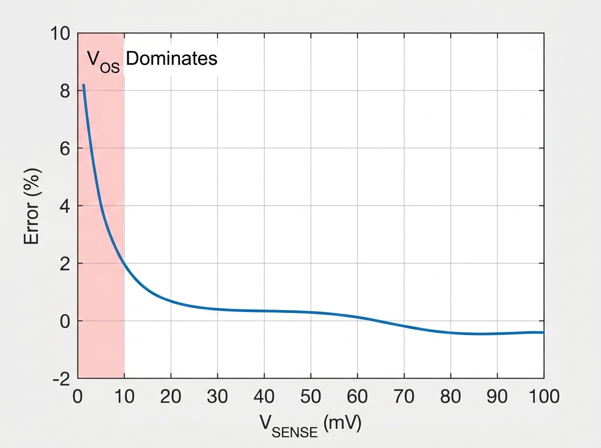
Input offset voltage (VOS) is the single most mis-ranked parameter in CSA selection because its impact is dynamic-range-dependent, not fixed. The offset error percentage is:
At full-scale current, where VSENSE is largest (typically 50 mV to 100 mV), a 100 microvolt offset contributes only 0.1% to 0.2% error. At minimum load, where VSENSE may drop to 1 mV or below, the same offset contributes 10% or more. Offset voltage is therefore the primary accuracy limiter at the bottom of the dynamic range — exactly where load monitoring often needs to detect standby current, sleep modes, or leaky subsystems.
Thermal drift amplifies this problem across temperature. Zero-drift / chopper-stabilized current sense amplifiers, such as the TI INA240 or ST TSC240 lines, achieve input offset voltages as low as ±20 µV to ±25 µV maximum with thermal drift in the 150 nV/°C to 250 nV/°C range. This level of offset stability enables accurate current measurement with full-scale shunt voltage drops down to 10 mV across −40 °C to +125 °C, according to the respective manufacturer datasheets. If your minimum load current would produce a shunt voltage below roughly 10 times the amplifier's VOS maximum, you should either increase the shunt resistance, select a lower-offset amplifier, or accept degraded low-end accuracy.
Common-Mode Rejection Ratio: DC vs. High-Frequency AC Roll-Off
CMRR expresses the amplifier's ability to reject changes in the input common-mode voltage. In high-side sensing, the bus voltage is the common-mode voltage. If the bus voltage shifts — due to load transients, battery discharge, or switching noise — an amplifier with inadequate CMRR will produce an output change that looks indistinguishable from a genuine current change.
The DC CMRR specification is measured at low frequency and is the number most often quoted. It tells you nothing about performance at switching frequencies. Many amplifiers with excellent DC CMRR (over 100 dB) experience severe CMRR degradation as the common-mode input frequency rises. In any system where the bus rail carries switching converter noise or the sensing node experiences dV/dt transients, the AC CMRR characteristic matters as much as or more than the DC value.
Discrete difference amplifier math callout: A standard resistor-network difference amplifier built with discrete 1% resistors has a worst-case CMRR of only 36 dB to 40 dB, limited by resistor matching. That translates to roughly 20 mV of output error per 1 V of common-mode voltage change, per Analog Devices' technical documentation[2] and TI's SBOA374 application note[5]. Dedicated CSAs with on-chip laser-trimmed resistor networks achieve DC CMRR specifications in the 100 dB to 132 dB range because their internal resistors are matched to 0.01% or better. This is not a small difference — it is a 60 dB to 90 dB gap in a parameter where error scales directly with bus voltage variation.
Gain Staging and Integrated Resistor Matching
Fixed-gain CSAs (common values: 20, 50, 100, 200 V/V) integrate the gain-setting resistor network on-chip. This eliminates the external resistor matching problem entirely and is the primary reason dedicated CSAs achieve high CMRR ratings. Select the gain so that the full-scale output voltage stays within the input range of the downstream ADC while leaving margin for overcurrent transients.
The full-scale mapping is:
A practical target is to use 80% to 90% of the ADC's full-scale input span at rated maximum current. This reserves headroom for dynamic overcurrent transients while maximizing available dynamic range. Avoid selecting a gain so large that the amplifier output saturates at the high rail (VOH) before the ADC reaches full scale, and avoid a gain so small that minimum-load signals remain buried in offset noise.
Directionality and Reference Biasing
Unidirectional sensing measures current flowing in a single direction. At zero current, the output sits at the amplifier's lowest output voltage (VOL — more on this later). This architecture maximizes dynamic range for single-polarity rails: power supplies, LED drivers, downstream DC-DC converters.
Bidirectional sensing measures current in both directions, such as charging and discharging currents in a battery management system or regenerative braking current in a motor drive. The zero-current output is not 0 V; it is level-shifted to a reference voltage, typically VCC/2 or a user-provided external reference. This shifts the zero point to mid-scale, allowing the output to swing above and below the reference to represent positive and negative currents respectively. The zero-current output level is:
Directionality is a fundamental architectural choice, not a component parameter to optimize later. It affects the entire output signal chain, the ADC interpretation software, and the comparator trip thresholds.
Bandwidth, Slew Rate, and Settling Time
Bandwidth determines the fastest current waveform that can be faithfully reproduced. Slew rate determines the maximum rate of change the output can follow, and settling time determines how quickly the output recovers after a step transient.
For power monitoring telemetry, bandwidth requirements are typically modest — tens of kilohertz is often sufficient to track load-drawn DC and low-frequency load changes. For overcurrent protection, the requirements are much more demanding. A fast analog CSA can respond in under 1 microsecond, making it suitable for hardware overcurrent protection loops that must trip before excessive current damages downstream components. This latency contrast is the primary driver of the analog-versus-digital architectural decision detailed later in this guide.
Mathematical DC and Thermal Error Budgeting: Worst-Case vs. RSS
A rigorous DC error budget tells you whether the selected amplifier and shunt resistor can meet your accuracy target at both ends of the dynamic range. It also reveals which error terms dominate, directing your optimization effort where it will have the most impact.
Component Error Formulations
Each error source contributes input-referred error voltage. Expressed as a percentage of the shunt voltage at any given load current, the individual contributions are:
Input offset voltage error:
Amplifier gain error:
Common-mode rejection error:
Power supply rejection error:
Shunt resistor tolerance and thermal drift:
Where TCR is expressed in parts per million per degree Celsius and ΔT is the temperature rise above the reference temperature, in degrees Celsius.
Statistical vs. Deterministic Error Modeling
Two summation methodologies provide different views of the total error.
Worst-Case Summation adds all error terms linearly:
This calculates the absolute theoretical maximum error assuming every error source simultaneously reaches its worst-case limit in the same direction. It is conservative and suitable for safety-critical systems where the measurement must be guaranteed to fall within a defined band under all conditions.
Root-Sum-Square (RSS) Summation combines the terms geometrically:
The RSS method assumes that error sources are statistically independent and normally distributed, which yields a more realistic estimate of typical performance. The method is validated in Analog Devices' DC error budget methodology[3] and Renesas AN1298[6]. RSS does not guarantee the absolute worst-case boundary; it represents a statistical expectation. When certifying designs to formal accuracy limits, use worst-case summation. When optimizing a design for typical manufacturing yield, RSS is the more practical metric.
Worked Engineering Example: 12 V Rail with 10 A Nominal, 100 mA Minimum
Use the following representative datasheet values to illustrate the methodology only. These values are illustrative placeholders, not from a single datasheet, and do not represent the performance of any specific current sense amplifier or shunt resistor. Always substitute the actual datasheet limits for the specific part you evaluate.
Setup parameters:
| Parameter | Value | Notes |
|---|---|---|
| Bus voltage (VBUS) | 12 V | High-side sensing |
| Nominal full-scale current (IMAX) | 10 A | Continuous rating |
| Minimum monitored current (IMIN) | 100 mA | Standby leakage target |
| Shunt resistor (RSHUNT) | 10 mΩ | 1 W dissipation at 10 A |
| Amplifier VOS (representative) | 100 µV | Standard precision CSA |
| Gain error (representative) | 0.3% | Datasheet specification |
| CMRR (DC, representative) | 100 dB | DC specification |
| ΔVCM assumed | 1 V | Bus transient amplitude |
| PSRR (representative) | 80 dB | DC specification |
| ΔVSUPPLY assumed | 0.1 V | Supply ripple amplitude |
| Shunt initial tolerance | 0.5% | Precision surface-mount |
| Shunt TCR | 50 ppm/°C | Precision resistor grade |
| ΔT (shunt self-heating + ambient) | 50 °C | Worst-case temp rise |
Error contributions at full-scale (10 A, VSENSE = 100 mV):
| Error Source | Calculation | Contribution |
|---|---|---|
| VOS | (100 µV / 100 mV) × 100 | 0.10% |
| Gain Error | From datasheet | 0.30% |
| CMRR Error | (1 V × 10⁻⁵ / 100 mV) × 100 | 0.01% |
| PSRR Error | (0.1 V × 10⁻⁴ / 100 mV) × 100 | 0.01% |
| Shunt Error | 0.5% + (50 × 10⁻⁴ × 50) | 0.75% |
Full-scale total error: Worst-Case ≈ 1.17%. RSS ≈ 0.81%. At full-scale, gain error and shunt resistor tolerance dominate. Optimizing VOS will barely move the needle here.
Error contributions at light-load (100 mA, VSENSE = 1 mV):
| Error Source | Calculation | Contribution |
|---|---|---|
| VOS | (100 µV / 1 mV) × 100 | 10.00% |
| Gain Error | From datasheet | 0.30% |
| CMRR Error | (1 V × 10⁻⁵ / 1 mV) × 100 | 1.00% |
| PSRR Error | (0.1 V × 10⁻⁴ / 1 mV) × 100 | 1.00% |
| Shunt Error | 0.5% + (50 × 10⁻⁴ × 50) | 0.75% |
Light-load total error: Worst-Case ≈ 13.05%. RSS ≈ 10.13%. At minimum load, input offset voltage dominates by an order of magnitude over every other error source combined. This is the single most important insight from the error budget: if you need tight accuracy across a wide dynamic range, your VOS budget at IMIN — not at IMAX — determines the amplifier selection.
The worked example uses representative values for illustration. Always substitute the actual datasheet limits for the specific part you evaluate, and re-run the budget at both the minimum and maximum temperature corners.
Architectural Choice: Discrete Analog CSAs vs. Integrated Digital Power Monitors
Once the error budget validates the topology and shunt choice, the next architectural decision is whether the current measurement should be delivered as an analog voltage signal or as a digital bus telemetry stream.
Analog Current Sense Amplifiers
An analog CSA outputs a continuous voltage proportional to the sensed shunt current: VOUT = Gain × VSENSE + VREF. The output is immediate, continuous, and free of bus communication latency. This makes analog CSAs the right choice when the current signal must drive hardware-level decision making — an analog comparator for overcurrent trip, a PWM controller's current-mode feedback pin, or a motor control loop's torque input.
Best for: Hardware overcurrent protection with sub-microsecond response, real-time current-mode control loops, motor torque feedback, and any application where the current signal must be processed in the analog domain before a microcontroller can sample and react.
Who should avoid analog CSAs: Systems whose primary need is digital power telemetry reporting to a host controller, where the bus current and voltage must be converted to power readings, energy accumulation, or fault registers over a multi-drop communication bus. Adding a discrete ADC and performing the power math in the MCU may consume more processor cycles and board space than an integrated digital monitor.
Digital Power Monitors
A digital power monitor integrates the CSA front-end with an ADC, precision voltage reference, digital multiplier, and a serial interface (I2C, SMBus, SPI, or PMBus). It measures bus voltage and shunt current internally, calculates active power (P = V × I) and energy accumulation (E = ∫P dt), and reports the results over the digital bus. Integrated digital power monitors such as the TI INA228 feature up to 20-bit delta-sigma ADCs, input bias currents down to approximately 2.5 nanoamperes, common-mode capability up to 85 V, and digital alert propagation latencies around 75 microseconds, per TI and Analog Devices documentation. This latency is far too slow for direct hardware overcurrent intervention but entirely adequate for system telemetry polling.
Best for: Server rack power monitoring, telecommunications power distribution, battery charging telemetry, system-level health diagnostics, and any application where the host controller is better served by reading ready-made digital power values off a bus than by sampling and processing analog signals itself.
Who should avoid digital monitors: Closed-loop control applications where the current signal must directly modulate a PWM duty cycle or trigger an analog comparator in under a microsecond. The ADC conversion time and bus arbitration latency introduce a delay that can be fatal to a power stage during a hard short-circuit.
Analog vs. Digital Comparison Matrix
| Parameter | Analog CSA | Digital Power Monitor |
|---|---|---|
| Output Signal | Continuous analog voltage | Digital bus data (I2C/SPI/PMBus) |
| Control Loop Latency | Sub-microsecond (< 1 µs typical) | ~75 µs to milliseconds (per digital alert specs) |
| Telemetry Capability | Current only (proportional voltage) | Voltage, current, power, energy accumulation |
| Host Controller Overhead | Requires ADC sampling and power math | Minimal — data arrives pre-computed |
| External ADC Requirement | Required for digital systems | Not required — integrated |
| Hardware Fault Trip Capability | Directly drives analog comparator | Usually requires software polling or configured alert pin |
| Typical Applications | OCP, current-mode control, torque feedback | Server PMBus, telemetry, energy monitoring |
The Hybrid Architecture Approach
The most robust power monitoring designs combine both paths. A fast analog CSA monitors the shunt and feeds a hardware comparator whose output directly drives a shutdown or current-limit pin. In parallel, a digital power monitor on the same shunt reports voltage, current, and power telemetry to the host controller for logging, throttling decisions, and power budgeting. This hybrid approach eliminates the false choice between fast fault protection and rich telemetry — get both by architecting two separate measurement paths with different latency budgets.
Shunt Resistor Sizing, Thermal Management, and 4-Wire Kelvin PCB Layout Rules
The shunt resistor and the amplifier form a single measurement system. Selecting the shunt resistor incorrectly or routing the PCB without considering parasitic resistance can negate every benefit of a well-chosen CSA.
Shunt Resistor Sizing Trade-Off
The shunt resistance is constrained from two directions. From above, it must be low enough that the power dissipation at full-scale current stays within the resistor's thermal rating:
From below, it must be high enough that the sense voltage at minimum current stays above the amplifier's input offset voltage by a meaningful margin:
These two constraints pull in opposite directions. A larger resistance improves signal-to-noise ratio at light load but increases thermal dissipation and voltage drop at full scale. A smaller resistance reduces heat and voltage loss but degrades low-end accuracy because the sense voltage shrinks toward the amplifier's offset voltage floor.
A practical design approach: start with a target full-scale sense voltage (commonly 50 mV to 100 mV for power monitoring, or as low as 10 mV for high-current, low-loss applications using precision zero-drift amplifiers). Solve for the shunt resistance, then verify that the resulting light-load sense voltage provides an acceptable offset error percentage, and check the thermal dissipation against the resistor's power rating with at least 50% derating.
The Physics of 4-Terminal Kelvin Sensing
For shunt values in the milliohm to sub-milliohm range, the resistance contributed by the PCB traces and solder joints connecting the shunt to the amplifier becomes a first-order error source. A standard 1 oz copper PCB trace has approximately 0.5 milliohm of resistance per square. An uncompensated 1 millimeter to 2
Sources and references used for this guide
Current-sense amplifiers | TI.com
Source type: official company documentation
Used for: Core selection criteria, high-side vs low-side sensing parameters, and bus voltage capabilities.
Caution: Vendor product catalog; focus on parametric principles rather than specific proprietary part numbers.High-Side Current-Sense Measurement: Circuits and Principles
Source type: official company documentation
Used for: High-side sensing circuit topologies, difference amplifier comparison, and common-mode rejection requirements.
Caution: Vendor technical article; verify generalized circuit math against standard op-amp theory.DC Error Budget Calculator Simplifies Selection of Optimal Current-Sense Amplifiers
Source type: official company documentation
Used for: DC error budget calculation methodology, RSS vs Worst-Case error formulas, Vos, and gain error analysis.
Caution: Vendor technical article; equations apply universally to shunt-based measurement but verify notation.How to choose the right current sense amplifier for your design
Source type: official company documentation
Used for: Input common-mode voltage selection, load current dynamic range, and bidirectional sensing requirements.
Caution: Vendor learning portal; provides high-level architectural guidance.Difference Between an Instrumentation Amplifier and a Current Sense Amplifier
Source type: official company documentation
Used for: Architectural comparison between difference amplifiers, in-amps, and dedicated current sense amplifiers.
Caution: Vendor application note; specifically addresses high common-mode voltage advantages of dedicated CSAs.AN1298: Instrumentation Amplifier Application Note
Source type: official company documentation
Used for: Error budget summation methodology and input-referred error factor analysis.
Caution: Application note covers instrumentation amplifiers; principles apply directly to differential sensing error stacks.High-Side Current Sensing: Difference Amplifier vs. Current-Sense Amplifier
Source type: reputable professional source
Used for: Discrete resistor mismatch mathematical analysis and CMRR degradation in discrete difference amplifiers.
Caution: Technical paper by H. Sino; provides excellent circuit derivations for resistor tolerance effects.Monitoring Power with Current Sense Amplifiers
Source type: reputable professional source
Used for: Trade-offs between shunt resistor accuracy, power dissipation, and amplifier dynamic range.
Caution: Distributor engineering overview; use for high-level power management framing.
 UTMEL
UTMEL
We are the professional distributor of electronic components, providing a large variety of products to save you a lot of time, effort, and cost with our efficient self-customized service. careful order preparation fast delivery service
 Introduction to MD8002A Audio AmplifierUTMEL27 March 20259696
The MD8002A is an audio power amplifier that uses a 5V DC power supply to provide 2.0 watts of continuous power to a BTL load with less than 10% distortion. It was created with the aim of providing high-quality o/p control with fewer components. It doesn't use any output coupling capacitors or bootstrap capacitors.
Read More Understanding the Low Noise Amplifier (LNA)UTMEL20 March 202526384
A low noise amplifier is an amplifier with a very low noise figure. It is generally used as a high-frequency or intermediate-frequency preamplifier for various types of radio receivers, as well as amplifying circuits for high-sensitivity electronic detection equipment.
Read More Introduction to Optical AmplifierUTMEL27 March 202510367
An optical amplifier is a subsystem product that can amplify optical signals in optical fiber communication systems. The principle of the optical amplifier is basically based on the stimulated radiation of the laser, which realizes the amplification effect by converting the energy of the pump light into the energy of the signal light.
Read More What is an Inverting Amplifier?UTMEL25 April 202512274
An inverting amplifier is a fundamental configuration of operational amplifiers where the output signal has opposite polarity to the input signal. This configuration uses an operational amplifier with its inverting input terminal receiving the input signal, while the non-inverting terminal is typically connected to ground. The primary function of this circuit is to amplify the input signal while inverting its phase by 180 degrees.
Read More Low-Power Design of Operational AmplifiersUTMEL27 March 20257622
Hello, this is Candy. With the rise in popularity of battery-powered electronics in recent years, analog circuit designers have been increasingly concerned about power usage. This article will cover how to use low-power op amps in system design, as well as low-power op amps with low supply voltage capabilities and their applications, as well as how to read and understand op amp data sheets appropriately. Circuit design with energy-saving technologies for more efficient device choices.
Read More
Subscribe to Utmel !
![JANTX1N6037A/TR]() JANTX1N6037A/TR
JANTX1N6037A/TRMicrochip Technology
![LTC4368HMS-1#PBF]() LTC4368HMS-1#PBF
LTC4368HMS-1#PBFLinear Technology/Analog Devices
![TBU-CA025-050-WH]() TBU-CA025-050-WH
TBU-CA025-050-WHBourns Inc.
![01550900M]() 01550900M
01550900MLittelfuse Inc.
![SN65240PWRG4]() SN65240PWRG4
SN65240PWRG4Texas Instruments
![LT4363MPS-1#PBF]() LT4363MPS-1#PBF
LT4363MPS-1#PBFLinear Technology/Analog Devices
![M15KP30CA/TR]() M15KP30CA/TR
M15KP30CA/TRMicrochip Technology
![TPD13S523RSVR]() TPD13S523RSVR
TPD13S523RSVRTexas Instruments
![1N5665A/TR]() 1N5665A/TR
1N5665A/TRMicrochip Technology
![P40-G240-WH]() P40-G240-WH
P40-G240-WHBourns Inc.