

 Product
 Brand
 Articles
 Tools

Reverse-Polarity Protection for DC Inputs: Diode and MOSFET Trade-Offs
A reverse polarity protection circuit prevents catastrophic component damage when a DC power supply, battery lead, or field wiring terminal is connected backward. For low-current inputs, a series diode offers single-component simplicity but introduces a continuous forward voltage drop () and linear heat loss (). For higher-current or tight-headroom rails, a high-side P-channel MOSFET shunts its intrinsic body diode once enhanced, reducing conduction loss towhen wired with its Drain facing the input.
Executive Triage for Designers and Repair Engineers:
Need to select a topology quickly? Jump to the Quick Decision Framework and Master Comparison Table to match your current budget and voltage headroom against four standard protection schemes.
Verifying a P-MOSFET schematic? Review the Drain-vs-Source Orientation Trap to ensure the intrinsic body diode blocks reverse polarity rather than conducting fault current into the load.
Debugging a dead board or signing off a PCB layout? Use the Component Selection and Bench Verification Checklist to audit absolute maximum ratings (,,) and gate-clamping networks.
Quick Decision Framework: Choosing Between a Series Diode and a High-Side P-MOSFET
Selecting between a series diode and a high-side P-channel MOSFET hinges on load current, allowable rail voltage drop (versus), PCB thermal limits, and input voltage range relative to MOSFET gate ratings. According to design guidance from Monolithic Power Systems (MPS), series diodes are typically confined to low-current applications up to roughly 2 A to 3 A[4], whereas high-side P-MOSFETs minimize insertion loss in higher-current or tight-headroom designs.
Before placing parts on a schematic, evaluate four circuit variables against your system requirements:
Minimum Input Voltage Headroom: Can downstream low-dropout regulators (LDOs) or DC-DC buck converters tolerate a permanent diode forward voltage drop () when the input battery or supply is at its lowest operating voltage?
Continuous and Peak Load Current (): Does linear diode heating () exceed your enclosure and PCB copper thermal budget? While MPS notes 2 A to 3 A as a typical ceiling for series diodes, the exact boundary depends on ambient temperature, package thermal resistance (), and available copper pour area.
Input Voltage Range vs. Gate Oxide Limits: Does the maximum input voltage () plus line transients exceed the MOSFET's absolute maximum gate-to-source rating ()? Conversely, does the minimum input voltage () fall too close to the MOSFET gate threshold voltage () to fully enhance the channel?
Static Miswiring vs. Dynamic Back-Feeding: Is the input stage only guarding against a technician connecting power leads backward (static reverse polarity), or must it also block reverse current from flowing backward out of a charged output capacitor or battery into a sagging input rail?
Master Topology Comparison Table
Application notes from onsemi (AND90146-D), Texas Instruments (SLVA139), Allegro MicroSystems (P0236), and Monolithic Power Systems divide DC reverse-polarity protection into passive junction blocking, self-biased MOSFET switches, and active controller architectures:
| Protection Topology | Blocking Mechanism | Forward Voltage Drop | Conduction Power Loss | Startup Behavior | Reverse-Current / Back-Feed Blocking | Relative BOM Complexity | Typical Application Tier |
|---|---|---|---|---|---|---|---|
| Series Silicon PN Diode | Reverse-biased PN junction | High (of silicon junction; verify in datasheet) | Instant passive conduction when | Blocks both static reverse polarity and dynamic backflow | Lowest (1 component) | Low-current rails with wide voltage headroom and high reverse-voltage spikes | |
| Series Schottky Diode | Reverse-biased metal-semiconductor barrier | Moderate (lowerthan PN diode; verify in datasheet) | (in reverse bias) | Instant passive conduction when | Blocks backflow, but exhibits high thermal reverse leakage () | Lowest (1 component) | Low-current rails (typically up to 2 A–3 A per MPS) needing lower drop than PN diodes |
| High-Side P-Channel MOSFET (Self-Biased) | Reverse-biased intrinsic body diode with channel off | Very low () | Conducts via body diode first, then enhances channel once | Does not block dynamic backflow while output rail holds Source positive | Moderate (MOSFET + Zener clamp + resistor) | Low-headroom and medium-current DC inputs requiring low insertion loss | |
| High-Side N-Channel MOSFET + Ideal-Diode Controller | Active comparator turns gate off; body diode blocks | Ultra-low () | + IC quiescent power | Body diode conducts briefly until charge pump drives gate above Source | Actively senses and blocks reverse current / input brownouts | Highest (N-MOSFET + controller IC + passives) | High-current rails, redundant power OR-ing, and capacitive/battery hold-up loads |
Option-by-Option Engineering Breakdown
Series Silicon PN Diode
Best for: Auxiliary control inputs, low-current sensor power rails, and harsh industrial environments with high reverse-voltage transients.
Core strength: High repetitive peak reverse voltage () ratings and negligible reverse leakage current across temperature.
Primary drawback: Highest forward voltage drop (), which wastes power as heat and reduces downstream regulator headroom.
Series Schottky Diode
Best for: Cost-sensitive DC inputs (typically up to the 2 A to 3 A range noted by MPS) where a standard silicon PN junction drops too much voltage.
Core strength: Lower forward voltage drop than a standard silicon rectifier with single-component layout simplicity.
Primary drawback: Lower reverse-bias breakdown voltage () and exponentially increasing reverse leakage current () at high ambient temperatures.
High-Side P-Channel MOSFET (Self-Biased)
Best for: Battery-powered equipment, automotive electronic control units (ECUs), and DC barrel/screw-terminal inputs where diode heat or voltage loss is unacceptable.
Core strength: Replaces fixed junction voltage drop with scalable channel resistance () without disrupting the system ground return path.
Primary drawback: Requires a Zener diode and resistor network to protect the gate on higher-voltage rails, and allows bidirectional current flow once enhanced—meaning it cannot stop a charged output capacitor from back-feeding a shorted input.
High-Side N-Channel MOSFET + Ideal-Diode Controller
Best for: High-current power supplies, automotive start-stop systems, and battery-charging or power-OR-ing rails.
Core strength: Leverages N-channel MOSFETs (which offer lowerand smaller die area than P-channel equivalents) while actively blocking reverse current during input voltage sags.
Primary drawback: Higher BOM cost, larger PCB footprint, and added controller quiescent current.
Series Diode Protection: Simplicity, Voltage Drop, and Thermal Limits
Placing a rectifier or Schottky diode in series with the positive DC supply line provides immediate passive blocking when input polarity is inverted. Because full load current flows through the forward-biased junction during normal operation, the stage incurs a continuous voltage drop () and thermal dissipation (), requiring designers to verify worst-case forward voltage and reverse leakage current () across temperature in the device datasheet.
As documented by Texas Instruments (SLVA139) and Analog Devices, wiring a diode in series with the positive supply terminal is the simplest electrical safeguard against backward battery installation. When the supply is connected with the correct polarity (), the diode is forward-biased and conducts current to the downstream circuit. When the supply leads are reversed, the diode becomes reverse-biased, blocking current flow and isolating downstream components from negative voltage.
However, that simplicity carries a severe headroom penalty on low-voltage rails. In Texas Instruments Application Report SLVA139, TI illustrates this penalty on a dual-cell alkaline battery pack: when the battery voltage discharges to, losingacross a series silicon diode leaves only[1] () at the load input, drastically shortening usable battery life and reducing DC-DC converter efficiency. Furthermore, Analog Devices points out that placing a diode ahead of a voltage regulator sets the regulator input one diode drop below the supply rail (), causing linear and switching regulators to enter dropout prematurely during battery discharge or line sags.
Silicon PN vs. Schottky Diodes: The Leakage and Breakdown Trade-Off
To recover voltage headroom without abandoning a one-part footprint, designers frequently substitute a Schottky barrier diode for a standard silicon PN junction diode. While a Schottky diode lowersand cuts forward conduction heat (), it introduces two failure modes that must be checked against the component datasheet:
High-Temperature Reverse Leakage and Thermal Runaway: Unlike silicon PN rectifiers, Schottky diodes exhibit substantial reverse leakage current () that rises exponentially with junction temperature (). If a board operates in a hot enclosure and is subjected to sustained reverse polarity, reverse power dissipation () heats the junction further, drivingstill higher and potentially allowing damaging reverse current to leak into the load or causing thermal runaway.
Lower Reverse-Bias Breakdown Voltage (): Schottky diodes often carry significantly lower maximum repetitive reverse voltage ratings than standard silicon rectifiers. If you select a Schottky diode solely for its lowwithout verifying that itsexceeds the peak reverse supply voltage plus inductive line transients, the diode will break down in avalanche conduction during a reverse-hookup event and pass negative voltage directly to the circuit.
Series Blocking vs. Shunt Crowbar (Diode/TVS + Fuse) Circuits
When an input rail cannot tolerate any series diode drop, some legacy and cost-driven schematics place a series fuse on the positive input followed by a reverse-biased rectifier diode or unidirectional transient voltage suppressor (TVS) connected in parallel (shunt) between the post-fuse rail and ground. Under normal polarity, the shunt diode remains reverse-biased and introduces zero series voltage loss. Under reverse polarity, the shunt diode becomes forward-biased, clamping the rail to one diode drop below ground and drawing high fault current to blow the upstream fuse.
While simple in theory, the shunt crowbar topology hides a dangerous fuse-versus-dioderace condition:
Unidirectional TVS diodes are engineered to clamp brief microsecond electrostatic discharge (ESD) or inductive switching pulses—not sustained DC fault currents in the forward direction.
If a technician connects a high-current bench supply backward through a slow-blow fuse, the fuse melting integral () may take much longer to clear than the diode can survive. The shunt TVS or rectifier can thermally fracture and fail open before the fuse blows, exposing the unprotected downstream circuit to full reverse voltage.
Design and Repair Improvement: If you must use a shunt diode clamp on a low-current input, verify that the diode's non-repetitive peak forward surge current () and thermal capacity exceed the fuse clearing time. Better yet, replacing a one-time fuse with a polymeric positive temperature coefficient (PTC) resettable fuse makes a low-current shunt protection stage self-recovering—tripping into a high-resistance state during a reverse connection and automatically resetting once the wiring fault is corrected.
Reverse Polarity Protection Explained: Stop Circuit Damage!
High-Side P-Channel MOSFET Protection: Conduction Loss, Startup Behavior, and Body-Diode Orientation
For high-side reverse-polarity protection, a P-channel MOSFET is wired with its Drain connected to the DC input and its Source connected to the load—the exact inverse of a conventional high-side load switch. Under normal polarity, the intrinsic body diode conducts initially to pull the Source rail high until the gate-to-source voltage () crosses the threshold (), enhancing the low-resistance channel () to bypass the body diode; under reverse polarity, the channel stays off and the reverse-biased body diode blocks current.
Replacing Junction Drop with Channel Resistance
As detailed in application documentation from onsemi (AND90146-D), Allegro MicroSystems (P0236)[6], and STMicroelectronics, replacing a series diode with a high-side P-channel MOSFET eliminates the fixed semiconductor junction drop during steady-state operation. Once the MOSFET channel is fully enhanced, the forward voltage drop and conduction power loss are governed purely by the device's on-state drain-to-source resistance ():
Because power MOSFETs are available withvalues in the tens of milliohms or lower, insertion loss drops from hundreds of millivolts to a negligible fraction of the rail voltage. In STMicroelectronics' PCIM Europe validation paper (Automotive-grade P-channel Power MOSFETs for Static, Dynamic and Repetitive Reverse Polarity Protection), AEC-Q101 qualified trench P-channel MOSFETs demonstrated reliable protection across static (to) and dynamic (to) reverse battery connections[7] for automotive Transmission Control Units (TCUs) sustained for 60 seconds.
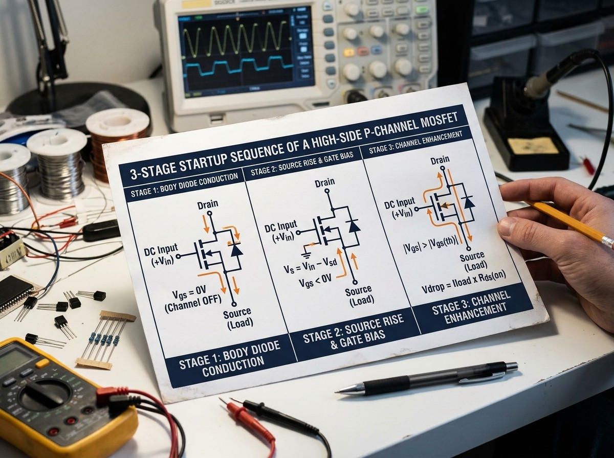
The 3-Stage Startup Sequence (Through the Intrinsic Body Diode)
A common question among circuit designers is how a high-side P-MOSFET turns on at all when its Source is connected to an unpowered load rail (). The answer lies in the physical orientation of the MOSFET's internal parasitic body diode, which executes a three-stage startup sequence whenever positive DC power is applied:
Stage 1 — Initial Power Application and Body-Diode Conduction: At the instant positive DC voltage () is applied to the Drain, the load side (Source) is atand the MOSFET channel is OFF (). Because the Drain is connected to the input and the Source is connected to the load, the intrinsic Drain-to-Source body diode is forward-biased. Initial current flows through this body diode to charge the downstream load rail.
Stage 2 — Source Potential Rise and Gate Biasing: As current flows through the forward-biased body diode, the Source terminal rises to approximately one body-diode drop below the input rail (). Because the Gate is referenced toward system ground () through a pull-down path, the Source is now positive relative to the Gate, establishing a negative gate-to-source voltage ().
Stage 3 — Channel Enhancement and Body-Diode Shunting: Once the magnitude of the gate-to-source voltage exceeds the MOSFET's gate threshold voltage () and reaches full enhancement, the low-resistance PMOS channel turns on in parallel with the intrinsic body diode. Load current immediately diverts from the high-drop body diode into the low-channel, collapsing the voltage drop across the device to.
Hidden Startup Risk — Low-Voltage Brownout and Linear-Region Heating:
If your minimum DC input voltage () is too close to the MOSFET's threshold voltage, the circuit gets trapped between Stage 2 and Stage 3. Instead of driving the MOSFET fully into its low-resistance ohmic enhancement region, an insufficientleaves the transistor operating in its resistive linear region (or conducting partially through the parasitic body diode). Under load current, a partially enhanced MOSFET dissipates substantial heat and can suffer thermal failure during brownout conditions. Always select a P-MOSFET whose datasheet specifies a low, guaranteedat alower than your minimum expected supply voltage.
Why Schematics and AI Answers Disagree: The "Upside-Down" Drain-vs-Source Orientation Trap
One of the most frequent causes of board respins—and a point where even automated AI search summaries and novice schematics directly contradict each other—is the pin orientation of the P-channel MOSFET.
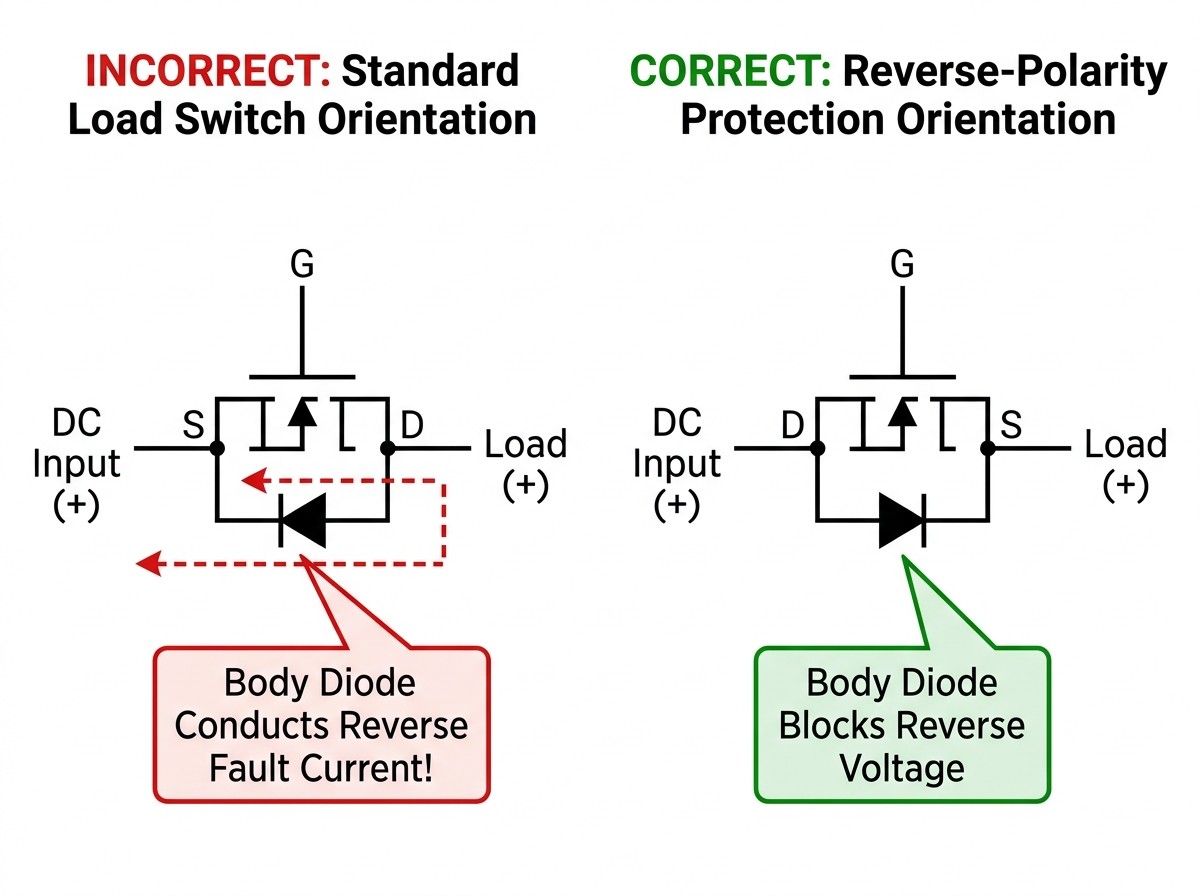
In a conventional high-side load switch, the P-MOSFET is wired with its Source connected to the power supply and its Drain connected to the load so that when the gate is pulled high (switch OFF), the internal body diode is reverse-biased and blocks current from reaching the load. For a deeper look at standard switching configurations, see our guide on how to design reliable high-side switching circuits with P-channel MOSFETs.
However, if you wire a reverse polarity protection circuit like a standard load switch (Source to DC input, Drain to load), the circuit will fail completely during a reverse-polarity fault. As emphasized by Monolithic Power Systems and EEPower, in a P-channel MOSFET, the intrinsic body diode's anode is internally tied to the Drain and its cathode is tied to the Source. If the Source faces the DC input and a battery is connected backward (), the Drain/load side sits at a higher potential () than the negative Source terminal. That forward-biases the body diode, conducting destructive reverse current straight through the MOSFET even though the gate channel is turned off.
To block reverse polarity, you must invert the MOSFET relative to a load switch:
| Circuit Parameter | Standard High-Side Load Switch | High-Side Reverse-Polarity Protection |
|---|---|---|
| MOSFET Drain Connection | Connected to Load (+) | Connected to DC Input (+) |
| MOSFET Source Connection | Connected to DC Input (+) | Connected to Load (+) |
| Intrinsic Body Diode Anode | Faces Load (Drain side) | Faces DC Input (Drain side) |
| Intrinsic Body Diode Cathode | Faces DC Input (Source side) | Faces Load (Source side) |
| Normal Polarity () Behavior | Body diode blocks when switch is OFF; channel conducts when Gate is pulled low | Body diode conducts at startup to raise Source, then channel turns ON and shunts body diode |
| Reverse Polarity () Behavior | Fails to protect: Body diode becomes forward-biased and conducts reverse current | Protects load: Channel stays OFF () and body diode is reverse-biased |
Gate Protection and Absolute Maximum Ratings: Preventing MOSFET Breakdown
Tying a P-channel MOSFET's Gate directly to system ground exposes its gate oxide to the full DC input rail (). Whenever the maximum DC supply voltage or transient surge can exceed the MOSFET's absolute maximumrating, designers must place a Zener clamping diode between Gate and Source alongside a current-limiting resistor to ground—clampingsafely belowwhile still pulling the gate far enough below the source to drive the MOSFET out of its linear region into full enhancement.
Why Direct-to-Ground Gate Wiring Ruptures Gate Oxide
On a low-voltage rail where the peak supply voltage never approaches the transistor's maximum gate-to-source voltage rating (), connecting the P-MOSFET Gate directly to ground is sufficient. However, as highlighted in onsemi AND90146-D, Diodes Incorporated AN1192, and EEPower, power MOSFETs have thin gate oxides whose absolute maximumlimits are typically much lower than their drain-to-source voltage ratings (). On industrialsupplies, wide-range battery packs, or automotiverails subject to load-dump and inductive switching spikes, tying the gate directly to ground imposesacross the gate-source terminals and immediately punctures the gate oxide.
The Zener Diode + Pull-Down Resistor Clamp Network
To protect the gate oxide on higher-voltage inputs, engineers add two passive components: a Zener clamping diode placed directly in parallel across the MOSFET Source and Gate terminals (Zener cathode connected to Source, Zener anode connected to Gate) and a series bias resistor () connecting the Gate node to system ground.
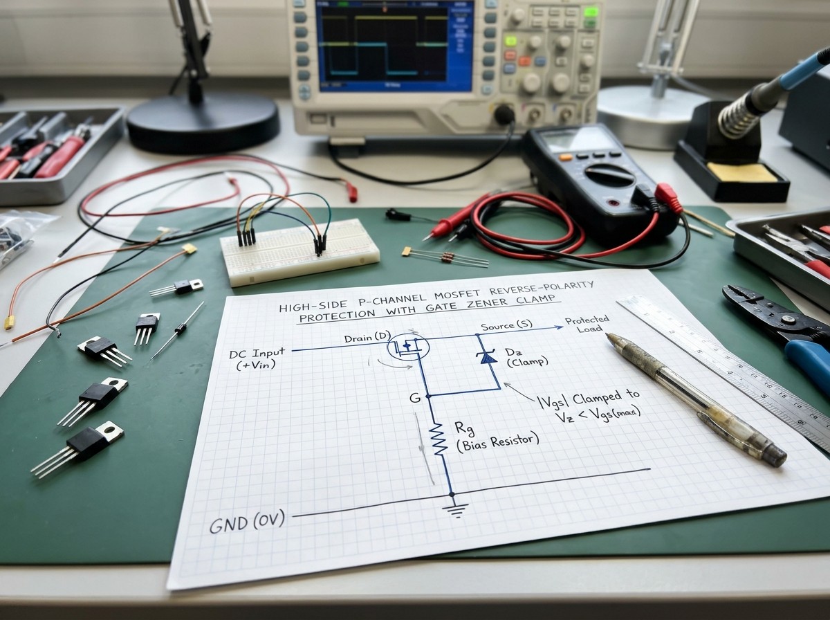
Normal Polarity Clamping (): When the positive input voltage rises above the Zener breakdown voltage (), the Zener diode conducts in reverse breakdown and clamps the gate-to-source voltage to. The series resistordrops the excess rail voltage () to ground and limits Zener current.
Driving the MOSFET Out of the Linear Region: The small bias current flowing from the Source rail, through the Zener/gate network, and down throughto ground is not merely parasitic waste. Designers must sizeand(or use a parallel gate-source resistor withto form a resistive voltage divider on predictable rails) so that across the entire operating voltage range,stays safely belowat high line while remaining large enough at low line to drive the PMOS completely beyond its linear region into full enhancement. If the gate bias is starved,rises sharply and thermal dissipation () can overheat the package.
Reverse Polarity Behavior (): When input leads are swapped andgoes negative, the Zener diode becomes forward-biased from Gate (connected toward ground via) to Source. This clamps the positive gate-to-source voltage near a single forward diode drop (), ensuring the P-MOSFET channel stays firmly OFF whilelimits reverse leakage current from ground into the negative input rail.
CheckingUnder Hot-Swap and Capacitive Hold-Up Stress
A common design oversight is checking the MOSFET's drain-to-source breakdown voltage () only against the nominal DC supply voltage. In real-world applications, the drain-source junction faces far higher stress during dynamic faults:
Capacitive Hold-Up Doubling (): As documented in onsemi
AND90146-D, if a circuit has large bulk reservoir capacitors on the load side charged toand the input terminals are suddenly hot-swapped or switched to(dynamic reverse polarity), the MOSFET Source remains held atwhile the Drain drops to. That imposes a total voltage ofacross the Drain-Source terminals[3].Repetitive Inductive Line Transients: In automotive and industrial systems, negative inductive switching transients superimpose high-voltage spikes onto the input line. For example, in STMicroelectronics' PCIM Europe validation, automotive P-channel protection stages are tested not only against dynamic switching fromto, but also against 5,000 repetitive negative pulses atper ISO 7637-2 Pulse 1.
Rather than relying on arbitrary voltage-multiplier rules of thumb, calculate the worst-casestress by summing your maximum held-up output rail voltage with the peak negative supply or transient clamp voltage specified by your system's surge standard, and verify that it remains within the datasheet's safe operating envelope.
Application Boundaries: Who Should Not Choose Each Option (and When Active Control Is Required)
While a self-biased high-side P-channel MOSFET blocks static reverse battery connections, an enhanced MOSFET channel conducts current bidirectionally and cannot prevent a charged output capacitor or battery from back-feeding a sagging or shorted input rail. Systems requiring dynamic reverse-current blocking, redundant power OR-ing, or high-current efficiency must step up to an active ideal-diode controller driving an N-channel MOSFET.
Who Should NOT Choose a Series Diode
Low-Voltage or Battery-Operated Devices: Any circuit where losing a diode forward drop () triggers premature regulator dropout or wastes a major fraction of battery energy (such as thetodrop demonstrated in TI
SLVA139).Medium-to-High Current Rails: Designs exceeding the typical 2 A to 3 A low-current window where linear diode power loss () creates unacceptable PCB hotspots.
Who Should NOT Choose a Self-Biased High-Side P-MOSFET
Ultra-Low-Voltage Rails: Inputs where the minimum supply voltage approaches, preventing full channel enhancement without an external boost rail.
High-Current Power Rails: Because holes have lower carrier mobility in silicon than electrons, P-channel MOSFETs require a larger die area (and higher cost) to achieve the same lowas an N-channel MOSFET of equivalent voltage rating.
Systems Vulnerable to Dynamic Reverse Current (The Back-Feeding Blind Spot): As detailed by Texas Instruments (
SLVAE57B), Diodes Incorporated (AN1192)[8], and Analog Devices, a self-biased high-side P-MOSFET only turns off when the Source voltage falls near or below the Gate potential. If downstream bulk hold-up capacitors or a connected battery hold the Source pin positive while the input supply suddenly shorts to ground or sags below the output voltage,remains greater than. Because an enhanced MOSFET channel conducts equally well in both directions, current flows backward from the load into the sagging input supply, discharging your hold-up capacitance or draining the battery. When designing battery-interfacing stages that must prevent backflow and reverse hookup simultaneously, review our specialized analysis on reverse voltage protection for battery chargers.
Evaluating the Alternatives: Low-Side N-MOSFET vs. High-Side Ideal-Diode Controllers
When neither a series diode nor a passive high-side P-MOSFET fits the application, engineers evaluate two N-channel MOSFET topologies:
Low-Side N-Channel MOSFET (In the Ground Return Path): Placing an N-channel MOSFET in the negative return line (Drain to load ground, Source to power supply negative terminal, Gate biased from the positive rail via a Zener/resistor clamp) lets you use lower-cost, lower-N-MOSFETs without a charge pump. However, placing a switch in the ground path introduces a voltage offset between system ground and supply ground, and disconnects the ground reference during a fault—creating severe ground-loop and signal-integrity hazards in systems with shielded cables, single-ended communication buses, or shared chassis grounds.
High-Side N-Channel MOSFET + Active Ideal-Diode Controller IC: To keep the protection switch on the positive high-side rail while using an N-channel MOSFET, an active ideal-diode or reverse-polarity controller IC uses an integrated charge pump to drive the N-MOSFET gate above the supply rail (for instance, Analog Devices demonstrates charge-pump protection circuitry operating across battery rails fromtowhile boosting the N-MOSFET gate to[5]). Furthermore, as explained in TI
SLVAE57Band Diodes IncorporatedAN1192, active ideal-diode controllers continuously monitor the millivolt forward drop across Drain and Source, pulling the gate down rapidly to turn the MOSFET off the instant current begins to reverse[2]—isolating output hold-up capacitors from input shorts and micro-interruptions.
A Note on Vendor Application Notes: Many semiconductor application notes are published by IC manufacturers to showcase proprietary ideal-diode controller chips. If your circuit does not require active reverse-current blocking (back-feed isolation) and operates at moderate current where P-MOSFETeasily meets thermal limits, a discrete 3-component P-MOSFET circuit remains simpler and more economical than an active controller IC.
Component Selection, Sourcing, and Bench Verification Checklist
A reliable reverse polarity protection circuit review verifies physical device orientation alongside worst-case electrical stress against datasheet absolute maximum ratings. For P-channel MOSFET stages, engineers must confirm that the Drain faces the DC input so the body diode blocks reverse voltage, verify thatstays belowat peak input voltage, and confirm thatis specified at the minimum available gate drive.
Part A: Circuit Designer's Datasheet and Schematic Verification Checklist
1. Schematic Polarity and Pinout Verification
Series Diode Orientation: Confirm the Anode connects to the DC Input (+) and the Cathode connects to the Load (+).
High-Side P-MOSFET Orientation: Confirm the Drain connects to the DC Input (+) and the Source connects to the Load (+), with the schematic symbol's intrinsic body diode arrow pointing from Drain (input) toward Source (load).
Gate Zener Clamp Orientation: Confirm the Zener Cathode connects to the MOSFET Source and the Zener Anode connects to the MOSFET Gate (so it operates in Zener breakdown during normal polarity and forward-biases during reverse polarity).
2. Absolute Maximum Voltage Rating Checks
Diode Peak Reverse Voltage (): Verify in the datasheet thatexceeds the maximum reverse DC supply voltage plus worst-case inductive line transients (especially critical when selecting low-barrier Schottky diodes).
MOSFET Drain-to-Source Breakdown (): Verify thatexceeds worst-case dynamic reverse voltage (when output hold-up capacitors are charged towhile the input is switched to) plus clamped transient surges per your system standard (such as ISO 7637-2).
MOSFET Gate-to-Source Rating (): Verify that the maximum Zener clamp voltage (at peak bias current and temperature tolerances) stays safely below the MOSFET's absolute maximumlimit.
3. Low-Voltage Startup and Thermal Dissipation Checks
Full Channel Enhancement at Minimum: Verify that at, the gate-to-source voltagedeveloped across the Zener/resistor network exceedsand reaches the datasheet test condition where lowis guaranteed, preventing linear-region overheating.
Junction Temperature () Margin: Calculate steady-state conduction loss (for diodes;at hotfor MOSFETs) plus high-temperature reverse leakage dissipation (for Schottky diodes), and verify against package thermal resistance () for your actual PCB copper pad area (onsemi
AND90146-D).Gate Resistor () Power Rating: Calculate resistor power dissipation during normal high-line operation () and during sustained reverse polarity (), ensuring the resistor package rating includes adequate thermal derating.
Part B: Repair Engineer's Bench Diagnostic Protocol
When troubleshooting a dead DC power input stage on the repair bench, work through these four diagnostic checks before reapplying power:
Test Shunt Crowbar Diodes When a Fuse Is Blown: If an input fuse is open, inspect any parallel TVS or crowbar diode across the post-fuse rail. A prolonged reverse-polarity connection frequently causes a shunt TVS diode to fail as a dead short—or thermally fracture open if the diode burned out before a slow-blow fuse cleared.
Test the Gate-Source Zener Before Replacing a Burned P-MOSFET: If a high-side P-MOSFET has overheated or blistered, measure the Gate-to-Source Zener diode out of circuit. If an overvoltage spike shorted the Zener diode (), soldering in a new P-MOSFET without replacing the shorted Zener will prevent the new FET's channel from turning on—forcing full load current through its parasitic body diode and burning up the replacement MOSFET under load.
Verify PCB Footprint Pinout Against the Datasheet: Never assume a blown SOT-23, SO-8, or DPAK transistor on a DC input is wired like a standard load switch. Trace the PCB continuity from the input connector positive pin to confirm it lands on the MOSFET Drain pad.
Perform a Millivolt Drop Test Under Load: After repairing a P-MOSFET protection stage, apply normal DC voltage under nominal load current and measure the DC voltage drop directly from Drain to Source (). A properly enhanced MOSFET will drop only millivolts (). If you measure hundreds of millivolts across the FET, the channel is either off (conducting solely through the body diode) or stuck in the linear region due to insufficient gate bias.
Part C: Component Sourcing, Authenticity, and Lifecycle Considerations
Counterfeit and Remarked MOSFET Hazards: In field repairs and contract manufacturing, counterfeit power MOSFETs often contain smaller silicon dies or remarked lower-grade parts with much higherand weaker gate oxide breakdown margins than the authentic datasheet specifies. On an input protection rail, remarked silicon quickly overheats at rated load current or suffers gate rupture during normal line transients. Always procure power MOSFETs and protection diodes through traceable, authorized supply chains.
Qualification Grade Verification: For automotive, heavy vehicle, or industrial control boards exposed to repetitive reverse-battery or cold-crank transients, verify that candidate P-MOSFETs and diodes carry appropriate qualification (such as AEC-Q101 for automotive discrete semiconductors, as validated in STMicroelectronics and onsemi application literature) and confirm active production status before finalizing your PCB footprint.
Frequently Asked Questions (FAQ)
Does a diode in series protect against reverse polarity?
Yes. Wiring a rectifier or Schottky diode in series with the positive DC supply line blocks current when the power leads are connected backward, because the diode becomes reverse-biased (Texas Instruments SLVA139, Analog Devices). However, because load current flows through the junction continuously during normal operation, it causes a permanent forward voltage drop () and linear heat loss (), limiting it mainly to low-current circuits.
How do you wire a P-channel MOSFET for reverse polarity protection?
Connect the P-channel MOSFET on the positive high-side rail with its Drain connected to the DC power input and its Source connected to the load—the exact opposite of a standard high-side load switch (Monolithic Power Systems, EEPower). This orientation ensures the internal body diode conducts briefly at startup to establish gate bias under normal polarity, but becomes reverse-biased to block current when polarity is inverted.
Why does a P-channel MOSFET reverse polarity circuit need a Zener diode?
Tying a P-MOSFET gate directly to ground exposes its thin gate oxide to the full DC input rail voltage. Whenever the maximum input voltage or line transients can exceed the MOSFET's absolute maximum gate-to-source rating (), placing a Zener diode across Gate-Source with a pull-down resistor to ground clampswithin safe limits while still driving the channel into full enhancement (onsemi AND90146-D, EEPower).
Which type of MOSFET is best for reverse polarity protection: P-channel or N-channel?
A high-side P-channel MOSFET is simpler for low-to-medium currents because it requires only a passive resistor and Zener clamp referenced to ground. An N-channel MOSFET provides lowerand smaller die size for high-current rails, but must either sit in the ground return path (disrupting system ground integrity) or use a high-side charge-pump ideal-diode controller IC (onsemi AND90146-D, TI SLVAE57B, Diodes Incorporated AN1192).
Sources and references used for this guide
Reverse Current/Battery Protection Circuits
Source type: official company documentation
Used for: Supports series diode reverse-battery protection principles and reverse-bias blocking behavior.
Caution: Official vendor application report; use for circuit topology mechanics rather than unextracted numeric tables.Application Note - Basics of Ideal Diodes
Source type: official company documentation
Used for: Supports the application boundary between simple reverse-polarity protection and active ideal-diode controllers.
Caution: Official vendor application note; do not treat controller IC examples as neutral product rankings.AND90146 - MOSFET Selection for Reverse Polarity Protection
Source type: official company documentation
Used for: Supports comparing diodes, P-channel MOSFETs, and N-channel MOSFETs for DC input and automotive ECU reverse-polarity protection.
Caution: Official semiconductor documentation; do not attribute unverified AI derating multipliers (such as 1.5x VDS) to this note.Designing a Reverse Polarity Protection Circuit (Part I)
Source type: vendor article
Used for: Supports the typical 2A to 3A low-current application range for series diodes and explains how the P-channel MOSFET parasitic body diode blocks reverse polarity.
Caution: Single vendor educational source for the 2A-3A guideline; frame the current range as a typical rule of thumb dependent on thermal limits.Reverse-Current Circuitry Protection
Source type: official company documentation
Used for: Supports framing mechanical vs. electrical reverse-battery safeguards and placing a series diode in the positive supply rail.
Caution: Official vendor design note; use for foundational circuit principles.Reverse Battery Protection Scheme for Automotive Applications
Source type: official company documentation
Used for: Supports the trade-off of achieving low insertion loss at low cost in reverse-battery protection schemes.
Caution: Official vendor technical document; keep topology comparisons vendor-neutral.Automotive-grade P-channel Power MOSFETs for Static, Dynamic Reverse Polarity Protection
Source type: official company documentation
Used for: Supports the use of P-channel power MOSFETs to protect electronic control units during reverse-polarity events.
Caution: Manufacturer conference paper; use for P-MOSFET protection topology validation.Understanding the Different Approaches to Input Reverse Voltage Protection (AN1192)
Source type: ai cited source
Used for: Supports comparing self-biased P-channel MOSFET circuits with N-channel MOSFETs driven by ideal-diode controllers.
Caution: AI-cited official semiconductor application note; use for high-level topology comparison.
 UTMEL

We are the professional distributor of electronic components, providing a large variety of products to save you a lot of time, effort, and cost with our efficient self-customized service. careful order preparation fast delivery service
 Reverse-Polarity Protection for DC Inputs: Diode and MOSFET Trade-OffsUTMEL24 October 202617
This technical guide compares series diodes and high-side P-channel MOSFETs for DC input reverse-polarity protection. It analyzes forward voltage drop, conduction power loss, and the three-stage startup sequence through the MOSFET body diode. Designers and repair engineers also gain practical verification checklists covering drain-to-source orientation, Zener gate clamping, absolute maximum voltage ratings, and when to step up to active ideal-diode controllers.
Read More All You Need to Know About Rectifier CircuitUTMEL24 April 202518186
All You Need to Know About Rectifier Circuit
Read More 15 Key Elements of Diode SelectionUTMEL26 November 202119491
Hello everyone, I am Rose. Welcome back to the new post today. Diodes are one of the most common components in our circuit boards. So, what factors should be considered when selecting models?
Read More What is a PIN Diode?UTMEL04 February 202110628
While diodes with a simple PN junction are by far the most common type of diode in operation, in a variety of applications, other forms of diode may be used. The PIN diode is one type that is used for a number of circuits. In a variety of places, this diode type is used. For RF switching, the PIN diode is very fine, and the PIN structure in photodiodes is very useful as well.
Read More Microwave Diode: Introduction and TypesUTMEL07 January 202126608
Microwave diodes are diodes that work in the microwave frequency band. It is a solid-state microwave device. Microwave band usually refers to the frequency from 300 MHz to 3000 GHz. After the discovery of the point contact diode effect at the end of the 19th century, microwave diodes such as PIN diodes, varactor diodes, and Schottky diode tubes appeared one after another. Microwave diodes have the advantages of small size and high reliability, and are used in microwave oscillation, amplification, frequency conversion, switching, phase shifting and modulation.
Read More
Subscribe to Utmel !
![742792031]() 742792031
Würth Elektronik
![MMZ1608S301ATA00]() MMZ1608S301ATA00
TDK Corporation
![FBMJ4516HS720NT]() FBMJ4516HS720NT
Taiyo Yuden
![BLM18AG221SH1D]() BLM18AG221SH1D
Murata Electronics
![MMZ2012S102AT000]() MMZ2012S102AT000
TDK Corporation
![HZ0603B112R-10]() HZ0603B112R-10
Laird-Signal Integrity Products
![BLM18EG601SH1D]() BLM18EG601SH1D
Murata Electronics
![BLM18AG151SN1D]() BLM18AG151SN1D
Murata Electronics
![MMZ1005S102CT000]() MMZ1005S102CT000
TDK Corporation
![BLM18HD471SN1D]() BLM18HD471SN1D
Murata Electronics


