Basic Guidelines for Mixed-Signal PCB Layout Design
To reduce, if not completely eliminate, signal interference, mixed-signal PCB design requires a fundamental grasp of analog and digital circuits. In order to maintain the signal integrity of the entire system, the components of a modern system must function in both the digital and analog domains.
PCB layout is a challenging step in the mixed-signal development process, and component placement is just the beginning. The layers of the board and how to effectively manage those layers must also be taken into account in order to reduce interference brought on by parasitic capacitances that can unintentionally form between layers between PCB planes.
A crucial component of the PCB layout design for mixed-signal systems is grounding. Even though the subject of grounding is frequently discussed in the business, engineers may find it challenging to come up with a consistent method. An difficulty with high-quality grounding, for instance, can have an impact on the layout of the entire high-performance mixed-signal PCB design. As a result, this factor should not be disregarded.
Ⅰ. Component placement
Before installing circuit components, a floor design for the system must be made, much like when building a house. This procedure should assist prevent high noise signal interference and establish the overall integrity of the system architecture.
It is advised, particularly for high-speed circuits, to follow the signal path shown on the schematic when creating a floor design. Another crucial component of the design is where the components are placed.
To decide where to put the system's components, designers should be able to recognize crucial functional blocks, signals, and linkages between blocks. For instance, it is desirable to locate connectors on the board's edge, while it is necessary to position auxiliary parts like decoupling capacitors and crystals as close as possible to mixed-signal devices.
Ⅱ. Separation of analog and digital modules
To minimize the common return path for analog and digital signals, consider analog and digital block separation so that analog signals do not mix with digital signals.

Figure 1. Analog and Digital Circuit Separation
Figure 1 shows a good example of the separation of analog and digital circuits. The following When dividing the analog and digital portions, it should be kept in mind:
It is advised to install delicate analog components in the analog plane, such as amplifiers and references. The opposite side/digital plane must be used for noisy digital components like logic control and timing blocks.
An analog-to-digital converter (ADC) or digital-to-analog converter (DAC) in the system that is mixed-signal and has a low digital current can be handled in a manner similar to how analog components are handled in the analog plane.
It is advised to separate the analog and digital power supply for designs with numerous high-current ADCs and DACs. In other words, DVDD should be connected to the digital part and AVCC must be attached to the analog part.
The space and heat produced by microprocessors and microcontrollers can be significant. For improved heat dissipation, these components must be positioned in the board's center and have to be near the circuit blocks that they are meant to be connected to.
Ⅲ. Power module
The power supply is a crucial component of the circuit and needs to be treated with care. Power modules must, as a general rule, be proximate to the components they power while being isolated from the rest of the circuit.
Dedicated power modules can be utilized for the analog and digital sections when devices in complicated systems have many power pins in order to prevent noisy digital interference.
To reduce inductance and prevent current limitation, power lines should be short, straight, and use wide traces.
Ⅳ. Decoupling technology
One of the crucial factors that designers must take into account in order to meet the system's desired performance is the Power Supply Rejection Ratio (PSRR). The performance of the device is ultimately determined by PSRR, which assesses the gadget's sensitivity to changes in the power supply.
Preventing high frequency energy from entering the device is required to maintain ideal PSRR. Using a mix of electrolytic and ceramic capacitors, the device power supply can be effectively isolated from a high impedance ground plane for this purpose.
A low noise environment is what effective decoupling is meant to achieve for circuit operation. The fundamental rule is to provide the shortest path possible to make it simple for the current to return.
Designers must pay close attention to each device's high frequency filtering suggestions. More importantly, this checklist will act as a manual for generic decoupling methods and how to use them correctly:
Low inductance ceramic capacitors are used to reduce high frequency noise, while electrolytic capacitors are utilized to lessen low frequency noise on the power supply by acting as charge reservoirs for transient currents. Additionally, ferrite beads are optional but enhance isolation and decoupling from high frequency noise.
Decoupling capacitors need to be positioned as close as possible to the device's power supply pins. To reduce extra series inductance, these capacitors should be linked to greater portions of the low impedance ground plane using vias or short wires.
The device's power supply pins should be as close to the device as possible. Smaller capacitors (usually 0.01F to 0.1F) should be used. This configuration avoids the device from operating in an unstable manner when several outputs are switching at once. The distance between electrolytic capacitors and the device's power pins should not exceed one inch (10F to 100F on average).
The decoupling capacitors can be T-connected to the ground plane using vias close to the device's GND pin to simplify construction instead of constructing traces. See Figure 2 for a demonstration.
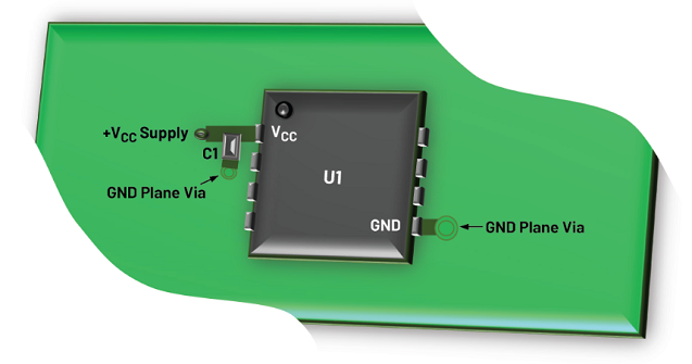
Figure 2. Decoupling Techniques for Power Pins
Ⅴ. Circuit board layer
We can examine a different part of the board design, also known as the board layer, once the component arrangement and floor plan are finished. Before PCB routing, it is highly advised to take into account the board layers, since these will influence the permissible return paths for the system design.
The vertical arrangement of copper layers of a circuit board is referred to as the "circuit board layers." These layers are responsible for controlling the board's current and signals.
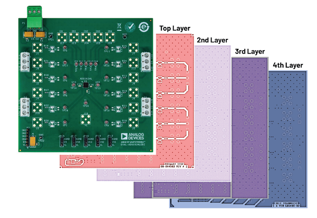
Figure 3. Example of a 4-layer PCB
Figure 3 shows a visual representation of the layers of the board. Figure. 4 details the setup of a typical 4-layer PCB:

Figure 4. Typical 4-layer PCB
A high-performance data collection system should typically contain four layers or more. Auxiliary signals are often used in the bottom layer whereas digital/analog signals are typically used in the top layer. By serving as a reference plane for impedance control signals, the second layer (also known as the ground plane) lowers IR drop and protects digital signals in the top layer. On the third layer, the power plane is located.
Due to the additional inter-plane capacitance they provide, the power and ground planes must be close to one another for the power supply to be decoupled at high frequencies.
The suggestions for mixed-signal designs for ground planes have evolved throughout time. For many years, it made sense to divide the ground plane into analog and digital, but a new strategy is now being put forth for contemporary mixed-signal devices. Problems caused by high levels of noise in the signals should be avoided with proper floor planning and signal separation.
Ⅵ. Ground planes: to separate or not to separate?
In the design of a mixed-signal PCB layout, grounding is a crucial step. To guarantee that the return signal returns along a low impedance channel, a standard 4-layer PCB must contain at least one layer devoted to the ground plane. To reduce series inductance and resistance, all IC ground pins should be placed on a low impedance ground plane and linked directly to it.
Separating analog and digital grounds has become a common grounding technique for mixed-signal systems. However, a single ground works best for managing mixed-signal devices with modest digital currents. Additionally, designers must take needs for mixed-signal current into account when deciding which grounding technique is best. Designers must take into account two grounding techniques.
Ⅶ. Single ground plane
The optimal strategy would be to use a single solid ground plane for mixed-signal systems with a single low digital current ADC or DAC. It is necessary to analyze return currents in order to comprehend the significance of a single ground plane. The term "return current" describes the flow of current that completes a circuit loop and flows back to ground. Each return path must be followed throughout the PCB layout to avoid mixed-signal interference.
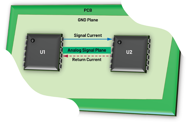
Figure 5. Return Current for a System Using a Solid Ground Plane
Figure 4's straightforward circuit illustrates the benefits of a single solid ground plane over many ground planes. An equal but opposing return current exists to the signal current. The path of least resistance is taken by this return current as it returns to its source in the ground plane.
The route of least resistance, which is often a straight line between the device ground references, will be followed by the return current for low frequency transmissions. However, a portion of the return current will attempt to travel back along the signal channel for higher frequency transmissions. This is due to the lower impedance and smaller loop generated between the outgoing and returning currents along this channel.
Ⅷ. Separate analog ground and digital ground
Separate grounding may be preferable in complex systems where a strong grounding method is challenging. Another typical strategy is to divide the ground plane into two halves, the analog ground plane and the digital ground plane. This is appropriate for more complicated systems with numerous mixed-signal components and high digital current requirements. An illustration of a system with a divided ground plane is shown in Figure 5.

Figure 6. Return Current for a System Using a Split Ground Plane
Eliminating ground plane breaks and allowing return currents to take a more direct path, flowing back through the star ground junction, is the simplest way to accomplish integral grounding for systems having separate ground planes. In mixed-signal layout ideas, the intersection of the analog and digital ground planes is known as a star ground.
A star ground can be connected to a typical thin continuous connection between the analog and digital ground planes in common systems. Star grounding is typically performed for more intricate systems by shunting a jumper wire to the ground connection.
Because a star ground has no current flow, high-current-carrying headers and jumper shunts are not necessary. A star ground's primary function is to guarantee that the reference level for both grounds is the same.
To ensure compliance with grounding standards and to prevent grounding-related problems, designers should carefully read the grounding suggestions offered in each device's data sheet.
On the other hand, because the star ground also connects both grounds at one place, mixed-signal devices with AGND and DGND pins can be connected to their respective ground planes. This separates delicate analog circuitry from high-noise digital currents, which travel through the digital power supply, all the way to the digital ground plane, and back to the digital power supply. The multilayer PCB must accomplish complete isolation of the AGND and DGND planes.
Ⅸ. Other Common Grounding Practices
To guarantee that appropriate grounding strategies are applied in mixed-signal/digital systems, the following procedures or checklist might be used:
Wide copper traces should be used to connect to the star's ground point.
Look out for any narrow traces on the ground plane; these connections should be avoided.
It is advantageous to have pads and vias so that, if necessary, analog and digital ground planes can be connected.
Ⅹ. In conclusion
Making a component floorplan is just the first step in PCB planning for mixed-signal applications, which can be difficult. One of the crucial factors a system designer must take into account when attempting to achieve the best performance in a mixed-signal system layout is properly controlling board layers and creating a suitable grounding scheme.
The overall integrity of the system design will be established with the use of a component floor plan, and the management of currents and signals across the board will be facilitated by properly arranging the board layers. Last but not least, selecting the best grounding strategy will enhance system performance and stop issues brought on by high noise signals and return currents.
 HF PCB Circuit Design 10 QuestionsUTMEL16 March 20224993
Hello everyone, I am Rose. Today I want to give you a full explanation about PCB design. I Hope the following ten questions will give you a satisfied answer.
Read More How Many do You Know About the 12 Components Included in the Circuit Board?UTMEL12 February 20228142
We are lucky to live in an era where electronic devices are readily available. These electronic devices, on the other hand, come to us thanks to the incredible components on the circuit board, and we frequently wonder what makes electronic devices operate, how they achieve such massive success, and how they accomplish it. Electronic devices are incredible things; you can't see what's going on within them, but you can see what they're capable of. We'll talk about the wonders of PCBs and how to get past them to construct the circuit board in this article.
Read More![50 Frequently Asked Questions about PCB Layout [Q&A] 50 Frequently Asked Questions about PCB Layout [Q&A]](https://res.utmel.com/Images/Article/b5ce2a0a-d37c-4243-aff3-df7b2da2db0f.jpg) 50 Frequently Asked Questions about PCB Layout [Q&A]UTMEL16 November 20216759
50 Frequently Asked Questions about PCB Layout [Q&A]UTMEL16 November 20216759In the design of electronic products, PCB layout and routing is an important step, and the quality of PCB layout and routing will directly affect the performance of the circuit.
Read More An Overview of Development BoardUTMEL18 December 202514574
The development board is a circuit board used for embedded system development. Development boards are generally customized by embedded system developers according to development needs.
Read More PCB Design GuidelinesUTMEL21 December 20217011
Hello everyone, I am Rose. Today I will provide you a comprehensive guideline of PCB design.
Read More
Subscribe to Utmel !
![PRQ200W-Q48-S36-H-D]() PRQ200W-Q48-S36-H-D
PRQ200W-Q48-S36-H-DCUI Inc.
![PRQ200W-Q48-S15-D]() PRQ200W-Q48-S15-D
PRQ200W-Q48-S15-DCUI Inc.
![AQM200PS19]() AQM200PS19
AQM200PS19XP Power
![AQM250PS24]() AQM250PS24
AQM250PS24XP Power
![AM1LR-1215SH30JZ]() AM1LR-1215SH30JZ
AM1LR-1215SH30JZaimtec
![AM1SR-2405SJZ]() AM1SR-2405SJZ
AM1SR-2405SJZaimtec
![AM1LS-0524SH30JZTR]() AM1LS-0524SH30JZTR
AM1LS-0524SH30JZTRaimtec
![AM10T-1205SNZ]() AM10T-1205SNZ
AM10T-1205SNZaimtec
![AM1LS-2412SH30JZTR]() AM1LS-2412SH30JZTR
AM1LS-2412SH30JZTRaimtec
![AM1DS-1515SJZ]() AM1DS-1515SJZ
AM1DS-1515SJZaimtec


 Product
 Brand
Brand Articles
 Tools
Tools


